Built-in electric field and strain tunable valley-related multiple topological phase transitions in VSiXN4 (X= C, Si, Ge, Sn, Pb) monolayers
Abstract
The valley-related multiple topological phase transitions attracted significant attention due to their providing significant opportunities for fundamental research and practical applications. However, unfortunately, to date there is no real material that can realize valley-related multiple topological phase transitions. Here, through first-principles calculations and model analysis, we investigate the structural, magnetic, electronic, and topological properties of VSiXN4 (X = C, Si, Ge, Sn, Pb) monolayers. VSiXN4 monolayers are stable and intrinsically ferrovalley materials. Intriguingly, we found that the built-in electric field and strain can induce valley-related multiple topological phase transitions in the materials from valley semiconductor to valley-half-semimetal, to valley quantum anomalous Hall insulator, to valley-half-semimetal, and to valley semiconductor (or to valley-metal). The nature of topological phase transition is the built-in electric field and strain induce band inversion between the dxy/dx2-y2 and dz2 orbitals at K and valleys. Our findings not only reveal the mechanism of multiple topological phase transitions, but also provides an ideal platform for the multi-field manipulating the spin, valley, and topological physics. It will open new perspectives for spintronic, valleytronic, and topological nanoelectronic applications based on these materials.
I Introduction
Valley degree of freedom and related manipulations have become rising topics in recent years 1 ; 2 . It is coupled with the spin degree of freedom to exhibit extraordinary quantum effects Li1 ; 3 ; 4 ; 5 ; Li2 , such as the valley spin Hall effect 6 ; 7 , and valley polarized quantum anomalous Hall effect (VQAHE) 3 ; 4 ; 8 ; 9 ; 10 . The coupling effects are typically strong in the transition metal elements with localized d electrons, and the effects will be further enhanced with the decrease of dimensions. Therefore, two-dimensional (2D) transition metal materials provide a good opportunity to investigate the manifestation of quantum covariation effects of charge, spin, topological, and valley.
In the 2D hexagonal lattice material, the extreme value of the valence and conduction bands are appeared at the K and points, forming the valley degrees of freedom. Due to the effect of the inversion symmetry () breaking together with spin-orbit coupling (SOC), the K and valleys have opposite spins but degenerate energies, which is called as spin-valley locking. As a result, the charged carriers in the two opposite valleys were selectively stimulated by the photons with left-hand and right-hand circular polarization. In addition, if the system further breaks time-reversal symmetry (), the valley degenerate will disappear at K and points. It is named as ferrovalley 11 . Therefore, exploring ferrovalley materials is beneficial to promoting the development of spintronics and valleytronics.
Recently, a new 2D transition metal material MoSi2N4 family has been successfully synthesized in the experiment 12 , and more than 60 stable ternary compounds with similar structures have been predicted theoretically 13 . Such a family of materials has many interesting physical properties, including intrinsic magnetism, valley polarization, transport, and topology 14 ; 15 ; 16 ; 17 ; 18 . It was noticed that the 2D Janus transition metal dichalcogenides (TMDs) were also experimentally synthesized 19 . It is well known that the MoSi2N4 family is the combination of TMDs and SiN surface layers. Thence, Janus MoSi2N4 family is also very hopeful to be prepared. The two chalcogen layers are different, and the mirror symmetry in the Janus MoSi2N4 family is broken. The impact of spontaneous out-of-plane dipole (the built-in electric field) and strain on the covariation effect (charge, spin, topological, and valley) may be crucial, but has not been clearly understood yet.
In this work, we systematically investigate the built-in electric field and strain on the covariation effect of spin, topological, and valley freedom of the VSiXN4 (X= C, Si, Ge, Sn, Pb) monolayers. It is found that the built-in electric field and strain effects can induce a series of topological phase transitions, such as valley semiconductor (VSC), valley-half-semimetal (VHSM), valley quantum anomalous Hall insulator (VQAHI) and valley-metal (VM). It essentially originated from the built-in electric field and strain-induced band inversion between the dxy/dx2-y2 and dz2 orbitals at K and valleys. Our findings create pathways for valley-related multiple topological phase transitions and further microelectronic devices with the perfect valley, spin, and topology.
II STRUCTURES AND COMPUTATIONAL METHODS
To explore the electronic and magnetic structures, we used the Vienna Simulation Package (VASP) 20 ; 21 ; 22 within the framework of the density functional theory (DFT) for the first-principles calculations. The exchange-correlation energy was described by the generalized gradient approximation (GGA) with the Perdew-Burke-Ernzerhof (PBE) functional 23 . The plane-wave basis with a kinetic energy cutoff of 500 eV was employed, and and -centered meshes were adopted for structural optimization and self-consistent calculations. A vacuum of 20 was set along the c-axis, to avoid the interaction between the sheet and its periodic images. The total energy convergence criterion and the force were set to be 10-7 eV and -0.001 eV/, respectively. To describe strongly correlated 3d electrons of V 11 ; 24 , the GGA+U method is applied. The Coulomb repulsion U is varied between 1 eV and 4 eV. To confirm the results, the calculations are also checked with Heyd-Scuseria-Ernzerhof (HSE06) method. To investigate the dynamical stability, the phonon spectra were calculated using a finite displacement approach as implemented in the PHONOPY code 25 . The maximally localized Wannier functions (MLWFs) were employed to construct an effective tight-binding Hamiltonian to explore the Berry curvature, anomalous Hall conductivity (AHC), and edge states 26 . The calculated the AHC, it performed the Berry curvature calculations using the formula
| (1) |
| (2) |
| (3) |
where C is Chern number, is the Berry curvature in the reciprocal space, and are operator components along the x and y directions, and for the occupied bands, respectively 39 ; 40 ; 41 . One can obtain the Chern number as well as AHC by integrating the Berry curvature in the entire Brillouin zone (BZ). Therefore, the edge states were calculated in a half-infinite boundary condition using the iterative Green’s function method by the package WANNIERTOOLS 27 .
III RESULTS AND DISCUSSION
III.1 Structure and stability
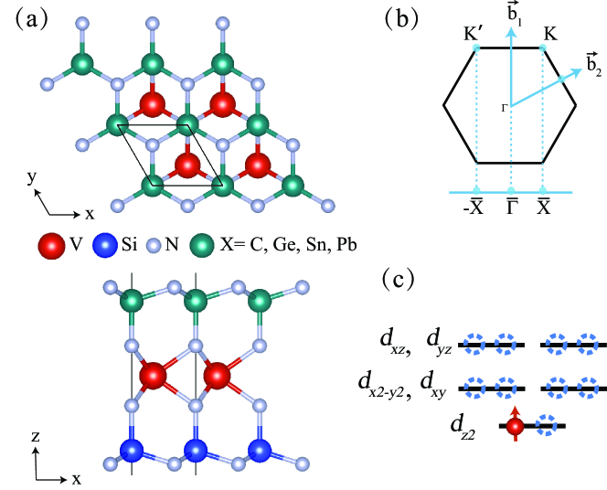
The crystal structure of the VSiXN4 monolayer is shown in Fig. 1(a). VSiXN4 consists of septuple layers of N-Si-N-V-N-X-N, with atoms in each layer forming a 2D hexagonal lattice. Each V atom is coordinated with six N atoms, forming a trigonal prismatic configuration, and then this VN2 layer is sandwiched by Si-N and X-N layers. The space group of VSiXN4 is P3m1 (No. 156), and the space inversion symmetry is broken [except VSi2N4, it is P-6m2 (No. 187)]. The lattice constant of VSi2N4 is optimized to 2.88 , agreeing well with previous work 12 ; 14 . However, the lattice constant of VSiCN4, VSiGeN4, VSiSnN4, and VSiPbN4 are optimized to 2.75 , 2.95 , 3.04 and 3.07 (See Table I), respectively. The lattice constant is increasing with the increase of the X atomic order. To confirm the stability of VSiXN4 monolayers, the phonon spectra are calculated. As shown in Fig. S1, the absence of imaginary frequencies confirms that the VSiXN4 monolayers are dynamically stable. Only VSiPbN4 has a small imaginary frequency at the point, it is the numerical error. In previous reports Ge ; LuoWei , it is a common problem for 2D materials. These imaginary frequencies become smaller as we increase the supercell in the phonon spectrum calculations. In addition, as shown in Fig. S2, we calculated the formation energy for 2H and 1T phase VSiXN4. The formation energy is expressed as Ef = (Etot - - - 4)/N, where Etot is the total energy of the VSiXN4. The , , and are the chemical potential V, X, and N atoms, respectively. N is the number of atoms in VSiXN4. As listed in Table SI, the negative value, -6.390 eV 7.504 eV, indicates that the VSiXN4 lattice is a strongly bonded network and hence favors its experimental synthesis. Even though 1T phase formation energy of VSiGeN4, VSiSnN4, and VSiPbN4 is lower than that of the 2H phase formation, the difference is very small. In addition, to confirm the dynamical stability of the 1T phase VSiXN4, we calculated the phonon spectrum, as shown in Fig. S3. We found that the phonon spectrum of 1T phase VSiXN4 has a large imaginary frequency. It indicates that the dynamics of 1T phase VSiXN4 are unstable.
| a | MAE | - | - | Eg | |
|---|---|---|---|---|---|
| VSiCN4 | 2.75 | 96.66 | 46.73 | 0.00 | 722.04 |
| VSi2N4 | 2.88 | 50.98 | 63.74 | 0.00 | 381.33 |
| VSiGeN4 | 2.95 | -4.16 | 70.17 | 0.00 | 0.00 |
| VSiSnN4 | 3.04 | -17.41 | 0.00 | 68.86 | 118.91 |
| VSiPbN4 | 3.07 | -30.27 | 0.00 | 72.45 | 0.00 |
III.2 Magnetic property
The valence electron configuration of the V atom is 3d34s2. After donating four electrons to the neighboring N atoms, one valence electron is retained. According to Hund’s rule and the Pauli exclusion principle, the electron configuration of V4+ split into three groups: (dz2 orbital), (dxy, dx2-y2 orbital), and (dz2 orbital), as shown in Fig. 1(c). Therefore, the magnetic moment of the VSiXN4 monolayer is expected to be 1 per cell. Our spin-polarized calculations indeed show that VSiCN4, VSi2N4, VSiGeN4, and VSiSnN4 are spin polarized, and that the magnetic moments are mainly distributed over the V atoms, with a magnetic moment of 1 per unit. It is worth noting that only VSiPbN4 the magnetic moment is not 1 (1.09 ). Due to the increase of the out-of-plane dipole formed by Si and Pb atoms, VSiPbN4 becomes a VM.
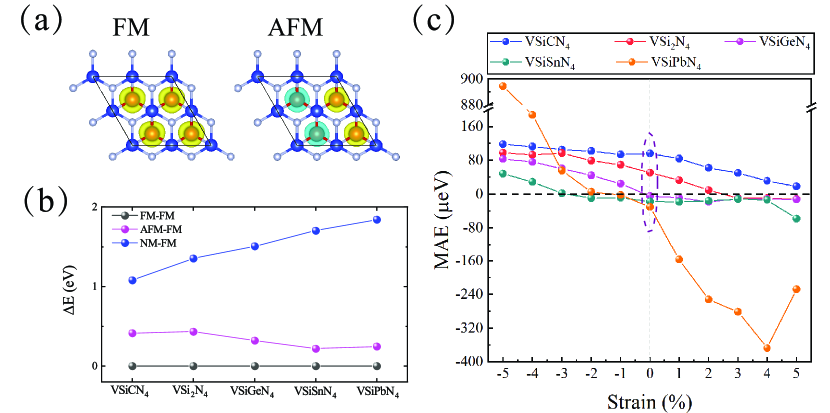
To determine the magnetic ground state of the VSiXN4 monolayer, three possible magnetic configurations are considered, namely, the ferromagnetic (FM), antiferromagnetic (AFM), and non-magnetic (NM) structures [see Fig. 2(a)]. We calculate the total energy difference between the FM, AFM, and NM using the GGA+U method. To determine a reasonable value of U, the GGA+U calculated energy difference between the AFM and FM states compares the HSE06 results, as shown in Fig. S4. It can be found that the value of U near 3 eV is consistent with the results of HSE06 for the VSiXN4 monolayer. Therefore, we choose Ueff = 3 eV to investigate VSiXN4 (X= C, Si, Ge, Sn, Pb) system. By comparing the total energy of FM, AFM, and NM states, we found that the FM configuration is the magnetic ground state for the VSiXN4 monolayer, as shown in Fig. 2(b). The FM ground state of the VSiXN4 monolayer can be understood by studying the crystal structure. In VSiCN4, VSiGeN4, VSiSnN4, and VSiPbN4, the V-N-V bond angles are 87.9∘, 91.4∘, 92.8∘ and 93.1∘, respectively, which are close to 90.0∘. According to the Goodenough-Kanamori-Anderson rule 28 ; 29 ; 30 , this configuration is beneficial to FM coupling.
Then, we investigate the underlying physics for the robust out-of-plane magnetization. The direction of spin-polarization orientation is determined by magnetic anisotropy energy (MAE), which is defined as MAE = Ez - Ex/y. Firstly, we tested the convergence of K-mesh before calculating MAE. As shown in Fig. S5, when the K-mesh is , the convergence criterion is reached completely. The MAE is calculated using K-mesh in Fig. 2(c). The MAE value is listed in Table I. For magnetic ions V with a finite orbital moment, MAE can estimate through the formula , where , L, and S represent the strength of SOC, orbital angular momentum, and spin angular momentum 31 , respectively. For the VSiXN4 monolayer, the half-filled and empty e1, e2 orbitals indicate that L = 0 and S = 1/2. Due to the quenched orbital moment, the MAE originating from the SOC of V atom vanishes. Thence, MAE is mainly contributed by the SOC effect originating from N and X (X = C, Si, Ge, Sn, Pb) atoms. The MAE can be written as 32 ; 33 ; 34
| (4) |
where o and u denote to the occupied and unoccupied states, respectively. The spin indices and run over 1, amounting to each of the two orthogonal spin states at the K point. Eu,σ, and E are the band energy of the states. As shown in Fig. S6, u and o are mainly contributed by N px and py orbitals. The contribution from the X (X = C, Si, Ge, Sn, Pb) atomic orbitals is almost negligible. Therefore, u and o can be written as aτ = ax + iay from V atoms and p = px + ipy from N atoms, where = 1 and = 1. Thence, MAE can be simplified as
| (5) |
where is the band gap, and L = and L = i,
| (6) |
The spin orientation is determined by the orbital overlaps of and . In a purely octahedral crystal environment, the irreducible representations of the p and pz of the ligands are EEg and AA2u, respectively. aτ of V atoms belongs to Eg, which indicates that aτ trends to couple with p instead of pz from N atoms. Thus, . It indicates that the MAE favors a positive value, benefiting the out-of-plane spin orientation. In fact, VSiCN4 and VSi2N4 have an easy magnetization plane, while the easy axes of VSiGeN4, VSiSnN4, and VSiPbN4 are along the out-of-plane direction, as shown in Fig. 2(c). It is attributed to the MAE tunable by the strong dipole interaction of the system. MAE is an intrinsic property of the material. There are many factors affecting the MAE of materials, such as spin-orbit coupling, structure, orbital occupation and so on. In VSiXN4, MAE is mainly determined by the built-in electric field. As shown in Fig. 4(b), in the absence of strain, the VSiCN4 has the largest built-in electric field. Besides, the built-in electric field is 0.36 V/ (VSiCN4), 0.16 V/ (VSiGeN4), 0.26 V/ (VSiSnN4), and 0.31 V/ (VSiPbN4), respectively. Exactly, the MAE is 96.66 eV (VSiCN4), -4.16 eV (VSiGeN4), -17.41 eV (VSiSnN4), and -30.27 eV (VSiPbN4), respectively. The variation law of MAE is completely consistent with that of the built-in electric field. In addition, as shown in Fig. 2(c), we found that the tensile strain favors an out-of-plane magnetism. It is originated from that the tensile strains reduce the distance between Si and X atoms, thus enhancing dipole interactions.
III.3 Electronic band structure
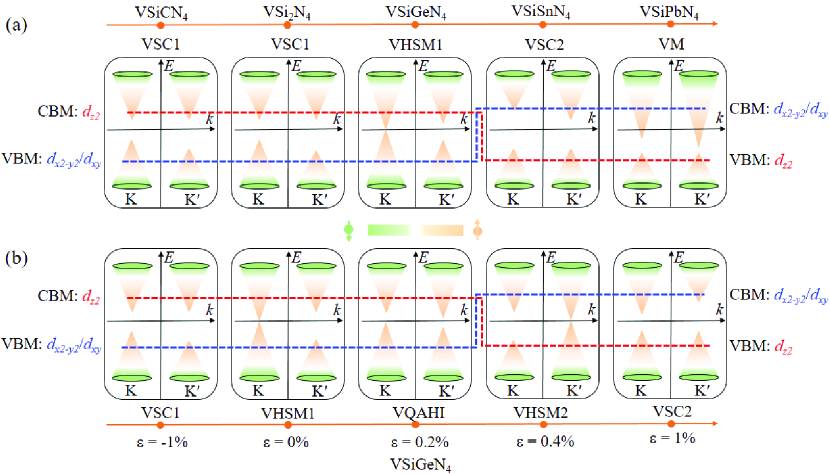
In addition, we first calculated the band structure of VSiXN4 with spin polarization but without SOC. As shown in Fig. 3(a), it can be found that there is a valley at each of the K and points. Both the valence and conduction bands of the valleys are spin up bands. The two valleys are degenerate in energy. More interestingly, as the atomic number of X increases, it exhibits abundant electronic structure properties. VSiCN4, VSi2N4, and VSiSnN4 are VSC, while VSiGeN4 and VSiPbN4 are VHSM and VM, respectively. So we further calculated the band structures with the SOC effect. As shown in Fig. 3(b, c), it can be found that the valence band valley of K is appreciably higher than for the VSiCN4, VSi2N4, and VSiGeN4, while the conduction band valley of K is obviously lower than K′ for VSiSnN4. Therefore, the valley degeneracy is broken and an evident valley splitting - or - is induced. - (or - ) is 46.73 meV, 63.74 meV, 70.17 meV, 68.86 meV and 72.45 meV for VSiCN4, VSi2N4, VSiGeN4, VSiSnN4, and VSnPbN4 (See Table I), respectively.
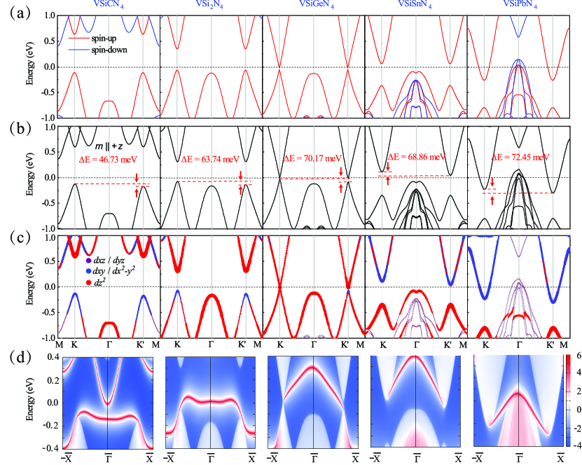
Here, it exhibits a novel phenomenon. The valley polarization of VSiCN4, VSi2N4, and VSiGeN4 only appears at the valence band, while it degenerates at the conduction band. Be the opposite, the valley splitting of VSiSnN4 and VSiPbN4 occurs at the conduction band. It is important that VSiGeN4 is the critical state, and valence band maximum (VBM) and conduction band minimum (CBM) appear degeneracy at the K point forming a Dirac cone. From the orbital resolved band structure, as shown in Fig. 3(c), the VBM bands of VSiCN4, VSi2N4, and VSiGeN4 are mainly contributed by V dxy/dx2-y2 orbitals, while the CBM bands are dominated by dz2 orbitals of V atom. For VSiSnN4 and VSiPbN4 monolayer, on the contrary, the VBM bands are primarily dz2 orbital, while the CBM are mainly dxy/dx2-y2 orbitals. It can be found that the atomic number of the X atom induced band inversion between the dxy/dx2-y2 and dz2 orbitals. As is well known, the orbital angular momentum of dz2 orbital is zero. Thence, dz2 orbital doesn’t occur valley splitting. Notably, these results yield a good comparison with the band structures obtained from the HSE06 method, as shown in Fig. S7.
To understand the underlying mechanism for the ferrovalley effect in VSiXN2. Here, we take VSiGeN4 as an example to perform model analysis. We adopted vτ=(dxy+idx2-y2), cτ=(dz2) as the orbital basis for the VBM and CBM, where = 1 indicate the valley index corresponding to . Since the VBM and CBM belong to the same spin channel (spin up bands), we take the SOC effect as the perturbation term, which is
| (7) |
where and are spin angular and orbital angular operators, respectively. and represent the interaction between the same spin states and between opposite spin states, respectively. For the VSiGeN4 monolayer, the single valley is composed of only one spin channel [see Fig. 3(a)], and the other spin channel is far from the valleys. Hence, the term can be ignored. On the other hand, can be written in polar angles
| (8) |
In the out-of-plane magnetization case, = = 0, then the term can be simplified as
| (9) |
The energy levels of the valleys for the VBM and CBM can be expressed as Evτ = vτ vτ and Ecτ = cτ cτ , respectively. Then, the valley polarization in the valence and conduction bands can be expressed as
| (10) |
| (11) |
where the = -2i, = 2i. The analytical result certificates that the valley degeneracy splits for the valence and conduction bands are consistent with our DFT calculations ( - = 70.17 meV, - = 0.00 meV).
III.4 Built-in electric field induced topological phase transition
To reveal the topological properties of VSiXN4 monolayers, we have calculated the local density of states of the edge state through the Green’s function method 35 . As shown in Fig. 3(d), only the VSiGeN4 monolayer exists a single topologically protected edge state appeared in between the conduction and valence bands. It indicates that only VSiGeN4 could be topologically non-trivial, while the others are topologically trivial.
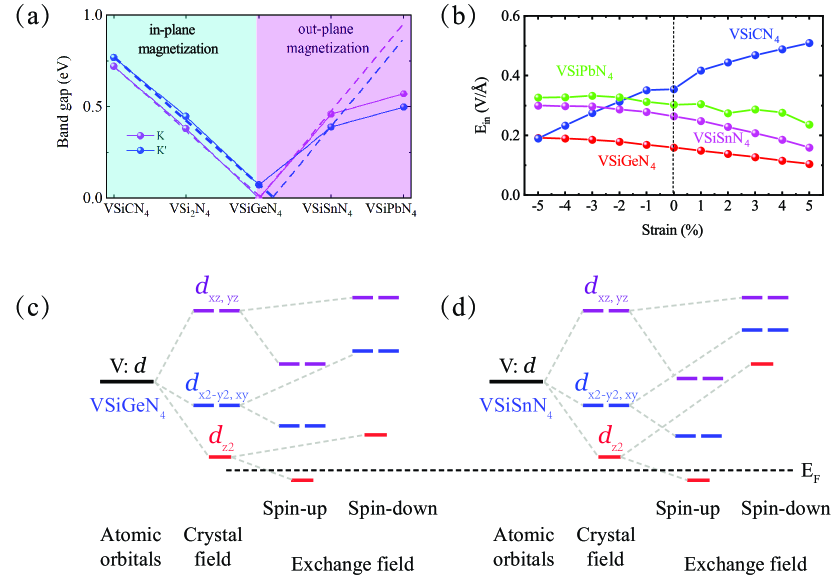
It is noticed that an interesting topological phase transition from VSC to VHSM, to VSC, and to VM appears with the atomic number of X element increasing for the magnetic VSiXN4 monolayers [see Fig. 3(b)] For instance, the topological phase transition occurs in VSiGeN4 (VHSM). Through the detailed analysis on the energy band variation with the atomic number of the X element, it is found that the topological properties are closely related to the gap at the K and points. As shown in Fig. 4(a), as the atomic number of X increases, the gap at the K and points gradually decreases to zero in VSiGeN4. The fitting curve shows that the band gap at the K and points would reach zero when X is Ge, which is the phase transition point. We further analyzed the built-in electric field. The built-in electric field is caused by the asymmetric Janus structure. Therefore, as shown in Fig. S8, the built-in electric field is defined as Ein = ( - )/, where and represent the electrostatic potential at the bottom and top of VSiXN4, respectively. The is the structural height of VSiXN4. As shown in Fig. 4(b), more surprisingly, the variation trend of the built-in electric field is completely consistent with the variation trend of the band gap of K and . The built-in electric field is 0.36 V/ (VSiCN4), 0.00 V/ (VSi2N4), 0.16 V/ (VSiGeN4), 0.26 V/ (VSiSnN4), and 0.31 V/ (VSiPbN4), respectively. It means that the built-in electric field induces a topological phase transition. To prove this, we analyzed the energy level assignments of V-d orbitals for VSiGeN4 and VSiSnN4, as shown in Fig. 4(c, d). Seeing is believing. It is a band inversion between dxy/dx2-y2 and dz2 orbitals at the K and points in VSiSnN4. Note that the built-in electric field introduced by the element, which does not change continuously. VSiGeN4 is the critical point, therefore, only VSiGeN4 is topologically non-trivial. The continuous variation of the built-in electric field will be described in detail below. In addition, it is well known that applied electric fields can tune the band gap, magnetic ground state, topological properties, and so on. In previous reports Liu ; Qian , the electric field is an effective method to tune topological phase transition. The intrinsic built-in electric field tunes topological phase transition that is rarely reported.
III.5 Strain induced topological phase transition
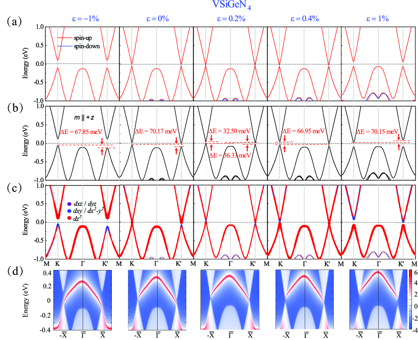
For a 2D material, its electronic structure can be generally tuned effectively by strain 36 ; 37 ; 38 . In the following, we investigate the effect of biaxial strain on the spin, valley, and topological properties of VSiXN4. Here, we focus on one representative VSiGeN4. In the calculations, the biaxial strain is defined as = (a-a0)/a0100. In the formula, a and a0 represent lattice constant after and before in-plane biaxial strain is applied, respectively. As shown in Fig. 5(a-c), by increasing strain within a reasonable range (-5 5), when , the material enters into a VSC. While = 0 , the band gap at K point is firstly closed, meanwhile the band gap decreases to 70.17 meV at point. Hence, the VHSM states are acquired in the material. When employ the tensile strain, the band gap at K point reopens. At the other critical case with = 0.4 , the band gap of point recloses, and the valleys at become a Dirac cone-shaped linear dispersion. Continuing applying the tensile strain to 0.4 , the band gap at the point reopens, and it again becomes a VSC.
To understand the mechanism of multiple topological phase transitions, we analyze the orbital projected band structures and berry curvature. As shown in Fig. 5(c) and Fig. S9, the compressive strain is 1, the VBM is dominated by the dxy and dx2-y2 orbitals of V atoms, while the CBM mainly comes from the dz2 orbital. The Berry curvatures at K and have opposite signs. More interestingly, the tensile strain is used (0.2 tensile strain is shown in Fig. 5), and the band gap of the K point reopens. The band inversion occurs between dxy/dx2-y2 and dz2 orbitals at the K point, while the orbital order doesn’t change at the point. Surprisingly, the Berry curvature of K and become of the same sign. It is a characteristic of VQAHI. It is also confirmed by the calculation of edge states [See Fig. 5(d)]. After the band gap at is closed ( = 0.4 ). Continuing applying the tensile strain, there is also a band inversion between dxy/dx2-y2 and dz2 orbitals at the point. The signs of the Berry curvatures around the flip. Thus, the system returns to the VSC again.
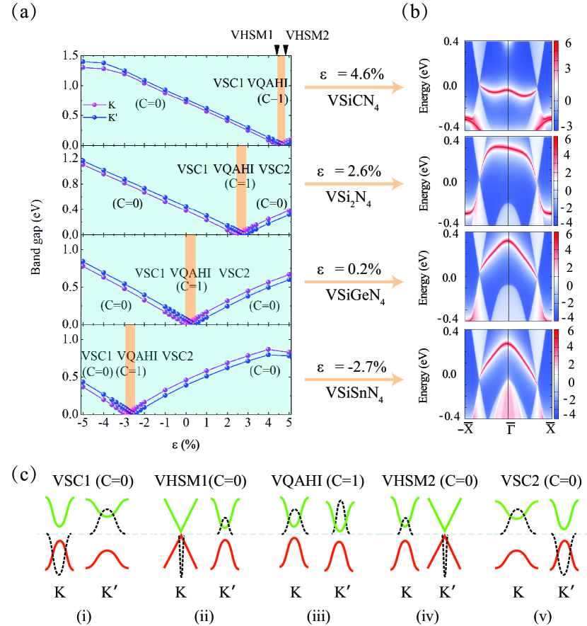
To further demonstrate the universality of strain-induced band inversion mechanism in the VSiXN4 system, we systematically investigated the topological properties of VSiXN4 under different strains (band structure shown in Fig. S10-S14). As shown in Fig. 6(a,b), it is found that the strain can induce band inversions, which lead to the topological phase transition in these systems. Note that the range of the VQAHI states is different in VSiCN4 (4.5 4.8), VSi2N4 (2.5 2.9), VSiGeN (0.0 0.4), and VSiSnN4 (-2.9 -2.5). To facilitate the reader’s understanding, we also give a table, as listed in Table SII. Most important of all, the valley-related multiple topological phase transitions originate from the change of the sign of the Berry curvatures at K and points. How the band gaps and the topological phase vary with the various strain for the VSiXN4 monolayers are summarized in Fig. 6(c). It is found that the strain magnitude required to achieve topological phase transition is highly dependent on the built-in electric field. We also found that the strain can effectively tune the built-in electric field, then, it induces the band inversion to realize topological phase transition. In addition, we calculated the results for different U values, as shown in Fig. S15. When the Ueff is 1 eV and 2 eV, the VSiXN4 system doesn’t have topological properties, while the Ueff increase to 3 eV and 4 eV, the VSiXN4 system will appear topological phase with the built-in electric field and strain. Therefore, the band structures vary with the built-in electric field, and strain for VSiXN4 monolayers is summarized in Fig. 7.
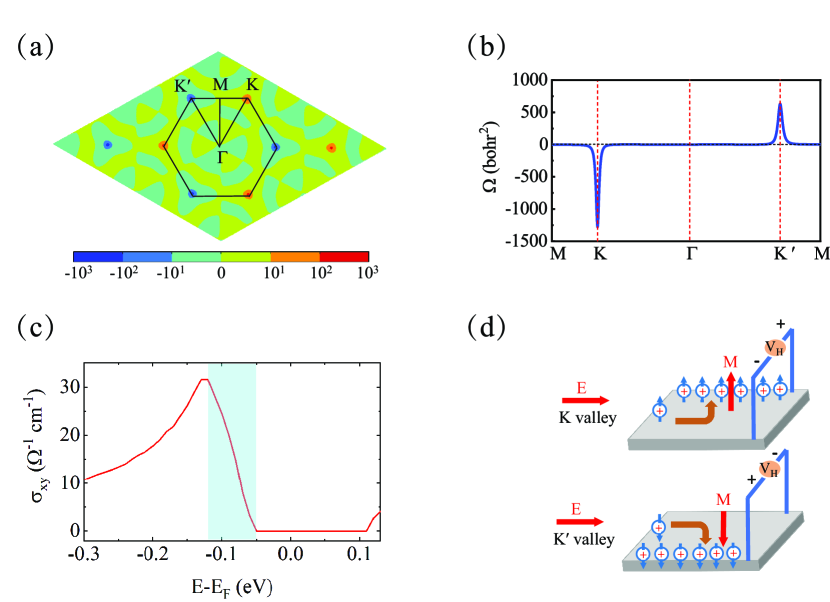
To characterize the valley-contrasting physics in VSiXN4 monolayer. We take the VSiGeN4 of -1 strain as an example. The Berry curvature of -1 strain VSiGeN4 in the entire 2D BZ and along the high symmetry line are shown in Fig. 8(a, b). Clearly, the Berry curvatures at K and points have opposite signs, showing the typical valley polarization characteristic. By integrating the Berry curvature over the BZ, one can further calculate the AHC. As shown in Fig. 8(c), a valley-polarized Hall conductivity clearly exists in the -1 strain VSiGeN4 monolayer. Specifically, when the Fermi level lies between the VBM or CBM of the K and valleys, as denoted by the cyan region, a fully spin- and valley-polarized Hall conductivity is generated. This result confirms the existence of valley anomalous Hall effect in the -1 strain VSiGeN4 monolayer. Moreover, in the hole-doping condition, when the magnetism direction of VSiGeN4 is in the +z direction, the spin up holes from the valley will be generated and accumulate on one boundary of the sample under an in-plane electrical field [upper plane of Fig. 8(d)]. On the other hand, when the magnetism direction is in the -z direction, the spin-up holes from the K valley will be generated and accumulate on the opposite boundary of the sample under an in-plane electrical field [lower plane of Fig. 8(d)]. This feature shows that monolayer VSiGeN4 is an ideal candidate for the high-performance valleytronic devices.
IV CONCLUSION
In conclusion, we have demonstrated the rich multi-field induced physics in VSiXN4 (X = C, Si, Ge, Sn, Pn) monolayers. The rich topological phase transitions can be realized through the built-in electric field and strain. Taking the VSiGeN4 monolayer as an instance, when 0 and 0.4, it is a valley semiconductor. Moreover, the quantum anomalous Hall insulator is obtained with tensile 0.0 0.4. At the two critical cases with = 0.0 and 0.4, the valleys at K and become a Dirac cone, respectively. It becomes a valley-half-semimetal. We reveal that the nature of topological phase transition is built-in electric field and strain induces band inversion between the dxy/dx2-y2 and dz2 orbitals at K and valleys. The abundant topological phase transition makes the VSiXN4 monolayers a very promising material to develop intriguing spin-valley-topology devices.
ACKNOWLEDGEMENTS
This work is supported by the National Natural Science Foundation of China (Grant No. 12004295). P. Li thanks China’s Postdoctoral Science Foundation funded project (Grant No. 2022M722547), and the Open Project of State Key Laboratory of Surface Physics (No. KF202209). This work was calculated at Supercomputer Center in Suzhou University of Science and Technology.
References
- (1) D. Xiao, W. Yao, and Q. Niu, Phys. Rev. Lett. 99, 236809 (2007).
- (2) J. R. Schaibley, H. Yu, G. Clark, P. Rivera, J. S. Ross, K. L. Seyler, W. Yao, and X. Xu, Nat. Rev. Mater. 1, 1 (2016).
- (3) P. Li, X. Li, W. Zhao, H. Chen, M. X. Chen, Z. X. Guo, J. Feng, X. G. Gong, and A. H. MacDonld, Nano Lett. 17, 6195 (6195).
- (4) S. Li, Q. Wang, C. Zhang, P. Guo, and S. A. Yang, Phys. Rev. B 104, 085149 (2021).
- (5) K. Wang, Y. Li, H. Mei, P. Li, and Z. X. Guo, Phys. Rev. Mater. 6, 044202 (2022).
- (6) K. Sheng, Q. Chen, H. K. Yuan, and Z. Y. Wang, Phys. Rev. B 105, 075304 (2022).
- (7) P. Li, X. S. Zhou, and Z. X. Guo, NPJ Comput. Mater. 8, 20 (2022).
- (8) K. F. Mak, K. He, J. Shan, and T. F. Heinz, Nat. Nanotechnol. 7, 494 (2012).
- (9) A. Srivastava, M. Sidler, A. V. Allain, D. S. Lembke, A. Kis, and A. Imamoglu, Nat. Phys. 11, 141 (2015).
- (10) J. Zhou, Q. Sun, and P. Jena, Phys. Rev. Lett. 119, 046403 (2017).
- (11) X. Feng, X. Xu, Z. He, R. Peng, Y. Dai, B. Huang, and Y. Ma, Phys. Rev. B 104, 075421 (2021).
- (12) X. Zhou, R. W. Zhang, Z. Zhang, W. Feng, Y. Mokrousov, and Y. Yao, NPJ Comput. Mater. 7, 160 (2021).
- (13) W. Y. Tong, S. J. Gong, X.Wan, and C. G. Duan, Nat. Commun. 7, 13612 (2016).
- (14) Y. L. Hong, Z. Liu, L. Wang, T. Zhou, W. Ma, C. Xu, S. Feng, L. Chen, M. L. Chen, D. M. Sun et al., Science 369, 670 (2020).
- (15) L. Wang, Y. Shi, M. Liu, A. Zhang, Y.-L. Hong, R. Li, Q. Gao, M. Chen, W. Ren, H. M. Cheng et al., Nat. Commun. 12, 2361 (2021).
- (16) Q. R. Cui, Y. M. Zhu, J. H. Liang, P. Cui, and H. X. Yang, Phys. Rev. B 103, 085421 (2021).
- (17) C. Yang, Z. Song, X. Sun, and J. Lu, Phys. Rev. B 103, 035308 (2021).
- (18) J. Huang, P. Li, X. Ren, and Z. X. Guo, Phys. Rev. Applied 16, 044022 (2021).
- (19) H. Zhong, W. Xiong, P. Lv, J. Yu, and S. Yuan, Phys. Rev. B 103, 085124 (2021).
- (20) Y. T. Ren, L. Hu, Y. T. Chen, Y. J. Hu, J. L. Wang, P. L. Gong, H. Zhang, L. Huang, and X. Q. Shi, Phys. Rev. Mater. 6, 064006 (2022).
- (21) A. Y. Lu, H. Zhu, J. Xiao, C. P. Chuu, Y. Han, M. H. Chiu, C. C. Cheng, C. W. Yang, K. H. Wei, Y. Yang, et al. Nat. Nanotechnol. 12, 744 (2017).
- (22) G. Kresse and J. Hafner, Phys. Rev. B 47, 558 (1993).
- (23) G. Kresse and J. Furthmuller, Phys. Rev. B 54, 11169 (1996).
- (24) G. Kresse and D. Joubert, Phys. Rev. B 59, 1758 (1999).
- (25) J. P. Perdew, K. Burke, and M. Ernzerhof, Phys. Rev. Lett. 77, 3865 (1996).
- (26) H. L. Zhuang and R. G. Hennig, Phys. Rev. B 93, 054429 (2016).
- (27) A. Togo, F. Oba, and I. Tanaka, Phys. Rev. B 78, 134106 (2008).
- (28) N. Marzari and D. Vanderbilt, Phys. Rev. B 56, 12847 (1997).
- (29) Y. Yao, L. Kleinman, A. H. MacDonald, J. Sinova, T. Jungwirth, D. S. Wang, E. Wang, and Q. Niu, Phys. Rev. Lett. 92, 037204 (2004).
- (30) X. Wang, J. Yates, I. Souza, and D. Vanderbilt, Phys. Rev. B, 74, 195118 (2006).
- (31) D. J. Thouless, M. Kohmoto, M. P. Nightingale, and M. den Nijs, Phys. Rev. Lett. 49, 405 (1982).
- (32) Q. S. Wu, S. N. Zhang, H. F. Song, M. Troyer, and A. A. Suluyanov, Comput. Phys. Commun. 224, 405 (2018).
- (33) B. Goodenough, Phys. Rev. 100, 564 (1955).
- (34) J. Kanamori, J. Phys. Chem. Solids 10, 87 (1959).
- (35) P. W. Anderson, Phys. Rev. 115, 2 (1959).
- (36) J. L. Lado, and J. F. Rossier, 2D Mater. 4, 035002 (2017).
- (37) D. Wang, and R. Wu, Phys. Rev. B 47, 14932 (1993).
- (38) S. Cahangirov, M. Topsakal, E. Akturk, H. Sahin, and S. Ciraci, Phys. Rev. Lett. 102, 236804 (2009).
- (39) W. Luo, and H. Xiang, Angew. Chem. Int. Ed. 55, 8575 (2016).
- (40) J. Hu, and R. Wu, Phys. Rev. Lett. 110, 097202 (2013).
- (41) J. Kim, K. W. Kim, B. Kim, C. J. Kang, D. Shin, S. L. Lee, B. C. Min, and N. Park, Nano. Lett. 110, 097202 (2013).
- (42) M. P. Lopez Sancho, J. M. Lopez Sancho, J. M. Lopez Sancho, and J. Rubio, J. Phys. F 15, 851 (1985).
- (43) Q. Liu, X. Zhang, L. B. Abdalla, A. Fazzio, and A. Zunger, Nano Lett. 15, 1222 (2015).
- (44) X. Li, F. Liu, and Q. Wang, Phys. Rev. B 102, 195420 (2020).
- (45) P. Li, and T. Y. Cai, Phys. Chem. Chem. Phys. 22, 549 (2020).
- (46) P. Li, and T. Y. Cai, J. Phys. Chem. C 124, 12705 (2020).
- (47) P. Li, Y. Ma, Y. Zhang, and Z. X. Guo, ACS Appl. Electron. Mater. 3, 1826 (2021).