How to wire a 1000-qubit trapped ion quantum computer
Abstract
One of the most formidable challenges of scaling up quantum computers is that of control signal delivery. Today’s small-scale quantum computers typically connect each qubit to one or more separate external signal sources. This approach is not scalable due to the I/O limitations of the qubit chip, necessitating the integration of control electronics. However, it is no small feat to shrink control electronics into a small package that is compatible with qubit chip fabrication and operation constraints without sacrificing performance. This so-called “wiring challenge” is likely to impact the development of more powerful quantum computers even in the near term. In this paper, we address the wiring challenge of trapped-ion quantum computers. We describe a control architecture called WISE (Wiring using Integrated Switching Electronics), which significantly reduces the I/O requirements of ion trap quantum computing chips without compromising performance. Our method relies on judiciously integrating simple switching electronics into the ion trap chip – in a way that is compatible with its fabrication and operation constraints – while complex electronics remain external. To demonstrate its power, we describe how the WISE architecture can be used to operate a fully connected 1000-qubit trapped ion quantum computer using signal sources at a speed of quantum gate layers per second.
I Introduction
Trapped-ion qubits are one of the most promising approaches to quantum computing, especially in the NISQ era [1, 2]. One of their main superpowers is ion transport, i.e. the ability to physically move ions in space [3]. This enables two powerful features:
-
1.
Qubit reconfiguration. Ion transport allows for flexible qubit routing – that is, changing which qubit is coupled to which other qubits – without relying on error-prone multi-qubit gates [4]. This allows for effective all-to-all connectivity even in a system composed of many uncoupled qubit registers.
-
2.
Transport-assisted gates. Ion transport allows for local control of quantum operation Rabi frequency even when the qubit drive operates at a fixed amplitude. This method can be employed with both laser and microwave qubit drives – as long as they’re spatially inhomogeneous – and has been used for example in [5, 6, 7, 8].
Qubit reconfiguration is the basis of the QCCD architecture [9, 10], which is one of the most promising approaches to trapped-ion quantum computing. The effective all-to-all connectivity – when combined with excellent coherence times [11, 12, 13] – is one of the reasons why trapped-ion systems achieve such high quantum volumes compared to other platforms [14]. On the other hand, quantum gates in today’s QCCD systems are typically implemented by delivering localized externally modulated qubit drives (e.g. laser beams) to individual trap regions. Ion transport is only leveraged in a limited way, e.g. to move an ion away from a laser beam to switch off the interaction. However, as systems grow and off-chip local drive modulation becomes impractical, transport-assisted gates become a powerful tool, as they allow for local control with only a small number of global qubit drives. In other words, transport-assisted gates reduce the problem of implementing quantum gates at scale to the problem of ion transport at scale.
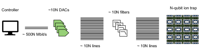
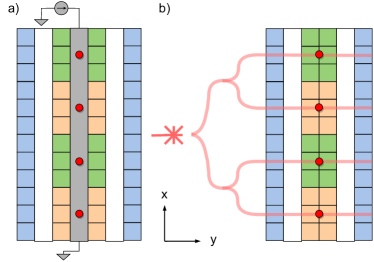
However, the ability to execute ion transport in large-scale systems is hindered by the wiring challenge. Fast, low-heating ion transport requires precise dynamical control of voltages on many electrodes [15, 16]. For example, QCCD architecture demonstrations from Pino et al. [17] and Kaushal et al. [18] both used about 10 electrodes per qubit111For the sake of generality, we will use the term “qubit transport” rather than ion transport. This accommodates for a possibility of encoding one qubit in a short ion chain, or that qubit ions may be always transported in tandem with ancilla ions [19]., each wired to a separate DAC outside of the vacuum system, see Fig. 1. This “standard approach” is likely not scalable even to moderate system sizes. For example, a 1000-qubit chip would require approximately 10,000 input lines – more than today’s cutting-edge CPUs, and at a bleeding edge of packaging feasibility. And while electrode co-wiring has been proposed [20, 21] and used [22, 23] to reduce the number of inputs per electrode, existing co-wiring approaches only allow for limited functionality, such as qubit storage of shuttling between remote zones.
One previously proposed solution to the wiring challenge is to form an integrated “quantum processing unit” (QPU), which combines an ion trap chip with the DACs. The integration could be either monolithic [24] or achieved by packaging together several independently fabricated chips [25]. However, DAC integration comes with major challenges:
-
1.
Power dissipation. For example, Stuart et al. [24] developed compact cryogenic (4K) DACs with a power consumption of mW per channel, or W for 1000 qubits. While this can be optimized, DAC power dissipation presents a significant challenge, especially in cryogenic environments, which are beneficial for reducing noise in trapped-ion systems.
-
2.
Data bandwidth. Fully flexible DAC control requires streaming large volumes of data to the QPU, typically Mbit/s per DAC [18, 26]. For a 1000-qubit QPU, this corresponds to Gbit/s of data flow between the DAC and the control system. Designing an appropriate interface would not be trivial, and in practice might require integration of further digital electronics, for example, to store the waveforms [27]. This increases the complexity of QPU design and fabrication, and may limit the operation flexibility.
-
3.
Footprint. An integrated DAC will typically require a much larger chip area than the electrode itself. For example, a single unfiltered DAC block in [24] used an area of , and lower-noise DAC will require yet larger footprints, especially to accommodate integrated filters. Developing low-noise voltage sources with areas comparable to ion trap electrodes ( or less) is thus a challenge in itself, and might require advanced techniques such as wafer stacking and trench capacitors [28, 29, 30].
Because of the problems highlighted above, current approaches are insufficient to address the wiring challenge, even for intermediate-scale QPUs with qubits.
In this paper, we present an architecture called WISE (Wiring using Integrated Switching Electronics), which addresses the challenge of wiring such intermediate-scale trapped-ion quantum computers. Our method relies on simple integrated electronics that entail minimal power dissipation, low data bandwidth, and small footprint, alleviating all the major challenges of DAC integration. In WISE, all complex high-footprint high-power electronics are placed off-chip, allowing for large-scale control without compromising performance.
The paper is structured as follows. In Sec. II, we give an overview of the electrode wiring architecture and ion transport methods. We then describe how WISE can perform all the key operations of a large-scale QCCD architecture: arbitrary qubit reconfiguration (Sec. III) and transport-assisted gates (Sec. IV). Subsequently in Sec. V we discuss the hardware implementation in more detail, demonstrating that WISE is indeed compatible with ion trap fabrication and operation constraints. Finally, we put it all together in Sec. VI, where we describe how to build a 1000-qubit trapped-ion quantum computer, capable of running arbitrary quantum circuits with all-to-all connectivity but using only input lines.
II WISE method
In a QCCD device, ion positions are controlled by voltages applied to trap electrodes. These electrodes serve two different purposes. The first is dynamic: to deliver time-varying waveforms which execute the desired transport primitives, such as shuttling [31, 32], merging, splitting [33, 34], or crystal rotations [35]. The second is quasi-static: to compensate stray electric fields, generated for example by local charges and differences in work functions [36, 37]. In WISE, each electrode is explicitly assigned to be either dynamic or quasi-static [38, 39]. We then employ two techniques:
-
1.
Dynamic electrode parallelization. Dynamic electrodes are co-wired to a fixed number of DACs, assigned through integrated switches.
-
2.
Quasi-static electrode demultiplexing. Quasi-static “shim” electrodes are controlled through a small number of DACs through integrated demultiplexers in a “sample and hold” fashion.
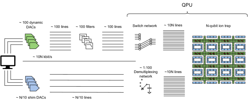
In WISE, instead of DAC integration, we primarily use switch integration. Unlike DACs, switches require very small data input rates and can be operated with negligible power dissipation. Furthermore, they are relatively simple structures, made of a small number of transistors and inverters. Thus, they can be readily integrated into an ion-trap fabrication process [24], and have been demonstrated to be cryogenically compatible, also in the context of quantum computing [40, 41]. The resulting high-level wiring architecture is shown in Fig. 2.
II.1 Dynamic electrode parallelization
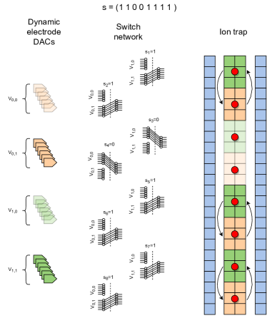
The main observation behind dynamic electrode parallelization is that the same transport operation can be executed in multiple areas of the chip at the same time by applying the same voltage waveforms to multiple electrodes. For example, parallel splits can be executed by connecting one set of DACs, delivering one set of split waveforms, to all the zones where we want to implement a split. Thus, instead of using one DAC per electrode, it suffices to use one DAC per waveform. Furthermore – as we argue in Sec. III.5 – while it might be optimal to execute different transport operations in different zones at the same time (for example, a split in some zones, and a merge in some other zones), it is nonetheless efficient to only perform only one transport operation at any given time (for example, a split in some zones, followed by a merge in some other zones). Thanks to these two ideas, a modest number of DACs suffices to execute arbitrary transport sequences.
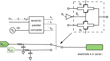
Fig. 2 (top) illustrates the dynamic electrode wiring that leverages those insights. Outside the QPU, a fixed number of DACs are used to output qubit transport waveforms, while in the QPU, switches are used to select which electrode connects to which DAC. In subsequent sections, we show how dynamic electrode parallelization allows for efficient qubit reconfiguration in 1D and 2D ion traps (Sec. III), and why DACs suffice for the purpose, regardless of qubit number . In Sec. IV.1 we discuss how dynamic electrode parallelization can be used to perform transport-assisted quantum gates. Finally, Sec. V.1 describes the hardware implementation of the dynamic electrode switch network.
II.2 Quasi-static electrode demultiplexing
In WISE, all electrodes which are not dynamic are quasi-static, meaning they are held at a constant voltage during any given qubit reconfiguration and during any given quantum gate 222We say “quasi” to indicate that the voltage can be adjusted between steps, for example, a different voltage set can be used for transport and for gates.. The main insight is that holding a fixed voltage on electrodes can be less resource-intensive than applying time-dependent waveforms, because electrodes can maintain their set voltage even while disconnected from DACs. Thus, a single DAC can be demultiplexed to control multiple electrodes. In this mode of operation, the DAC output is connected to shim electrodes one by one, charging them to the necessary voltage before disconnecting. While the DAC is disconnected, the electrode is connected to ground through an integrated capacitor, which holds the DC voltage while acting as an RF shunt [24].
Since quantum gates and transport operations are very sensitive to electric field noise [42, 43], multiplexer operation can lead to additional errors, especially if the multiplexing frequency or the switching frequency is near the motional frequency of the ions ( MHz). To alleviate that source of noise, we operate in a “sample and hold” fashion, where all the electrodes are charged first, and the sensitive operations are performed with the multiplexer turned off.
Fig. 2 (bottom) illustrates the shim electrode wiring in the WISE architecture. Outside the QPU, a small number of DACs cycle through shim voltage setpoints, while in the QPU, demultiplexers are used to connect the DACs to on-chip capacitors and electrodes. In subsequent sections, we describe the role of shim electrodes in qubit reconfiguration (Sec. III.6) and in transport-assisted gates Sec. IV.2. Finally, Sec. V.2 describes the hardware implementation of the shim demultiplexing network, and motivates the choice of shim electrodes per DAC.
III Qubit reconfiguration
In this section, we show how dynamic electrode parallelization can be used for arbitrary and efficient reconfiguration in the QCCD architecture. This is structured as follows. First, we describe how to perform a “switchable swap” of two qubits in a linear (1D) array. Second, we show how to use switchable swaps to perform arbitrary reconfiguration of qubits in a linear array. Third, we extend the method to construct arbitrary reconfiguration of qubits in a regular 2D array, where every qubit can be swapped with any of its four neighbors (i.e. one qubit per junction). Fourth, we extend the construction to a realistic -qubit QCCD device, consisting of 2-qubit chains held in a 2D array with qubits per junction. Finally, we argue that the method is practical by calculating the expected runtime and error rate of a worst-case reconfiguration.
III.1 Switchable swap
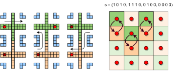
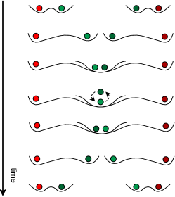
A switchable swap refers to a procedure where two neighboring qubits are physically swapped conditioned on the settings of on-chip switches.
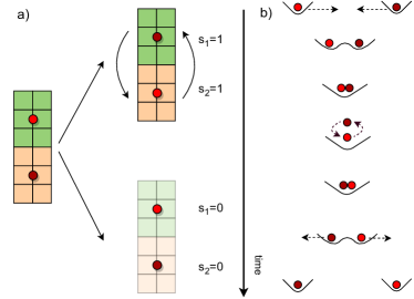
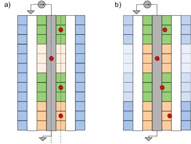
Consider two qubits (1,2) held in separate zones (1,2), as illustrated in Fig. 3 a). Each zone contains dynamic electrodes. We implement a switchable swap as follows. If switches are set to , we connect the dynamic electrodes in both zones to DACs which play waveforms that result in a “swap sequence”, such as shown in Fig. 3 b), which reorders the qubits. On the other hand, if switches are set to , we connect the electrodes to DACs which execute a “stay still” sequence, keeping the qubits in place. This allows implementing a switchable swap using DACs333In this particular example, the number of DACs could be reduced by half by simply leaving the electrodes unconnected whenever we want to execute a “stay still” sequence. Further reduction in DAC could be achieved by wiring the odd and even zones to the same DACs, but with inverted mapping. However, we ignore these tricks in the rest of the paper for the sake of generality. and 2 bits of information444Technically, as and are not valid control words, it suffices to send one bit here. However, controlling every switch individually will become important later, so we assume setting one switch requires one bit of information throughout the paper.
III.2 1D reconfiguration
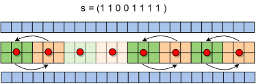
We now enlarge the processor to be a linear repeating array with zones , as illustrated in Fig. 4. Every second zone is connected to the same fixed set of DACs, i.e. if , then every dynamic electrode in zone executes the same waveform as the corresponding dynamic electrode in zone . Thus, by playing the same waveforms as in Sec. III.1, and sending an -bit word to the QPU, we can implement a switchable swap of qubits for every odd in parallel. We call this step an “odd swap”. Similarly, an “even swap” - a switchable swap of qubits for every even in parallel - can be accomplished by playing a different “swap waveform” and sending another -bit word . Implementing an arbitrary odd or even swap in a -qubit array requires DACs, the same as a switchable swap, and bits of information.
As is well known, these odd/even swap primitives suffice to perform arbitrary qubit reconfiguration in 1D using an algorithm known as “odd-even sort” [44]. Specifically, denote the current qubit configuration as , and the target configuration as . In the first time step, qubits and swapped if for every odd . In the second time step step, qubits and swapped if for every even . These steps are repeated until . The odd-even sort is the time-optimal method of sorting qubits in 1D, with a worst-case run time of time-steps.
III.3 2D regular array reconfiguration
Consider a rectangular 2D grid of qubits, where every qubit can be swapped with any of its four neighbors. This corresponds to an ion trap tiled with X-junctions, with one qubit per junction [4]. In this case, qubit swap can still be performed using a swap sequence as in Fig. 3 b). Alternatively, it can be executed as a sequence of shuttling steps as illustrated in Fig. 5 a). Regardless of the physical implementation, we can still consider a switchable qubit swap to be a logical primitive, and the swap can be either horizontal (in a row) or vertical (in a column).
The 1D reconfiguration algorithm can be extended onto a regular 2D grid as follows [45, 46, 47]. Consider a grid of qubits arranged in a 2D array. We enumerate zones as , where and . A zone is considered “odd” if is odd, and “even” otherwise, as shown in Fig. 5 b). We achieve arbitrary qubit reconfiguration as follows. First, we rearrange the qubits in every row in parallel such that, for every column, the target row of every qubit is different, which is always possible thanks to Hall’s marriage theorem [47]. This rearrangement proceeds by horizontal odd-even swap as outlined in Sec. III.2, and thus takes at most time-steps. Afterward, we rearrange the qubits in every column in parallel to place every qubit in the target row. This is executed by vertical odd-even swap and takes at most time steps. Finally, we proceed with the final row-wise rearrangement, which takes at most time steps. Thus, the WISE architecture allows for arbitrary permutation of qubits in 2D in at most time steps555Changing the permutation order to column-row-column allows for arbitrary permutation in at most steps, which is more efficient if and two types of zones.
III.4 Realistic 2D array reconfiguration
The regular 2D array described in Sec. III.3 is not a preferred arrangement of zones for several reasons. First, junctions typically require a larger electrode count and footprint than linear segments. Thus, allocating one junction per qubit may be exceedingly costly, and it will likely be preferable to operate with qubits per junction. Second, quantum computing requires not just an array of individual qubits, but an array of qubit chains to facilitate multi-qubit gates. Thus, any reconfiguration method must consider how qubits come together in larger chains. Finally, a QPU might require specialized zones, such as an “ion loading zones” [48] or “qubit readout zones” [49]. A practical reconfiguration method should thus allow for different zone types.
Fortunately, the methods presented above can be easily extended to such more realistic traps. As an example, consider a 2D ion trap with qubits per junction, configured to perform quantum gates on two-qubit chains stored in “gate zones”. An illustration of the trap and qubits is shown in Fig. 6.
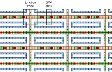
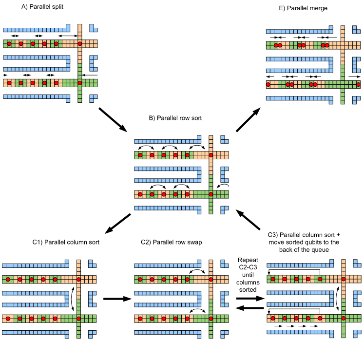
In order to perform arbitrary reconfiguration using a dynamic electrode parallelization, we divide the trap into four zone types – junction odd, junction even, gate odd, gate even – arranged as shown in Fig. 6. Since every odd zone only neighbors even zones, row-wise and column-wise odd-even sort operations remain unchanged. We assume each gate zone contains dynamic electrodes, while a junction zone contains dynamic electrodes [50]. The algorithm for sorting this more realistic trap of qubits using parallel dynamic control is illustrated in Fig. 7. In an array of qubits, each step can be executed by using dynamic DACs and bits of information. The algorithm has an approximate runtime of time steps. Similar techniques can be applied to handle longer chains, different numbers of qubits per junction, and specialized zones.
III.5 Performance
The total duration of qubit reconfiguration depends on the time it takes to execute a single step of parallel swaps. This, in turn, depends on the duration of other primitives, such as ion splitting/merging/rotation/linear shuttling (in case of a 1D swap in Fig. 3 b)) or junction shuttling (in case of a 2D swap in Fig. 5 a)). As an order of magnitude, we assume a qubit swap duration of , which is representative of the capabilities of today’s small-scale quantum computers [51, 52]. However, significantly faster swaps are feasible in the future [19].
Furthermore, in a 2D array, the reconfiguration time depends on the number of zones , as well as on the number of qubits per junction . Finally, the reconfiguration time crucially depends on the target permutation, with longer-range connectivity requiring more reconfiguration steps.
As a pessimistic estimate, we consider the worst-case duration of arbitrary qubit routing. For the algorithm in Sec. III.4, it is easy to verify that, for any given , the reconfiguration time is minimized when and . In that case, arbitrary reconfiguration of an -qubit array requires approximately swap steps.
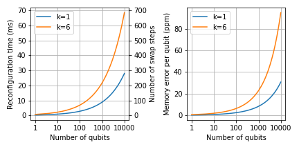
With those assumptions, Fig. 8 (left) shows the maximum time necessary to perform arbitrary qubit routing in a realistic 2D array. We find that, with , we achieve an arbitrary reconfiguration of a 1000-qubit array in ms. To put that in more meaningful terms, we compute the memory error associated with qubit reconfiguration, assuming the error model measured for 43Ca+ clock qubits in [13]. The result is shown in Fig. 8 (right). We find that, for and , we can expect a memory error (per qubit per reconfiguration) of , significantly below two-qubit gate errors in any quantum computing platform today.
This demonstrates that, despite limited freedom of operation, parallel dynamic control is compatible with high-fidelity reconfiguration at scale. At the same time, as each step requires bits of information to specify the switch settings, the overall required data flow rate between the controller and the chip is , which evaluates to Mbit/s for a 1000-qubit chip. It is easy to send this amount of data over a single serial line, offering a major improvement over the standard approach. We emphasize that the numbers in this section describe routing times necessary for arbitrary all-to-all connectivity. In practice, judicious qubit mapping and algorithm choice can significantly decrease the overheads associated with qubit reconfiguration. Furthermore, specific reconfigurations can be executed much faster using less generic routing algorithms.
III.6 Shim electrodes
The quasi-static shim electrodes play a passive role in qubit reconfiguration: they are charged to the desired values before reconfiguration begins, and are disconnected during ion transport. The primary function of shim electrodes is to minimize the stray field offsets between zones such that the same dynamic swap waveform leads to successful qubit swaps in different zones. Among all the transport primitives, ion splitting is typically most sensitive to the stray field setting, requiring axial stray field error of V/m [53]. However, larger stray-field errors can be tolerated as long they are radial. Finally, differences in stray fields can lead to heating and even ion loss during transport operations such as crystal rotations or junction transport. However, these can typically tolerate errors as large as V/m [52].
The second role of shim electrodes is to passively compensate for differences in dynamical electrode moments in different zones, for example, due to fabrication imperfections. While quasi-static shims cannot null out dynamical errors at every point in time, they can be used for fine-tuning the potentials along critical points in a transport trajectory, for example, to prevent frequency crossings during crystal rotations [54].
Future experiments must verify the minimum number of necessary shim electrodes per zone. In subsequent sections, we conservatively assume each zone contains shims888While placing shims per zone increases the number of independent degrees of freedom, this has to be balanced against diminishing effectiveness of further sub-dividing the electrodes.. We anticipate that improvements in control design may allow for as few as shims per zone, controlling 6 degrees of freedom (e.g. 3 field terms and 3 curvature terms) at one point in space during a two-qubit swap.
IV Transport-assisted quantum gates
Consider an -qubit trap, with a global spatially inhomogeneous qubit drive coupling to qubits in all zones. In order to perform transport-assisted quantum gates, we engineer a situation where, for every qubit , the gate Rabi frequency can be adjusted by adjusting the qubit position . There are several different ways this can be implemented in hardware.
For example, one way to implement this scenario is by using integrated microwaves. A simplified case with a linear trap and a single conductor is shown in Fig. 9 a). A trace carrying current along the trap axis creates a magnetic field , near-resonant with the qubit frequency, in every zone in parallel. This leads to qubit coupling with Rabi frequency , where is the distance from the trap axis. Furthermore, it is possible to achieve , for example by exploiting polarization selection rules [55], or using multiple parallel microwave lines [56, 57]. Thus, we obtain , where is a constant. Therefore, single-qubit interactions can be switched off by placing the qubit at and effectively modulated by moving the qubit along [58, 59].
Another way to implement this scenario is using laser light, for example as illustrated in Fig. 9 b). A laser beam, near-resonant with the qubit transition, is coupled into a trap-integrated waveguide [60, 61, 62] and passively split between multiple paths of comparable intensity [63]. Inside each zone, a grating coupler is used to focus the light near the qubit location at to a spot size [64], which leads to position-dependent Rabi frequency . Thus, single-qubit interactions can be modulated by moving the qubit around , and switched off by placing the qubit at .
IV.1 Dynamic electrode parallelization
We can leverage dynamic electrode parallelization for single-qubit gates, regardless of the implementation, as follows. We set up the dynamic waveforms such that, when , the qubit in zone is moved to position with Rabi frequency . On the other hand, if , the qubit is moved to position where . An illustration of the scenario is shown in Fig. 10 a).
With the drive resonant with the qubit frequency, this generates a Hamiltonian , where , is the global drive phase, and is the global drive strength. If the drive is detuned from the qubit transition frequencies by , we instead obtain a Hamiltonian [65].
Due to unavoidable experimental imperfections, it is impossible to ensure when . Thus qubits in zones with will always experience some residual Rabi frequency . This, if uncorrected, results in infidelity per qubit per gate, which can be a challenge for transport-assisted gates. We mitigate this error using a two-step approach. First, we make use of any knowledge of to coherently undo undesired rotations with subsequent operations. Second, we use composite pulse schemes to cancel out any residual but unknown systematic errors. Using the SK1 pulse sequence [66], for example, one can achieve single-qubit gate infidelities with addressing imperfections as large as , which is readily achievable in practice [67, 68, 69]
In addition to single-qubit gates, dynamic electrode parallelization allows us to switch two-qubit interactions on- and off. When the global drive is turned on to generate a state-dependent force, we can write the effective entangling interaction between qubits and as . This interaction only occurs if the qubits are in the same potential well999 only implements a global single-qubit rotation when applied to individual qubits, which can be corrected for in subsequent gates. Therefore, we set up dynamical waveforms such that, if , qubits are merged into the same well prior to the two-qubit gate, while if , they remain in separate zones. Thus, we generate a Hamiltonian .
Hamiltonians and implement single-qubit gates on arbitrary subsets of qubits in parallel, while implements two-qubit gates on arbitrary subsets of qubits in parallel. Together, they can be used to implement a universal primitive gate set [70, 71], and thus universal quantum computation. Explicitly, a quantum circuit is decomposed onto different basis gates, and implemented by using cycles of time steps, each implementing one of gate layers.
IV.2 Shim demultiplexing
While dynamic electrode parallelization can be readily applied to circuits with a small number of basis gates , it is prohibitively costly for circuits with . This creates a challenge in the NISQ regime, where the ability to implement a continuous variable-angle gate set is beneficial [72, 73, 74]. Shim demultiplexing can be used to overcome this limitation of dynamic electrode parallelization by allowing continuous local control of . This leads to the ability to perform different single-qubit gates in parallel.
In this approach, instead of moving the qubits between two fixed positions and , we adjust continuously using demultiplexed shim electrodes, as illustrated in Fig. 10 b). After the shims are set, we turn off the demultiplexer and execute the operation by applying the global qubit drive. The shims are then set to new values before the next gate layer or transport layer.
Thus, shim demultiplexing allows us to implement a Hamiltonian , where is locally adjustable. This executes parallel rotations with locally adjustable angles across the processor using only a global drive. Combined with global two-qubit gates implemented as before, we obtain a powerful toolbox for NISQ algorithms and beyond.
There are several drawbacks associated with transport-assisted gates via shim demultiplexing. First, as electrode voltages have to be adjusted before every gate layer, demultiplexing slows down the effective clock rate of the quantum computer. Second, the lack of local phase control restricts the use of composite pulses to reduce systematic errors. However, local phase control can be restored using demultiplexed integrated IQ mixers, implementing the control scheme proposed in [75].
V Physical implementation
Ion trap fabrication and operation are fundamentally compatible with electronic integration and CMOS processes. However, as discussed in the introduction, care must be applied to issues of power dissipation, footprint, and data flow. Furthermore, low-complexity electronics are preferred given the relative immaturity of cryogenic CMOS design tools. Finally, care must be taken to avoid introducing additional error sources, such as RF pickup or stray fields.
In this section, we sketch out the structures that need to be integrated into the QPU to implement the WISE architecture. We discuss the design and main performance metrics of the dynamic electrode switch network (Sec. V.1) and the shim demultiplexing network (Sec. V.2). We discuss the main error sources, and in Sec. V.3, summarise why the physical implementation of the WISE architecture indeed alleviates all the main issues of integrated DACs.
V.1 Dynamic electrode switch network
V.1.1 Switch implementation
The basic building block of the dynamic electrode switch network is shown in Fig. 11.
.
The select bit word is loaded via a serial line into a parallel shift register. Afterwards, the entry is used to select whether the electrode in zone is connected to DAC or . The switch itself is built using two transmission gates, each implemented using an NMOS/PMOS transistor pair and an inverter. The DAC outputs are predominantly filtered off-chip.
V.1.2 Switch network
While in principle one switchable electrode per zone suffices to implement a switchable swap (Appendix B) the most flexible wiring is illustrated in Fig. 12, where all dynamic electrodes in every one of zones are connected to switches. This allows for maximum flexibility in the waveform design, as every action can have a completely separate custom waveform set. As all the switches in zone are controlled by the same digital line , the length of the bit select word is .
Since each electrode is always connected to at least one DAC, there is no requirement to integrate capacitors, as off-chip capacitors suffice to provide a DC electrode RF ground. If necessary, residual RF pickup on dynamic electrodes can be reduced by optimizing transmission gate resistance.
V.1.3 Operation timing
The switch network is operated as follows. Consider a single operation step, either a swap (duration ) or a transport-assisted gate (duration ). While the DACs are playing the required waveforms, the word of length bits describing the next transport step is loaded through a serial link into a parallel register. At the end of the transport step, the DAC voltages are set such that , i.e. each electrode is at the same voltage regardless of the switch setting. Then, data from the parallel register is transferred onto the switches101010Note that setting the switches does not affect electrode voltages, thus does not heat the ions., and the next transport step begins. Thus, assuming , as long as the interface supports a data rate of more than , the switch network does not bottleneck the device performance. With as in Sec. III.5, we find that the required data flow rate is kbit/s. Thus, a single serial line with a bandwidth of Mbit/s suffices for qubits.
V.2 Shim demultiplexing
V.2.1 Demultiplexing network
A high-level illustration of the shim demultiplexing network is shown in Fig. 13 a). The QPU consists of multiple analog demultiplexers that serve to connect the shim DAC to the shim electrodes one at a time. A single on/off signal clocks all the demultiplexers on the QPU. Each shim electrode is connected to an integrated capacitor after the demultiplexer.
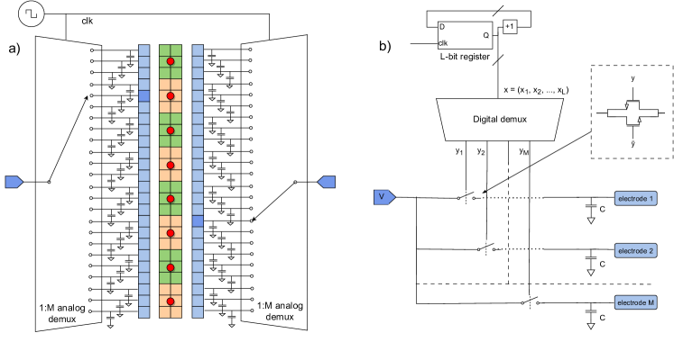
Fig. 13 b) illustrates the demultiplexer circuit in more detail. On every clock cycle, on-chip digital logic increments an -bit register by one, starting from . The output of the register is sent to a digital demultiplexer with outputs. The circuit sets the output , while the rest of its outputs are set to 0. Demultiplexer outputs act as switch control signals, connecting the shim DAC to electrode iff . The individual switches are implemented as transmission gates as before.
After the switch is closed, we wait for time , allowing the electrode to charge, and then advance the clock by one cycle. The procedure is repeated in total times, charging shim electrodes in time using DACs and a single clock line. When , and all the electrodes are charged, we pause the clock signal and execute the subsequent operation layer with shim electrodes floating.
V.2.2 Integrated capacitors
Operation with floating electrodes requires integrated capacitors to provide an RF ground. To make the design practical, capacitances must be sufficiently small to avoid footprint bottlenecks highlighted for integrated DACs.
When disconnected, the voltage on each shim electrode oscillates with amplitude , where is the voltage on the RF electrode, and is a parasitic capacitance between the RF and the shim electrode, and is the capacitance of the integrated capacitor. This leads to additional micromotion, especially if there are variations of between electrodes.
Consider zones of area , each containing shim electrodes, each connected to a capacitor of area . As long as , the capacitors do not represent a significant bottleneck on the device size. Thin-film planar capacitors allow for [28]. Thus, a capacitor with dimensions provides a capacitance of pF. Assuming , we can connect shims per zone to such capacitors without increasing device footprint. Assuming V and fF [36], we expect an RF pickup of mV. This should be sufficient for high-fidelity quantum operations, especially since the pickup can be very uniform with integrated capacitors. If necessary, RF pickup can be further reduced by using larger values of , e.g. by increasing device footprint, increasing the number of capacitor layers, or by using vertical trench capacitors [76, 28].
V.2.3 Timing and I/O count
The shim demultiplexing architecture allows us considerable freedom in trading off the shim charging speed, network complexity, performance, and the number of inputs. Increasing the multiplexing order decreases the number of shim DACs but increases the shim charging time , slowing down the effective clock speed of the quantum computer. While decreasing the electrode charging time directly improves the clock speed, this must be traded off against the additional design and fabrication complexity of high-speed electronics. In addition, faster electrode charging can lead to additional motional excitation of ions, necessitating subsequent recooling. Finally, depending on the number of primitive gates , single-qubit operations will either be executed using dynamic electrode parallelization (which doesn’t require frequent shim recharging), or shim demultiplexing (which requires shim recharging between every gate layer).
As an example, consider a -qubit chip with shims per zone, reconfiguration time ms and transport-assisted gate layers between reconfiguration steps, each requiring all shim electrodes to be recharged. Using a charging time of and , the shim charging time is = . Thus, shim charging takes of system time – significant, but not a runtime bottleneck. At the same time, the total of shim electrodes will require shim voltage inputs, easily achievable in today’s systems. Finally, the charging time of is long enough to not introduce significant electronics design challenges, and to limit motional excitation of the ions.
V.2.4 Voltage errors
In our architecture, shim voltage errors can arise on top of errors from the DAC. The three main sources are charge injection, electrode discharging, and the photoelectric effect.
Charge injection refers to an additional voltage that appears once the switch is opened due to the redistribution of charge accumulated on the control transistors. This results in a fractional voltage shift of , where is the transistor gate-source capacitance. Assuming shim capacitance pF, transistor capacitance fF, and typical shim stray field V/m [76], the charge injection effect is at the level of V/m. The effect is expected to be systematic, and thus compensatable by calibration. Furthermore, the magnitude of charge injection can be reduced by reducing through advanced fabrication processes.
Electrode discharging means electrode voltage decays over time once the switch is opened. The main loss channels are due to current flow through the capacitor and the transistor. We will assume the combined decay time constant of s, based on results reported in [41] for cryogenic transistors and thin-film alumina capacitors of comparable values.
To evaluate the effect of electrode discharging on quantum operations, consider once again a qubit chip with reconfiguration time ms (as in Sec. III.5) and two-qubit gate time . Assuming once again V/m, we find a shim field drift of mV/m during reconfiguration, sufficient for low-heating transport. The most stringent requirement on electrode voltage stability is that stray field drifts can lead to gate mode frequency drifts, causing two-qubit gate errors. During a two-qubit gate, we expect a stray field drift mV/m. Assuming gate mode anharmonicity of kHz per V/m [77], this corresponds to motional frequency drift of Hz, resulting in a negligible two-qubit gate error of [78]. Thus, we expect that electrode discharging will not bottleneck either qubit reconfiguration or quantum gate fidelity111111Also note that it is in principle possible to keep track of these decaying fields and apply appropriate corrections to the drive fields.
Due to the photoelectric effect, the voltage held on the shim electrode – and hence the corresponding stray field – is perturbed by laser light. This effect is most pronounced for short-wavelength light (blue and ultraviolet), but can be meaningful for longer-wavelength radiation as well [79]. The impact of the photoelectric effect can be minimized by carefully managing laser scatter and electrode contamination, as well as by using laser-free gates instead of laser-based gates.
V.3 Comparison to integrated DACs
In a nutshell, our solution replaces the problem of integrating filtered DACs with the problem of integrated switches and small capacitors. Thus, it is only a reasonable solution if the latter issue is easier than the former. Fortunately, as highlighted earlier in the section, our architecture alleviates all the main concerns of integrated DACs:
-
1.
Power dissipation. Unlike a DAC, a transmission-gate switch results in negligible additional power consumption.
-
2.
Data bandwidth. Unlike a DAC, a transmission-gate switch requires only a single bit of information per operation. Thus, the data streaming rate is reduced to kbit/s per zone, allowing for a large number of switches with a single serial line.
-
3.
Footprint. Unlike a DAC, a transmission-gate switch requires a footprint only a few times larger than a single transistor. The transistor size, in turn, depends on the required voltage level, as well as the details of the fabrication process. Assuming a transmission gate footprint of , realistic for V logic levels [80], we find that the switching networks introduce little-to-no overheads on the device footprint (Appendix A). Furthermore, all large DAC filter capacitors (with typical values of nF) are placed off-chip in our architecture. While WISE architecture requires integrated capacitors to eliminate RF pickup on shim electrodes, those can be small ( pF), and their footprint manageable ().
All in all, integrating switches at high density is considerably more practical than integrating DACs at high density.
VI Wiring a 1000-qubit chip
Let us now put all the numbers from the previous sections together to discuss the wiring of a 1000-qubit trapped ion quantum computer. Table 1 in Appendix A shows the main system parameters, collected from the previous sections. In this section, we summarise the most important quantities. The result is illustrated in Fig. 14.
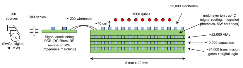
Our device is a 2D array of zones, consisting of gate zones and junction zones. The device holds qubits ( qubits per junction) at a height of um above the surface, in a region of mm (total area ), using dynamic electrodes and shim electrodes. Each shim electrode is connected to one of the pF thin-film planar capacitors, which occupy a total area of on a buried layer. Another buried layer contains the switching network – a total of transmission gates, at an area of – as well as the necessary digital logic.
After the switching network, the dynamic electrodes are connected to off-chip DACs. The shim electrodes are controlled by off-chip DACs via on-chip analog demultiplexers. In addition, electrical connections are required to deliver the digital control signals (with data streaming rate of Mbit/s), power the digital logic, as well as to provide global trapping and qubit drive fields. In total, we use electrical connections between the control electronics and the QPU, comparable to present-day ion trap setups. Additional interconnects will be used for optical wiring (for laser delivery and readout), but the discussion of these is out of the scope of this work.
Quantum operations are performed as interleaved layers of qubit reconfiguration and transport-assisted gates, with arbitrary-angle single-qubit rotations implemented by shim demultiplexing. The reconfiguration takes between (for simple nearest-neighbour routing) and ms (for arbitrary large-scale routing). Quantum gates are enabled by global qubit drives, which implement single-qubit gates in and two-qubit gates in . However, the duration of each transport-assisted gate layer is dominated by the shim charging time of . Depending on the operation, the overall circuit execution speed is therefore between circuit layers per second (for sequential single-qubit gates in identical qubit configuration) and circuit layers per second (for sequential two-qubit gates in maximally different qubit configurations).
VII Summary
We have shown how integrating simple switching electronics into the QPU allows for a 1000-qubit trapped ion quantum computer to be operated with only DACs. The QPU allows for transport-assisted gates, with low errors and effective all-to-all connectivity.
Today’s trapped-ion systems already routinely use DACs per QPU [81]. Furthermore, today’s ion traps are routinely made on silicon substrates [82], with multiple experiments demonstrating compatibility with substrate-integrated passive [83] and active [84, 85] electronics, as well as CMOS processes [86, 87]. Therefore, the proposed design shows that we can increase the scale of trapped-ion quantum computers from today’s qubits to qubits without fundamental roadblocks in electronic wiring. This opens the path to useful NISQ-scale quantum computation with trapped ions.
VII.1 Challenges and open questions
First and foremost, we must verify the feasibility of performing the same transport operations in different trap zones using fixed dynamical waveforms and local shims. This may require optimizing chip fabrication to minimize zone-to-zone variations of electrode moments and to shield stray charges. Second, processor zones and waveforms must be carefully designed to minimize zone-to-zone crosstalk, such that a transport operation in one zone succeeds regardless of the waveform being applied to other zones. If necessary, spacing between zones can be increased without increasing the number of dynamic DACs count using “bucket-brigade” or “conveyor-belt” type shuttling [88, 20, 89, 21, 90]. Third, the RF pickup on the dynamic electrodes caused by finite switch impedance may affect the transport operations in undesirable ways, necessitating the development of low-loss switches or the integration of additional capacitors.
The most important verification of shim demultiplexing is to confirm the stability of voltage offsets caused by charge injection. If problematic, on-chip switches can be miniaturized to reduce transistor capacitance, hence the stored charge. This can, however, lead to increased current leakage, in turn shortening the electrode discharging time. The second assumption that requires verification is that high-fidelity quantum gates can be performed with floating shim electrodes. Finally, experiments should establish realistic timescales for electrode charging, in turn guiding the decision of how many shim electrodes can be connected to a single DAC.
Future experiments must also verify the feasibility of high-fidelity transport-assisted gates. Despite proof-of-principle demonstrations, all highest-fidelity gates in trapped-ion systems were thus far executed with externally modulated localized drives [91, 92, 93]. Further work is needed to demonstrate that precise control over local potentials can be used to overcome zone-to-zone variations, enabling high-fidelity parallel gates. Furthermore, fast and robust calibration procedures must be developed to stabilize local stray-field drifts in larger-scale systems [37].
VII.2 Larger-scale systems
While this paper focused on wiring a 1000-qubit chip, it is interesting to ask if WISE can be applied to larger-scale systems. For example, could a million-qubit chip be wired in the same fashion?
On the face of it, dynamic electrode parallelization can be used to control arbitrarily many qubits from a fixed number of DACs. In practice, this will be limited, for example, by parasitic capacitances of the switches and electrodes and the resulting DAC load swings. Another relevant effect is that the RF pickup on dynamic electrodes connected to one DAC increases in proportion to , affecting the design of DAC filters and, in turn, transport speed.
On the other hand, shim demultiplexing always requires the number of shim DACs and QPU I/O lines to grow in proportion to the qubit number ( in the main text). Scaling the method to requires decreasing the proportionality factor, which can be achieved by a) increasing the multiplexing order above shims per DAC, and b) decreasing the number of shim electrodes per zone to . While the former increases total shim charging time , this is not an issue if the gates are implemented using dynamic electrode multiplexing and if the shim discharging timescales are long. If necessary, can be reduced by decreasing the charging time per electrode , or by sequentially charging additional on-chip capacitors during quantum operations, and then connecting them in parallel to the shim electrodes.
All in all, while WISE can be applied to systems with qubits, the architecture has its limitations which will bound the maximum number of qubits it can efficiently support to some number . Regardless of its precise value (which is difficult to estimate), an -qubit QPU can be then constructed as repeating units of qubits. While DAC and control system integration become necessary for large enough , WISE architecture can nonetheless be employed to significantly reduce the number of DACs per qubit compared to the standard approach, making the power dissipation and footprint issues much more tangible.
To summarize, the WISE architecture opens the door to building trapped-ion quantum computers which are 1–2 orders of magnitude larger than today’s systems. Looking ahead to even larger devices, there are a number of architectural decisions that will significantly impact system wiring. For example, can we reduce the system resource cost if we specialize the WISE architecture for implementing a specific fault-tolerant quantum error-correction code, and if so, which quantum error correction code is optimal [94, 95]? What is the optimal chip size and connectivity for encoding logical qubits [96, 97, 98]? Does the code benefit from long-range connectivity, and if so, of what kind [99, 100, 101]? Regardless of the exact large-scale design, we believe that the methods behind WISE architecture – after thorough refinement in NISQ-scale devices – can serve as its backbone.
We are grateful to the entire team at Oxford Ionics for their support and helpful discussions.
References
- Bharti et al. [2022] K. Bharti, A. Cervera-Lierta, T. H. Kyaw, T. Haug, S. Alperin-Lea, A. Anand, M. Degroote, H. Heimonen, J. S. Kottmann, T. Menke, W.-K. Mok, S. Sim, L.-C. Kwek, and A. Aspuru-Guzik, Noisy intermediate-scale quantum (NISQ) algorithms, Reviews of Modern Physics 94, 015004 (2022).
- Bruzewicz et al. [2019] C. D. Bruzewicz, J. Chiaverini, R. McConnell, and J. M. Sage, Trapped-Ion Quantum Computing: Progress and Challenges, Applied Physics Reviews 6, 021314 (2019).
- Home et al. [2009] J. P. Home, D. Hanneke, J. D. Jost, J. M. Amini, D. Leibfried, and D. J. Wineland, Complete Methods Set for Scalable Ion Trap Quantum Information Processing, Science 325, 1227 (2009).
- Webber et al. [2020] M. Webber, S. Herbert, S. Weidt, and W. K. Hensinger, Efficient Qubit Routing for a Globally Connected Trapped Ion Quantum Computer, Advanced Quantum Technologies 3, 2000027 (2020).
- Rowe et al. [2001] M. A. Rowe, D. Kielpinski, V. Meyer, C. A. Sackett, W. M. Itano, C. Monroe, and D. J. Wineland, Experimental violation of a Bell’s inequality with efficient detection, Nature 409, 791 (2001).
- de Clercq et al. [2016] L. E. de Clercq, H.-Y. Lo, M. Marinelli, D. Nadlinger, R. Oswald, V. Negnevitsky, D. Kienzler, B. Keitch, and J. P. Home, Parallel Transport Quantum Logic Gates with Trapped Ions, Physical Review Letters 116, 080502 (2016).
- Seck et al. [2020] C. M. Seck, A. M. Meier, J. T. Merrill, H. T. Hayden, B. C. Sawyer, C. E. Volin, and K. R. Brown, Single-ion addressing via trap potential modulation in global optical fields, New Journal of Physics 22, 053024 (2020).
- Tinkey et al. [2022] H. N. Tinkey, C. R. Clark, B. C. Sawyer, and K. R. Brown, Transport-Enabled Entangling Gate for Trapped Ions, Physical Review Letters 128, 050502 (2022).
- Wineland et al. [1998] D. J. Wineland, C. Monroe, W. M. Itano, D. Leibfried, B. E. King, and D. M. Meekhof, Experimental Issues in Coherent Quantum-State Manipulation of Trapped Atomic Ions, Journal of Research of the National Institute of Standards and Technology 103, 259 (1998).
- Kielpinski et al. [2002] D. Kielpinski, C. Monroe, and D. J. Wineland, Architecture for a large-scale ion-trap quantum computer, Nature 417, 709 (2002).
- Wang et al. [2021] P. Wang, C.-Y. Luan, M. Qiao, M. Um, J. Zhang, Y. Wang, X. Yuan, M. Gu, J. Zhang, and K. Kim, Single ion qubit with estimated coherence time exceeding one hour, Nature Communications 12, 233 (2021).
- Ruster et al. [2016] T. Ruster, C. T. Schmiegelow, H. Kaufmann, C. Warschburger, F. Schmidt-Kaler, and U. G. Poschinger, A long-lived Zeeman trapped-ion qubit, Applied Physics B 122, 254 (2016).
- Sepiol et al. [2019] M. A. Sepiol, A. C. Hughes, J. E. Tarlton, D. P. Nadlinger, T. G. Ballance, C. J. Ballance, T. P. Harty, A. M. Steane, J. F. Goodwin, and D. M. Lucas, Probing Qubit Memory Errors at the Part-per-Million Level, Physical Review Letters 123, 110503 (2019).
- Pelofske et al. [2022] E. Pelofske, A. Bärtschi, and S. Eidenbenz, Quantum Volume in Practice: What Users Can Expect from NISQ Devices, IEEE Transactions on Quantum Engineering 3, 1 (2022).
- Amini et al. [2010] J. M. Amini, H. Uys, J. H. Wesenberg, S. Seidelin, J. Britton, J. J. Bollinger, D. Leibfried, C. Ospelkaus, A. P. VanDevender, and D. J. Wineland, Toward scalable ion traps for quantum information processing, New Journal of Physics 12, 033031 (2010).
- Sterk et al. [2022] J. D. Sterk, H. Coakley, J. Goldberg, V. Hietala, J. Lechtenberg, H. McGuinness, D. McMurtrey, L. P. Parazzoli, J. Van Der Wall, and D. Stick, Closed-loop optimization of fast trapped-ion shuttling with sub-quanta excitation, npj Quantum Information 8, 1 (2022).
- Pino et al. [2021] J. M. Pino, J. M. Dreiling, C. Figgatt, J. P. Gaebler, S. A. Moses, M. S. Allman, C. H. Baldwin, M. Foss-Feig, D. Hayes, K. Mayer, C. Ryan-Anderson, and B. Neyenhuis, Demonstration of the trapped-ion quantum-CCD computer architecture, Nature 592, 209 (2021).
- Kaushal et al. [2019] V. Kaushal, B. Lekitsch, A. Stahl, J. Hilder, D. Pijn, C. Schmiegelow, A. Bermudez, M. Müller, F. Schmidt-Kaler, and U. Poschinger, Shuttling-Based Trapped-Ion Quantum Information Processing (2019), arxiv:1912.04712 .
- Steane [2006] A. M. Steane, How to build a 300 bit, 1 Giga-operation quantum computer (2006), arxiv:quant-ph/0412165 .
- Alonso et al. [2013] J. Alonso, F. M. Leupold, B. C. Keitch, and J. P. Home, Quantum control of the motional states of trapped ions through fast switching of trapping potentials, New Journal of Physics 15, 023001 (2013).
- Holz [2019] P. Holz, Towards Ion-Lattice Quantum Processors with Surface Trap Arrays, Ph.D. thesis, University of Innsbruck (2019).
- Revelle [2020] M. C. Revelle, Phoenix and Peregrine Ion Traps (2020), arxiv:2009.02398 .
- Holz et al. [2020] P. C. Holz, S. Auchter, G. Stocker, M. Valentini, K. Lakhmanskiy, C. Rössler, P. Stampfer, S. Sgouridis, E. Aschauer, Y. Colombe, and R. Blatt, 2D Linear Trap Array for Quantum Information Processing, Advanced Quantum Technologies 3, 2000031 (2020).
- Stuart et al. [2019] J. Stuart, R. Panock, C. D. Bruzewicz, J. A. Sedlacek, R. McConnell, I. L. Chuang, J. M. Sage, and J. Chiaverini, Chip-integrated voltage sources for control of trapped ions, Physical Review Applied 11, 024010 (2019).
- Guise et al. [2014] N. D. Guise, S. D. Fallek, H. Hayden, C.-S. Pai, C. Volin, K. R. Brown, J. T. Merrill, A. W. Harter, J. M. Amini, L. M. Lust, K. Muldoon, D. Carlson, and J. Budach, In-Vacuum Active Electronics for Microfabricated Ion Traps, Review of Scientific Instruments 85, 063101 (2014).
- Sin [2022] Sinara Fastino wiki (2022).
- Bardin et al. [2019] J. C. Bardin, E. Jeffrey, E. Lucero, T. Huang, S. Das, D. T. Sank, O. Naaman, A. E. Megrant, R. Barends, T. White, M. Giustina, K. J. Satzinger, K. Arya, P. Roushan, B. Chiaro, J. Kelly, Z. Chen, B. Burkett, Y. Chen, A. Dunsworth, A. Fowler, B. Foxen, C. Gidney, R. Graff, P. Klimov, J. Mutus, M. J. McEwen, M. Neeley, C. J. Neill, C. Quintana, A. Vainsencher, H. Neven, and J. Martinis, Design and Characterization of a 28-nm Bulk-CMOS Cryogenic Quantum Controller Dissipating Less Than 2 mW at 3 K, IEEE Journal of Solid-State Circuits 54, 3043 (2019).
- Allcock et al. [2012] D. T. C. Allcock, T. P. Harty, H. A. Janacek, N. M. Linke, C. J. Ballance, A. M. Steane, D. M. Lucas, R. L. Jarecki Jr., S. D. Habermehl, M. G. Blain, D. Stick, and D. L. Moehring, Heating rate and electrode charging measurements in a scalable, microfabricated, surface-electrode ion trap, Applied Physics B 107, 913 (2012).
- Romaszko et al. [2020] Z. D. Romaszko, S. Hong, M. Siegele, R. K. Puddy, F. R. Lebrun-Gallagher, S. Weidt, and W. K. Hensinger, Engineering of microfabricated ion traps and integration of advanced on-chip features, Nature Reviews Physics 2, 285 (2020).
- Blain et al. [2021] M. G. Blain, R. Haltli, P. Maunz, C. D. Nordquist, M. Revelle, and D. Stick, Hybrid MEMS-CMOS ion traps for NISQ computing, Quantum Science and Technology 6, 034011 (2021).
- Walther et al. [2012] A. Walther, F. Ziesel, T. Ruster, S. T. Dawkins, K. Ott, M. Hettrich, K. Singer, F. Schmidt-Kaler, and U. Poschinger, Controlling Fast Transport of Cold Trapped Ions, Physical Review Letters 109, 080501 (2012).
- Bowler et al. [2012] R. Bowler, J. Gaebler, Y. Lin, T. R. Tan, D. Hanneke, J. D. Jost, J. P. Home, D. Leibfried, and D. J. Wineland, Coherent Diabatic Ion Transport and Separation in a Multizone Trap Array, Physical Review Letters 109, 080502 (2012).
- Kaufmann et al. [2014] H. Kaufmann, T. Ruster, C. T. Schmiegelow, F. Schmidt-Kaler, and U. G. Poschinger, Dynamics and control of fast ion crystal splitting in segmented Paul traps, New Journal of Physics 16, 073012 (2014).
- Ruster et al. [2014] T. Ruster, C. Warschburger, H. Kaufmann, C. T. Schmiegelow, A. Walther, M. Hettrich, A. Pfister, V. Kaushal, F. Schmidt-Kaler, and U. G. Poschinger, Experimental realization of fast ion separation in segmented Paul traps, Physical Review A 90, 033410 (2014).
- Kaufmann et al. [2017] H. Kaufmann, T. Ruster, C. T. Schmiegelow, M. A. Luda, V. Kaushal, J. Schulz, D. von Lindenfels, F. Schmidt-Kaler, and U. G. Poschinger, Fast ion swapping for quantum-information processing, Physical Review A 95, 052319 (2017).
- Doret et al. [2012] S. C. Doret, J. M. Amini, K. Wright, C. Volin, T. Killian, A. Ozakin, D. Denison, H. Hayden, C.-S. Pai, R. E. Slusher, and A. W. Harter, Controlling trapping potentials and stray electric fields in a microfabricated ion trap through design and compensation, New Journal of Physics 14, 073012 (2012).
- Nadlinger et al. [2021] D. P. Nadlinger, P. Drmota, D. Main, B. C. Nichol, G. Araneda, R. Srinivas, L. J. Stephenson, C. J. Ballance, and D. M. Lucas, Micromotion minimisation by synchronous detection of parametrically excited motion (2021), arxiv:2107.00056 .
- Kienzler [2015] D. Kienzler, Quantum Harmonic Oscillator State Synthesis by Reservoir Engineering, Doctoral Thesis, ETH Zurich (2015).
- Decaroli [2021] C. Decaroli, Multi-Wafer Ion Traps for Scalable Quantum Information Processing, Doctoral Thesis, ETH Zurich (2021).
- Alonso et al. [2016] J. Alonso, F. M. Leupold, Z. U. Solèr, M. Fadel, M. Marinelli, B. C. Keitch, V. Negnevitsky, and J. P. Home, Generation of large coherent states by bang–bang control of a trapped-ion oscillator, Nature Communications 7, 11243 (2016).
- Xu et al. [2020] Y. Xu, F. K. Unseld, A. Corna, A. M. J. Zwerver, A. Sammak, D. Brousse, N. Samkharadze, S. V. Amitonov, M. Veldhorst, G. Scappucci, R. Ishihara, and L. M. K. Vandersypen, On-chip integration of Si/SiGe-based quantum dots and switched-capacitor circuits, Applied Physics Letters 117, 144002 (2020).
- Brownnutt et al. [2015] M. Brownnutt, M. Kumph, P. Rabl, and R. Blatt, Ion-trap measurements of electric-field noise near surfaces, Reviews of Modern Physics 87, 1419 (2015).
- Talukdar et al. [2016] I. Talukdar, D. J. Gorman, N. Daniilidis, P. Schindler, S. Ebadi, H. Kaufmann, T. Zhang, and H. Häffner, Implications of surface noise for the motional coherence of trapped ions, Physical Review A 93, 043415 (2016).
- Wik [2022] Wikipedia: Odd-even sort (2022).
- Alon et al. [1994] N. Alon, F. R. K. Chung, and R. L. Graham, Routing Permutations on Graphs via Matchings, SIAM Journal on Discrete Mathematics 7, 513 (1994).
- Childs et al. [2019] A. M. Childs, E. Schoute, and C. M. Unsal, Circuit Transformations for Quantum Architectures (2019), arxiv:1902.09102 .
- Banerjee et al. [2022] A. Banerjee, X. Liang, and R. Tohid, Locality-aware Qubit Routing for the Grid Architecture (2022), arxiv:2203.11333 .
- Shi et al. [2023] X. Shi, S. L. Todaro, G. L. Mintzer, C. D. Bruzewicz, J. Chiaverini, and I. L. Chuang, Ablation loading of barium ions into a surface electrode trap (2023), arxiv:2303.02143 .
- Ghadimi et al. [2017] M. Ghadimi, V. Blūms, B. G. Norton, P. M. Fisher, S. C. Connell, J. M. Amini, C. Volin, H. Hayden, C.-S. Pai, D. Kielpinski, M. Lobino, and E. W. Streed, Scalable ion–photon quantum interface based on integrated diffractive mirrors, npj Quantum Information 3, 1 (2017).
- Zhang et al. [2022] C. Zhang, K. K. Mehta, and J. P. Home, Optimization and implementation of a surface-electrode ion trap junction, New Journal of Physics 24, 073030 (2022).
- Bermudez et al. [2017] A. Bermudez, X. Xu, R. Nigmatullin, J. O’Gorman, V. Negnevitsky, P. Schindler, T. Monz, U. G. Poschinger, C. Hempel, J. Home, F. Schmidt-Kaler, M. Biercuk, R. Blatt, S. Benjamin, and M. Müller, Assessing the progress of trapped-ion processors towards fault-tolerant quantum computation, Physical Review X 7, 041061 (2017).
- Burton et al. [2022] W. C. Burton, B. Estey, I. M. Hoffman, A. R. Perry, C. Volin, and G. Price, Transport of multispecies ion crystals through a junction in an RF Paul trap (2022), arxiv:2206.11888 .
- Negnevitsky [2018] V. Negnevitsky, Feedback-Stabilised Quantum States in a Mixed-Species Ion System, Doctoral Thesis, ETH Zurich (2018).
- van Mourik et al. [2020] M. W. van Mourik, E. A. Martinez, L. Gerster, P. Hrmo, T. Monz, P. Schindler, and R. Blatt, Coherent rotations of qubits within a surface ion-trap quantum computer, Physical Review A 102, 022611 (2020).
- Weber et al. [2022] M. A. Weber, C. Löschnauer, J. Wolf, M. F. Gely, R. K. Hanley, J. F. Goodwin, C. J. Ballance, T. P. Harty, and D. M. Lucas, Cryogenic ion trap system for high-fidelity near-field microwave-driven quantum logic (2022), arxiv:2207.11364 .
- Ospelkaus et al. [2008] C. Ospelkaus, C. E. Langer, J. M. Amini, K. R. Brown, D. Leibfried, and D. J. Wineland, Trapped-Ion Quantum Logic Gates Based on Oscillating Magnetic Fields, Physical Review Letters 101, 090502 (2008).
- Allcock et al. [2013] D. T. C. Allcock, T. P. Harty, C. J. Ballance, B. C. Keitch, N. M. Linke, D. N. Stacey, and D. M. Lucas, A microfabricated ion trap with integrated microwave circuitry, Applied Physics Letters 102, 044103 (2013).
- Warring et al. [2013] U. Warring, C. Ospelkaus, Y. Colombe, R. Jördens, D. Leibfried, and D. J. Wineland, Individual-Ion Addressing with Microwave Field Gradients, Physical Review Letters 110, 173002 (2013).
- Leu et al. [2023] A. D. Leu, M. F. Gely, M. A. Weber, M. C. Smith, D. P. Nadlinger, and D. M. Lucas, Fast, high-fidelity addressed single-qubit gates using efficient composite pulse sequences (2023), arxiv:2305.06725 .
- Mehta et al. [2020] K. K. Mehta, C. Zhang, M. Malinowski, T.-L. Nguyen, M. Stadler, and J. P. Home, Integrated optical multi-ion quantum logic, Nature 586, 533 (2020).
- Niffenegger et al. [2020] R. J. Niffenegger, J. Stuart, C. Sorace-Agaskar, D. Kharas, S. Bramhavar, C. D. Bruzewicz, W. Loh, R. T. Maxson, R. McConnell, D. Reens, G. N. West, J. M. Sage, and J. Chiaverini, Integrated multi-wavelength control of an ion qubit, Nature 586, 538 (2020).
- Ivory et al. [2021] M. Ivory, W. J. Setzer, N. Karl, H. McGuinness, C. DeRose, M. Blain, D. Stick, M. Gehl, and L. P. Parazzoli, Integrated Optical Addressing of a Trapped Ytterbium Ion, Physical Review X 11, 041033 (2021).
- Vasquez et al. [2023] A. R. Vasquez, C. Mordini, C. Vernière, M. Stadler, M. Malinowski, C. Zhang, D. Kienzler, K. K. Mehta, and J. P. Home, Control of an Atomic Quadrupole Transition in a Phase-Stable Standing Wave, Physical Review Letters 130, 133201 (2023).
- Mehta and Ram [2017] K. K. Mehta and R. J. Ram, Precise and diffraction-limited waveguide-to-free-space focusing gratings, Scientific Reports 7, 2019 (2017).
- Haeffner et al. [2008] H. Haeffner, C. F. Roos, and R. Blatt, Quantum computing with trapped ions, Physics Reports 469, 155 (2008).
- Merrill and Brown [2012] J. T. Merrill and K. R. Brown, Progress in compensating pulse sequences for quantum computation (2012), arxiv:1203.6392 .
- Craik et al. [2017] D. P. L. A. Craik, N. M. Linke, M. A. Sepiol, T. P. Harty, J. F. Goodwin, C. J. Ballance, D. N. Stacey, A. M. Steane, D. M. Lucas, and D. T. C. Allcock, High-fidelity spatial and polarization addressing of Ca-43 qubits using near-field microwave control, Physical Review A 95, 022337 (2017).
- Wang et al. [2020] Y. Wang, S. Crain, C. Fang, B. Zhang, S. Huang, Q. Liang, P. H. Leung, K. R. Brown, and J. Kim, High-fidelity Two-qubit Gates Using a MEMS-based Beam Steering System for Individual Qubit Addressing, Physical Review Letters 125, 150505 (2020).
- Pogorelov et al. [2021] I. Pogorelov, T. Feldker, Ch. D. Marciniak, L. Postler, G. Jacob, O. Krieglsteiner, V. Podlesnic, M. Meth, V. Negnevitsky, M. Stadler, B. Höfer, C. Wächter, K. Lakhmanskiy, R. Blatt, P. Schindler, and T. Monz, Compact Ion-Trap Quantum Computing Demonstrator, PRX Quantum 2, 020343 (2021).
- Barenco et al. [1995] A. Barenco, C. H. Bennett, R. Cleve, D. P. DiVincenzo, N. Margolus, P. Shor, T. Sleator, J. A. Smolin, and H. Weinfurter, Elementary gates for quantum computation, Physical Review A 52, 3457 (1995).
- Nielsen and Chuang [2010] M. A. Nielsen and I. L. Chuang, Quantum Computation and Quantum Information: 10th Anniversary Edition (Cambridge University Press, 2010).
- Bullock and Markov [2003] S. S. Bullock and I. L. Markov, Arbitrary two-qubit computation in 23 elementary gates, Physical Review A 68, 012318 (2003).
- Vatan and Williams [2004] F. Vatan and C. Williams, Optimal Quantum Circuits for General Two-Qubit Gates, Physical Review A 69, 032315 (2004).
- Shende et al. [2004] V. V. Shende, I. L. Markov, and S. S. Bullock, Minimal universal two-qubit controlled-NOT-based circuits, Physical Review A 69, 062321 (2004).
- Srinivas et al. [2022] R. Srinivas, C. M. Löschnauer, M. Malinowski, A. C. Hughes, R. Nourshargh, V. Negnevitsky, D. T. C. Allcock, S. A. King, C. Matthiesen, T. P. Harty, and C. J. Ballance, Coherent Control of Trapped Ion Qubits with Localized Electric Fields (2022), arxiv:2210.16129 .
- Guise et al. [2015] N. D. Guise, S. D. Fallek, K. E. Stevens, K. R. Brown, C. Volin, A. W. Harter, J. M. Amini, R. E. Higashi, S. T. Lu, H. M. Chanhvongsak, T. A. Nguyen, M. S. Marcus, T. R. Ohnstein, and D. W. Youngner, Ball-grid array architecture for microfabricated ion traps, Journal of Applied Physics 117, 174901 (2015).
- Home et al. [2011] J. P. Home, D. Hanneke, J. D. Jost, D. Leibfried, and D. J. Wineland, Normal modes of trapped ions in the presence of anharmonic trap potentials, New Journal of Physics 13, 073026 (2011).
- Malinowski [2021] M. Malinowski, Unitary and Dissipative Trapped-Ion Entanglement Using Integrated Optics, Doctoral Thesis, ETH Zurich (2021).
- Harlander et al. [2010] M. Harlander, M. Brownnutt, W. Hänsel, and R. Blatt, Trapped-ion probing of light-induced charging effects on dielectrics, New Journal of Physics 12, 093035 (2010).
- Stuart [2021] J. M. Stuart, Integrated Technologies and Control Techniques for Trapped Ion Array Architectures, Doctoral Thesis, Massachusetts Institute of Technology (2021).
- Decaroli et al. [2021] C. Decaroli, R. Matt, R. Oswald, C. Axline, M. Ernzer, J. Flannery, S. Ragg, and J. P. Home, Design, fabrication and characterization of a micro-fabricated stacked-wafer segmented ion trap with two X-junctions, Quantum Science and Technology 6, 044001 (2021).
- Cho et al. [2015] D.-I. Cho, S. Hong, M. Lee, and T. Kim, A review of silicon microfabricated ion traps for quantum information processing, Micro and Nano Systems Letters 3, 2 (2015).
- Zhao et al. [2021] P. Zhao, J.-P. Likforman, H. Y. Li, J. Tao, T. Henner, Y. D. Lim, W. W. Seit, C. S. Tan, and L. Guidoni, TSV-integrated Surface Electrode Ion Trap for Scalable Quantum Information Processing, Applied Physics Letters 118, 124003 (2021).
- Reens et al. [2022] D. Reens, M. Collins, J. Ciampi, D. Kharas, B. F. Aull, K. Donlon, C. D. Bruzewicz, B. Felton, J. Stuart, R. J. Niffenegger, P. Rich, D. Braje, K. K. Ryu, J. Chiaverini, and R. McConnell, High-Fidelity Ion State Detection Using Trap-Integrated Avalanche Photodiodes, Physical Review Letters 129, 100502 (2022).
- Setzer et al. [2021] W. J. Setzer, M. Ivory, O. Slobodyan, J. W. Van Der Wall, L. P. Parazzoli, D. Stick, M. Gehl, M. Blain, R. R. Kay, and H. J. McGuinness, Fluorescence Detection of a Trapped Ion with a Monolithically Integrated Single-Photon-Counting Avalanche Diode, Applied Physics Letters 119, 154002 (2021).
- Mehta et al. [2014] K. K. Mehta, A. M. Eltony, C. D. Bruzewicz, I. L. Chuang, R. J. Ram, J. M. Sage, and J. Chiaverini, Ion traps fabricated in a CMOS foundry, Applied Physics Letters 105, 044103 (2014).
- Auchter et al. [2022] S. Auchter, C. Axline, C. Decaroli, M. Valentini, L. Purwin, R. Oswald, R. Matt, E. Aschauer, Y. Colombe, P. Holz, T. Monz, R. Blatt, P. Schindler, C. Rössler, and J. Home, Industrially microfabricated ion trap with 1 eV trap depth, Quantum Science and Technology 7, 035015 (2022).
- Sangster and Teer [1969] F. Sangster and K. Teer, Bucket-brigade electronics: New possibilities for delay, time-axis conversion, and scanning, IEEE Journal of Solid-State Circuits 4, 131 (1969).
- Mills et al. [2019] A. R. Mills, D. M. Zajac, M. J. Gullans, F. J. Schupp, T. M. Hazard, and J. R. Petta, Shuttling a single charge across a one-dimensional array of silicon quantum dots, Nature Communications 10, 1063 (2019).
- Seidler et al. [2022] I. Seidler, T. Struck, R. Xue, N. Focke, S. Trellenkamp, H. Bluhm, and L. R. Schreiber, Conveyor-mode single-electron shuttling in Si/SiGe for a scalable quantum computing architecture, npj Quantum Information 8, 1 (2022).
- Harty et al. [2014] T. P. Harty, D. T. C. Allcock, C. J. Ballance, L. Guidoni, H. A. Janacek, N. M. Linke, D. N. Stacey, and D. M. Lucas, High-fidelity preparation, gates, memory and readout of a trapped-ion quantum bit, Physical Review Letters 113, 220501 (2014).
- Srinivas et al. [2021] R. Srinivas, S. C. Burd, H. M. Knaack, R. T. Sutherland, A. Kwiatkowski, S. Glancy, E. Knill, D. J. Wineland, D. Leibfried, A. C. Wilson, D. T. C. Allcock, and D. H. Slichter, High-fidelity laser-free universal control of two trapped ion qubits, Nature 597, 209 (2021).
- Clark et al. [2021] C. R. Clark, H. N. Tinkey, B. C. Sawyer, A. M. Meier, K. A. Burkhardt, C. M. Seck, C. M. Shappert, N. D. Guise, C. E. Volin, S. D. Fallek, H. T. Hayden, W. G. Rellergert, and K. R. Brown, High-Fidelity Bell-State Preparation with ${̂40}$Ca$+̂$ Optical Qubits, Physical Review Letters 127, 130505 (2021).
- Cohen et al. [2022] L. Z. Cohen, I. H. Kim, S. D. Bartlett, and B. J. Brown, Low-overhead fault-tolerant quantum computing using long-range connectivity, Science Advances 8, eabn1717 (2022).
- Tremblay et al. [2022] M. A. Tremblay, N. Delfosse, and M. E. Beverland, Constant-overhead quantum error correction with thin planar connectivity, Physical Review Letters 129, 050504 (2022).
- Metodi et al. [2005] T. S. Metodi, D. D. Thaker, A. W. Cross, F. T. Chong, and I. L. Chuang, A Quantum Logic Array Microarchitecture: Scalable Quantum Data Movement and Computation, in Proceedings of the 38th Annual IEEE/ACM International Symposium on Microarchitecture, MICRO 38 (IEEE Computer Society, USA, 2005) pp. 305–318.
- Monroe et al. [2014] C. Monroe, R. Raussendorf, A. Ruthven, K. R. Brown, P. Maunz, L.-M. Duan, and J. Kim, Large-scale modular quantum-computer architecture with atomic memory and photonic interconnects, Physical Review A 89, 022317 (2014).
- Nigmatullin et al. [2016] R. Nigmatullin, C. J. Ballance, N. de Beaudrap, and S. C. Benjamin, Minimally complex ion traps as modules for quantum communication and computing, New Journal of Physics 18, 103028 (2016).
- Stephenson et al. [2020] L. J. Stephenson, D. P. Nadlinger, B. C. Nichol, S. An, P. Drmota, T. G. Ballance, K. Thirumalai, J. F. Goodwin, D. M. Lucas, and C. J. Ballance, High-Rate, High-Fidelity Entanglement of Qubits Across an Elementary Quantum Network, Physical Review Letters 124, 110501 (2020).
- Gao et al. [2023] S. Gao, J. A. Blackmore, W. J. Hughes, T. H. Doherty, and J. F. Goodwin, Optimisation of Scalable Ion-Cavity Interfaces for Quantum Photonic Networks, Physical Review Applied 19, 014033 (2023).
- Krutyanskiy et al. [2023] V. Krutyanskiy, M. Galli, V. Krcmarsky, S. Baier, D. A. Fioretto, Y. Pu, A. Mazloom, P. Sekatski, M. Canteri, M. Teller, J. Schupp, J. Bate, M. Meraner, N. Sangouard, B. P. Lanyon, and T. E. Northup, Entanglement of trapped-ion qubits separated by 230 meters, Physical Review Letters 130, 050803 (2023).
Appendix A 1000-qubit system parameter table
A detailed list of parameters of a 1000-qubit system and their derivation is shown in Tab. 1.
| Quantity | Symbol | Formula | Value |
| No. of qubits = No. of zones | 1026 | ||
| No. of qubits per junction | 6 | ||
| Zone count | |||
| No. of junctions zones | 171 | ||
| No. of gate zones | 855 | ||
| No. of dynamic electrodes per gate zone | 10 | ||
| No. of dynamic electrodes per junction zone | 20 | ||
| No. of shim electrodes per zone | 10 | ||
| No. of dynamic electrodes | 11,970 | ||
| No. of shim electrodes | 10,260 | ||
| No. of electrodes | 22, 230 | ||
| Ion height | |||
| Average zone size | |||
| Chip size (active region) | |||
| Total area (active region) | |||
| On-chip capacitance density | 3 | ||
| On-chip capacitor size | |||
| Total area (capacitors) | |||
| Shim capacitance to GND (when floating) | pF | ||
| RF voltage | 100 V | ||
| Shim-to-RF capacitance | 1 fF | ||
| RF voltage on shim electrodes | 3 mV | ||
| No. of dynamic switch settings | 0 or 1, i.e. stay or swap | 2 | |
| No. of dynamic DACs | 120 | ||
| Multiplexing order | 128 | ||
| No. of shim DACs | 81 | ||
| Length of switch select word | 1026 bits | ||
| Serial link data rate | 50 Mbit/s | ||
| Switch select time | |||
| No. of trans. gates per dynamic electrode | 2 | ||
| No. of trans. gates per shim electrode | 1 | ||
| No. of trans. gates | 34200 | ||
| Trans. gate size | |||
| Total area (trans. gates) | |||
| Charging time per shim electrode | |||
| Total shim charging time | |||
| Qubit swap time | |||
| Maximum qubit reconfiguration time | 22 ms | ||
| Transistor capacitance | 30 fF | ||
| Typical shim field | 200 V/m | ||
| Charge injection field systematic | V/m | ||
| Shim discharging time constant | 180 s | ||
| Shim field drift during reconfiguration | 25 mV/m | ||
| Shim field drift during two-qubit gate pulse | 0.1 mV/m | ||
| 1-qubit gate pulse time | |||
| 2-qubit gate pulse time | |||
| Transport-assisted 1-qubit gate time | |||
| Transport-assisted 2-qubit gate time | |||
| Maximum system speed | 2600 layers per second | ||
| Minimum system speed | 40 layers per second |
Appendix B Parallel dynamic control with one switch per zone
The implementation presented in the main text assumes every dynamic electrode is connected to a separate switch. This is a conservative assumption, and it should be in fact possible to only connect some dynamic electrodes to switches while leaving the remainder of dynamic electrodes permanently co-wired. In this section, we present an example implementation of that idea, where every zone features only one switchable electrode.
Consider an extension of the 1D swap waveform between zones shown in Fig. 15. In it, green qubits undergo a swap, but red qubits remain stationary. An alternative way to use this waveform is as follows. Suppose there are only two qubits - one in zone 1, and one in zone 2 - and a switchable “push field” that can be used to push qubits in each zone either left or right. Specifically, if , the qubit in zone is pushed into the green location, while if , it is pushed into the red location. After the switch is set, the waveform is executed. Thus, if , the qubits undergo a swap, while if , they remain in the original order.
This swap waveform can be physically implemented as illustrated in Fig. 16. We use dynamic electrodes co-wired to the same DACs to create a double-well potential (first step of the extended transport waveform) in each zone. At the same time, for each zone, we can select whether the ion is pushed into the red or green well at by applying either positive voltage or negative voltage to one electrode, as illustrated in Fig. 16. Afterward, the dynamic DACs play the remainder of the extended transport waveform. This sequence allows us to locally and digitally select if the ion undergoes a swap or not. Thus, one switch per zone suffices to implement parallel dynamic control. The same method can be used to condition the execution of a 2D swap waveform.
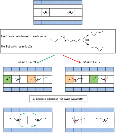
In the basic implementation, the rails connect to separate DACs and are initially set to the same voltage . Once each electrode is connected to one rail, the voltage on the rail is increased to , and the voltage on the rail is reduced to . This ramping can be done smoothly to avoid undesired motional excitation, with DAC outputs filtered off-chip. After all electrodes are set to either or , the swap waveform is played, and the rails return to . This implements one cycle of parallel swaps.
Alternatively, parallel switching can be implemented by purely digital means. In this method, the rails are permanently set to . This can considerably simplify circuit design, and make it compatible with standard digital CMOS. However, a digital implementation may require capacitors after the switches to smooth out the switching impulses. Alternatively, qubits can be displaced with minimum motional excitation and without filtering by a sequence of switching events using bang-bang methods [20, 40].