Helical boundary modes from synthetic spin in a plasmonic lattice
Abstract
Artificial lattices have been used as a platform to extend the application of topological physics beyond electronic systems. Here, using the two-dimensional Lieb lattice as a prototypical example, we show that an array of disks which each support localized plasmon modes give rise to an analog of the quantum spin Hall state enforced by a synthetic time reversal symmetry. We find that an effective next-nearest-neighbor coupling mechanism intrinsic to the plasmonic disk array introduces a nontrivial topological order and gaps out the Bloch spectrum. A faithful mapping of the plasmonic system onto a tight-binding model is developed and shown to capture its essential topological signatures. Full wave numerical simulations of graphene disks arranged in a Lieb lattice confirm the existence of propagating helical boundary modes in the nontrivial band gap.
I Introduction
Artificial lattices can be patterned into ordered structures designed to control efficient flow of energy and informationJoannapoulos2011 . There has been particular interest in developing periodic structures for this purpose that use nontrivial topology in their interior Bloch bandsLu2014a ; Khanikaev2017 . These are known to support protected transport channels at boundaries between distinct topological states in analogy to the well-studied electronic surface states that occur at the boundaries of two and three dimensional topological insulatorsHasan2010 . Indeed, nontrivial bulk Chern bands in two dimensions have been successfully developed on photonicWang2009a , plasmonicJin2017c and even mechanical platformsNash2015 , where time reversal symmetry is broken in order to establish their topological nature. In striking contrast, photonic 2D analogs to quantum spin Hall states which retain time reversal symmetry have been elusive. A key challenge is that the Kramers degeneracies for half-integral angular momentum, whose connectivity is essential for defining the topological state, are generically absent from photonic and plasmonic analogsLu2016 . While multiple realizations of a photonic quantum spin Hall state have been demonstratedHafezi2011 ; Khanikaev2012 ; Wu2015 , intricate engineering via fine tuning of the design is required to enforce the required symmetriesKhanikaev2017 .
In this work we suggest a robust resolution to this dilemma, and illustrate it with studies on a two dimensional plasmonic Lieb latticeWeeks2010 ; Goldman2011 as a prototype. Our model is characterized by two length (energy) scales that express the confinement of excitations within and transmission between nodes of a Lieb lattice network. Over a realizable parameter range in which these scales are of comparable size, we identify both an emergent two-fold Kramers degeneracies and a synthetic spin-orbit process that gaps the Bloch spectra to endow the bands with nontrivial topological orderKane2005a . We test this idea with full wave numerical calculations to confirm the existence of propagating helical modes on the boundaries and we develop a mapping onto a tight binding model that captures the essential spectral signature of this state. We emphasize that these phenomena in artificial lattices are controlled by two energy scales which are tunable over a wide dynamic range and access ordered states that are practically unachievable in ordinary electronic materials. This strategy can be generalized to a wide family of appropriately designed artificial lattices.
II Results and discussion
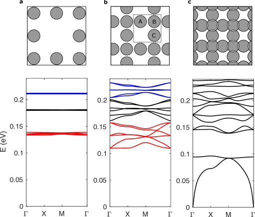
A plasmonic band structure can be calculated when the graphene nanodisks are arranged in a periodic configuration. Here we consider placing graphene nanodisks on a Lieb latticeGoldman2011 . When separation between the disks, , is much larger than the nanodisk diameter, , coupling between the plasmon modes is negligible and we observe a ladder of on-site resonant multipole electromagnetic modes (see fig. 1a). The three groups of energy bands each correspond to the dipole, quadrupole, and hexapole modes of the graphene nanodisk. As the disk separation is decreased, coupling strength between plasmon modes increases and the dispersion in the plasmon band structure becomes stronger. In fig. 1b the plasmon band structure for is shown. Interestingly, we find that the dipole, quadrupole, and hexapole modes develop a non-trivial band structure resembling the band structure of a tight binding Lieb lattice. Finally, when the disks begin to overlap (, fig. 1c), a stark change in the band structure is observed. A low energy hydrodynamic plasmon mode for which the dispersion satisfies as appears and the mapping onto a tight-binding Lieb lattice breaks down. This situation corresponds to the setup given in previous works Silveiro2013 ; Xiong2019 ; Jin2017c ; Jung2018 where periodic modulation of structure or density are used to perturb the hydrodynamic mode.
To better understand the plasmon band structure given in fig. 1b, we develop a mapping of the plasmonic crystal onto a tight-binding model. The governing equations of the plasmonic response can be written as an eigenvalue equation whereJin2017c
| (1) |
The eigenstate is a vector of the potential and current density , is the in-plane momentum operator, is the Coulomb operator, and is the Fermi frequency. The localized plasmonic modes of the nanodisk are analogous to the atomic orbitals in a tight-binding theory. From an eigenmode calculation of the isolated graphene disk, we find that the electric potential is given by
| (2) |
where gives the radial dependence of , is the number of nodes in , and is a positive integer. Here we focus on the six lowest energy modes which have and . Henceforth the superscript will be omitted for notational simplicity. Note that rotational symmetry of the isolated graphene disk implies that and are degenerate in energy. Details on the Hamiltonian and eigenstates are given in the supplementary information.
Equipped with the Hamiltonian and atomic orbitals, we may now calculate the matrix elements of the tight-binding Hamiltonian. In general, the matrix elements between orbitals and on disks separated by are given by
| (3) |
where the inner product is defined such that is a Hermitian eigenproblemJin2017c (see supplementary information for details). Given that we have the current density and electric potential of the orbital modes, it is straightforward to calculate the tight-binding model parameters. For the Lieb lattice, the nearest neighbor (NN) hopping parameters can be calculated by setting or in eq. 3.
We now take a closer look at the nearest neighbor coupling between the quadrupole orbitals . Either by explicit calculation through eq. 3 or by inspection of the mode symmetries, it may be shown that hopping from to given by is zero for . It follows from the symmetry of the quadrupole modes that hopping amplitudes in the and directions will be equal, i.e. for . Finally, it is important to note that the and orbitals have hopping amplitudes with opposite sign. The plasmonic band structure of the quadrupole with nearest neighbor hopping will therefore have two copies of the the 3-band Lieb lattice band structure, where one of the copies will be inverted in energy with respect to the other. This is indeed what we observe for the quadrupole modes as shown in fig. 1b. A similar analysis can be applied to the other multipole modes. Here we will be focusing on the quadrupole mode band structure since it shares the symmetry of the lattice.
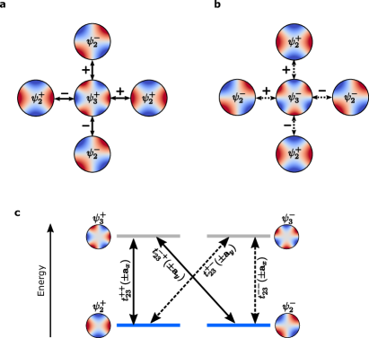
We now extend the model to include orbital coupling between and . Note that the same analysis can be applied to coupling between and . In fig. 2a all allowed hoppings between the and modes are shown along with their respective signs. Hopping parameters , are zero and are not shown. Applying a rotation centered on the mode transforms the configuration of fig. 2a into fig. 2b with an overall sign change on all sites. This transformation directly gives the hopping parameters between and . All the allowed transitions are illustrated on an energy level diagram in fig. 2c.
Considering second order hopping processes mediated by the orbital states, we find two processes that affect the quadrupole mode band structure. First, a second order hopping along two links in the or directions (e.g. followed by ) provides a uniform shift in the energy of all orbital modes. A more interesting effect is found when a left or right turn is made between the first and second hops. Taking into account the signs given in fig. 2, we arrive at an effective second neighbor hopping given by
| (4) |
where , are the nearest neighbor bonds connecting site to , is a creation operator for orbital on lattice site , and is a Pauli matrix acting on the quadrupole orbital degrees of freedom. This intrinsic interaction describing a coupling between the orbitals that is path-dependent is similar to the Kane-Mele spin-orbit interaction discussed in the context of electronic systemsKane2005a . Strength of the interaction can be found by projecting the full Hamiltonian into an effective Hamiltonian in the basis. The effective Bloch Hamiltonian for the orbital basis may then be written as
| (5) |
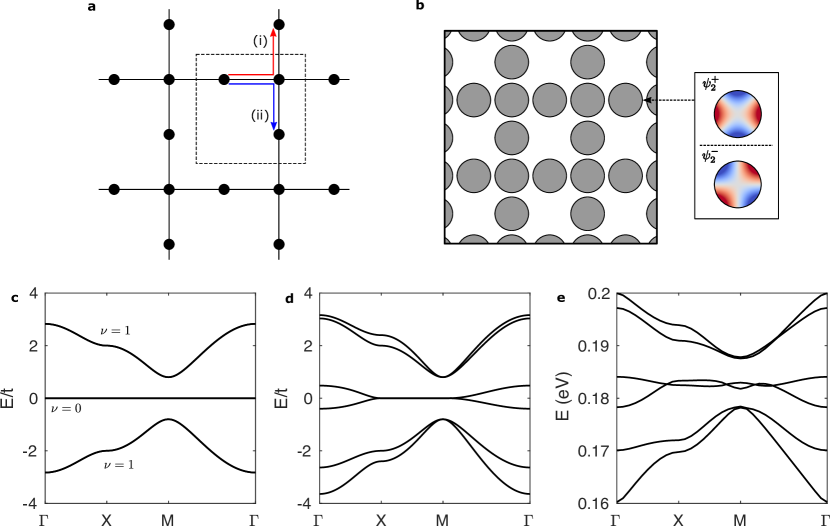
where is the intra-orbital Hamiltonian for orbital , is the ratio between hopping amplitudes and , and is a skew-Hermitian Hamiltonian that describes the effective second neighbor coupling given by eq. 4. Matrix representations of eq. 5 are given in the supplementary information. With the effective Bloch Hamiltonian, we are able to map the quadrupole degrees of freedom of a plasmonic lattice onto a simple tight-binding model with two basis orbitals on each lattice site (see fig. 3a,b).
For the ideal case with in eq. 5, the Hamiltonian may be written as
| (6) |
The band structure for this Hamiltonian is shown in fig. 3c. A strict topological classification of this Hamiltonian based on its symmetries is possible. Define a synthetic time-reversal operator as where is a sublattice symmetry operator acting on the sublattice degrees of freedom, is a Pauli matrix acting on the orbital degrees of freedom, and represents complex conjugation. Then, the Hamiltonian in eq. 6 satisfies . Since , a two-fold degeneracy is enforced at the time reversal invariant momenta by Kramer’s theorem. A particle-hole symmetry operator can also be defined as such that and . From the time-reversal and particle-hole symmetry, we can now place the Hamiltonian into the DIII symmetry classChiu2016 . In two-dimensions, this class is characterized by a topological invariant. Since inversion symmetry is preserved, we may calculate the invariantFu2007a of a single band by
| (7) |
where are the time reversal invariant momenta in the Brillouin zone and is the parity eigenvalue of the band at . Unlike the electronic case for which is given as a product of the parity eigenvalues for all occupied bands, here we associate a separate with each band individually since there is no notion of band filling. The invariant for each band shown in fig. 3c reveals the topologically non-trivial nature of the ideal plasmonic Lieb lattice.
Physically, requires fine tuning to a special state where the symmetry is strictly enforced. The plasmonic lattice comprised of disks does not have symmetries that enforce the condition. When , classification of the system into the DIII class no longer holds and we do not have a sharp definition for the topological invariant. In addition, topologically trivial intra-orbital second neighbor coupling is also present in the plasmonic lattice. Tight-binding calculations for the bulk band structure with and the trivial second neighbor coupling are shown in fig. 3d. Breaking of the synthetic time-reversal symmetry is evident from the lifted degeneracy of the bulk bands at TRIM points and . The spectrum is also no longer symmetric with respect to because particle-hole symmetry is broken by the trivial second neighbor hopping.
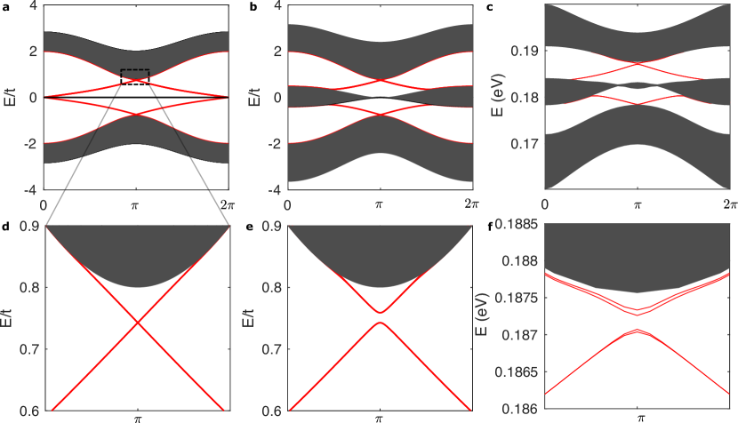
However, by examining the edge states of the physical , we find that the topological signatures of the ideal lattice are still present. The spectrum of the edge modes can be studied in a finite system ribbon geometry and shows that the edge modes from the ideal DIII structure (fig. 4a) survive even when the strict symmetry classification breaks down (fig. 4b). A difference between the two cases is observed at the edge mode crossing points shown in fig. 4d,e where the symmetry broken case shows an avoided crossing originating from mixing of the edge modes. In principle, propagating edge modes near this crossing point will be able to back-scatter. However, the size of the edge mode avoided crossing is roughly two orders of magnitude smaller than the band width, making it negligible in most practical situations. Full wave numerical simulations of the bulk plasmonic band structure shown in fig. 3e confirm that while the condition is not strictly satisfied, the edge modes of topological origin still survive as shown in fig. 4c,f.
To elucidate the properties of the edge modes, we apply a transformation into the angular momentum basis to eq. 5. The angular momentum basis states are given by where the electric potential of is and . Applying the transformation to eq. 5 gives the tight binding Hamiltonian in the angular momentum basis
| (8) |
where and . Written in this form, it is clear that the plasmonic crystal will behave in a similar manner to the electronic quantum spin-hall insulator where the electronic spin degrees of freedom is mapped onto the chirality of the plasmon modes. The plasmonic edge modes observed in fig. 4f will have a potential proportional to on each disk where the chirality is tied to the propagation direction.
The existence of helical edge states can be confirmed by a simulation on a finite array of graphene disks. In order to couple with the angular momentum mode, we use a circularly polarized dipole with dipole moment placed at the edge of an A site graphene disk. Simulation results in fig. 5 show a projection of the excited plasmon fields onto the modes. We find that the dipole strongly couples to a mode which propagates counter-clockwise along the boundaries of the system. A weak excitation of is caused by imperfect coupling between the circularly polarized dipole and the mode.
Finally, we identify two other perturbations that open a topologically trivial gap at the M point and may occur in an array of plasmonic disks. The first is an inversion breaking perturbation which may result from an asymmetric hopping along either the or links in the lattice. A shift of the A or C site plasmonic disk towards the B site will give rise to the inversion breaking perturbation. Shifting the B site energy also opens up a gap on one side of the flat bands. A shift in the Fermi energy of the plasmonic disk will result in this type of perturbation. When applying either of the above mentioned perturbations to an ideal DIII class system, the edge modes are removed only after the gap closes and reopens. Interestingly, even in the physical case where we are no longer in the ideal DIII class, the edge modes persist until the gap is closed, implying that the edge modes remain robust to external perturbations. Results on perturbations are given in the supplementary information.
III Conclusion/Discussion
In summary, we have shown that propagating helical edge modes induced by an intrinsic synthetic spin-orbit process exists in an artificial plasmonic crystal. We consider the Lieb lattice as a prototypical example and develop a mapping of the plasmonic system onto a simple tight-binding model. With the tight-binding model, we identify an ideal limit of the system in which it can be classified into the DIII symmetry class. In this limit, a non-trivial invariant is calculated and the associated topologically protected edge states are shown to exist. It is important to note that this ideal limit is distinct from the case of electron spins on a Lieb lattice and is a result of the opposite sign hopping between the localized plasmon modes. Although the physical plasmonic lattice does not strictly follow the behavior of this ideal limit, we are able to verify that the system is close enough to retain the edge states found for the ideal DIII limit. Propagation of the helical plasmonic edge modes is verified using full wave numerical simulations.
Experimentally, the proposed helical edge modes can be excited by placing a near-field antenna at the edge of the plasmon disk array as shown in fig. 5c. For the setup used in this work, the gap in which the edge mode can be observed is 4meV. We expect the edge mode in this gap to be observable as a plasmonic band gap of similar size has been successfully resolved using the near-field scanning microscope techniqueXiong2019 . The energy scale of the plasmonic band structure can also be shifted by simply scaling the geometry of the lattice (see supplementary information). For a disk size of nm and periodicity nm, the quadrupole band energies are lowered to 70meV. Importantly, the ratio between bandwidth and band gap stays constant as the geometry is scaled. Hence the physical phenomena that we have examined for the setup in this work can be translated to a different energy range by scaling the geometry accordingly.
Methods
All electromagnetic simulations were performed using COMSOL Multiphysics. Graphene is modeled as a surface current with a Drude conductivity, . Scattering time is set to ps where . The bulk plasmonic band structure shown in fig. 1 and fig. 3 was performed by assuming periodic boundary conditions along both the in-plane directions. In the out-of-plane direction, the structure is padded with 1m of free space and a perfectly matched layer of thickness 300nm. The plasmonic band structure calculation for a ribbon geometry shown in fig. 4c,f was performed using a ribbon length of 25 unit cells with periodic boundary conditions only in the direction parallel to the ribbon edges. The circularly polarized dipole used for fig. 5c was placed 5nm above the edge of the graphene nanodisk. Projection of the potential onto the angular momentum states was calculated as for each disk.
Acknowledgements.
SHP, MS and TL acknowledge support by the National Science Foundation, NSF/EFRI Grant No. EFRI-1741660. Work by EJM was supported by the Department of Energy under grant DE-FG02-84ER45118. SHP acknowledges partial support by the National Science Foundation through the University of Minnesota MRSEC under Award Number DMR-2011401.References
- (1) Joannapoulos, J., Johnson, S., Winn, J. & Meade, R. Photonic Crystals: Molding the Flow of Light (Princeton University Press, 2011), 2nd editio edn.
- (2) Lu, L., Joannopoulos, J. D. & Soljačić, M. Topological photonics. Nat. Photonics 8, 821–829 (2014).
- (3) Khanikaev, A. B. & Shvets, G. Two-dimensional topological photonics. Nat. Photonics 11, 763–773 (2017).
- (4) Hasan, M. Z. & Kane, C. L. Colloquium: Topological insulators. Rev. Mod. Phys. 82, 3045–3067 (2010).
- (5) Wang, Z., Chong, Y., Joannopoulos, J. D. & Soljačić, M. Observation of unidirectional backscattering-immune topological electromagnetic states. Nature 461, 772–775 (2009).
- (6) Jin, D. et al. Infrared Topological Plasmons in Graphene. Phys. Rev. Lett. 118, 1–6 (2017).
- (7) Nash, L. M. et al. Topological mechanics of gyroscopic metamaterials. Proc. Natl. Acad. Sci. U. S. A. 112, 14495–14500 (2015).
- (8) Lu, L., Joannopoulos, J. D. & Soljačić, M. Topological states in photonic systems. Nat. Phys. 12, 626–629 (2016).
- (9) Hafezi, M., Demler, E. A., Lukin, M. D. & Taylor, J. M. Robust optical delay lines with topological protection. Nat. Phys. 7, 907–912 (2011).
- (10) Khanikaev, A. B. et al. Photonic topological insulators. Nat. Mater. 12, 233–239 (2012).
- (11) Wu, L. H. & Hu, X. Scheme for achieving a topological photonic crystal by using dielectric material. Phys. Rev. Lett. 114, 1–5 (2015).
- (12) Weeks, C. & Franz, M. Topological insulators on the Lieb and perovskite lattices. Phys. Rev. B 82, 085310 (2010).
- (13) Goldman, N., Urban, D. F. & Bercioux, D. Topological phases for fermionic cold atoms on the Lieb lattice. Phys. Rev. A 83, 063601 (2011).
- (14) Kane, C. L. & Mele, E. J. Z2 Topological Order and the Quantum Spin Hall Effect. Phys. Rev. Lett. 95, 146802 (2005).
- (15) Silveiro, I., Manjavacas, A., Thongrattanasiri, S. & García de Abajo, F. J. Plasmonic energy transfer in periodically doped graphene. New J. Phys. 15, 033042 (2013).
- (16) Xiong, L. et al. Photonic crystal for graphene plasmons. Nat. Commun. 10, 4780 (2019).
- (17) Jung, M., Fan, Z. & Shvets, G. Midinfrared Plasmonic Valleytronics in Metagate-Tuned Graphene. Phys. Rev. Lett. 121, 086807 (2018).
- (18) Chiu, C.-K., Teo, J. C., Schnyder, A. P. & Ryu, S. Classification of topological quantum matter with symmetries. Rev. Mod. Phys. 88, 035005 (2016).
- (19) Fu, L. & Kane, C. L. Topological insulators with inversion symmetry. Phys. Rev. B 76, 045302 (2007).