Periodic Atomic Displacements and Visualization of the Electron-Lattice Interaction in the Cuprate
Abstract
Traditionally, X-ray scattering techniques have been used to detect the breaking of the structural symmetry of the lattice, which accompanies a periodic displacement of the atoms associated with charge density wave (CDW) formation in the cuprate pseudogap states. Similarly, the Spectroscopic Imaging Scanning Tunneling Microscopy (SI-STM) has visualized the short-range CDW. However, local coupling of electrons to the lattice in the form of a short-range CDW has been a challenge to visualize, thus a link between these measurements has been missing. Here, we introduce a novel STM-based technique to visualize the local bond length variations obtained from topographic imaging with picometer precision. Application of this technique to the high- cuprate superconductor Bi2Sr2CaCu2O8+δrevealed a high-fidelity local lattice distortion of the BiO lattice as large as 2. In addition, analysis of local breaking of rotational symmetry associated with the bond lengths reveals modulations around four-unit-cell periodicity in both and representations in the group of the lattice, which coincides with the uni-directional d-symmetry CDW (CDW) previously identified within the CuO2 planes, thus providing direct evidence of electron-lattice coupling in the pseudogap state and a link between the X-ray scattering and STM measurements. Overall, our results suggest that the periodic lattice displacements in E representations correspond to a locally-frozen version of the soft phonons identified by the X-ray scattering measurements, and a fluctuation of the bond length is reflected by the fluctuation of the dCDW formation near the quantum critical point.
- Subject Areas
-
Condensed Matter Physics, Strongly Corrected Materials, Superconductivity
I Introduction
The CuO2 plane is a common crystallographic ingredient among different cuprate families and is the main playground of the electronic system. It determines both the electronic and magnetic characteristic properties, and exhibits instabilities towards states such as antiferromagnetism, -wave superconductivity [1], CDW [2], electronic nematicity [3, 4, 5], and pair density wave (PDW) [6, 7]. Interactions among these states as well as their relationships to the bosonic excitations such as the antiferromagnetic spin fluctuation and the phonon excitations underlie the grand challenge of understanding the mechanism of the cuprate high temperature superconductivity.
One of the key phenomena commonly associated with the cuprate pseudogap state is CDW order, for which a static modulation of the charge appears below or near the pseudogap opening temperature [8, 9]. Such a CDW has been ubiquitously observed in different cuprate families, and the associated period is 3-4 unit cells, depending on the material[2]. SI-STM measurements on Bi2Sr2CaCu2O8+δand Ca2-xNaxCuCl2O2has provided evidence for a unidirectional electronic modulation with -wave symmetry (CDW), in which the charge modulations primarily occur at in-plane Oxygen sites, Ox and Oy, in a fashion such that the changes on these sites are out of phase by [10]. In contrast, X-ray diffraction on different cuprates provides evidence of periodic modulations of the lattice, from which CDW (or charge-stripe) order is inferred[11, 12], while resonant soft-X-ray scattering provides evidence of charge modulations on specific atomic sites [13, 14]. Furthermore, neutron scattering, and resonant inelastic X-ray scattering (RIXS) measurements show a softening of bond-stretching phonons at the wave vector corresponding to charge order [15, 16, 17]. An open question is whether it is possible to detect in real space the lattice modulation associated with the dCDW in Bi2Sr2CaCu2O8+δ. Here we demonstrate a new approach to analyzing local bond-length modulations detected by STM topography and show how they correlate with the electronic modulations measured simultaneously by SI-STM.
Fundamentally, the CuO2 plane is formed by a square lattice of Cu, with Oxygens Ox and Oy bridging Cu atoms along orthogonal directions. In Bi2Sr2CaCu2O8+δthere is an orthorhombic distortion of the lattice along axes at 45° to the Cu-O-Cu bond directions, due to a long-period modulation within the BiO bilayers. The SI-STM measurements are performed after cleaving the sample, which leaves a BiO layer at the surface. The long-period modulation of the BiO layers is well characterized and can be mathematically removed from the topographic image, leaving on average a square lattice of Bi atoms whose positions are expected to correlate with the Cu atoms below them.
II Symmetry of the CuO2 square lattice
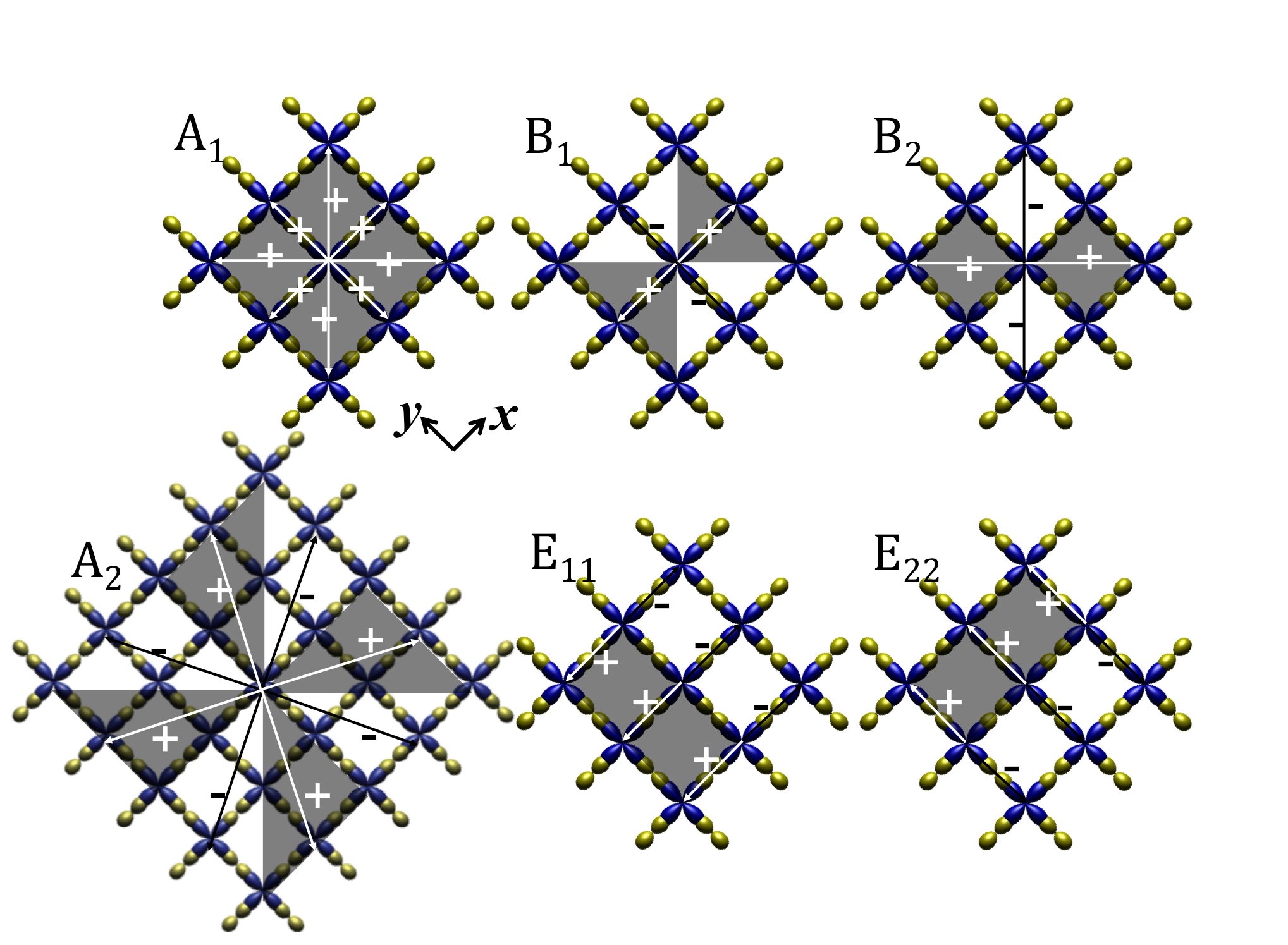
The CuO2 square lattice is group-theoretically classified as a group consisting of 8 symmetry operations, , in which describes a unitary operation, describes an -fold rotation, and describes a mirror operation along the -plane [ () is a mirror plane 45° rotated from -axis]. Irreducible representations of the group are often denoted by , , , , and [18], in which represents a quantity that is invariant under rotation and represents one that changes the sign under the rotation. is a two-dimensional irreducible representation. Ideally, physical quantities within the CuO2 plane are invariant under these operations and are represented by the irreducible representations. However, in a real material, there are impurities, missing atoms, and electronic instabilities coupling to the lattice that would break the underlying symmetry of the lattice. By evaluating symmetries for each irreducible representation with respect to bond lengths about each atomic site, one can test for and characterize the spatial correlations of local lattice distortions.
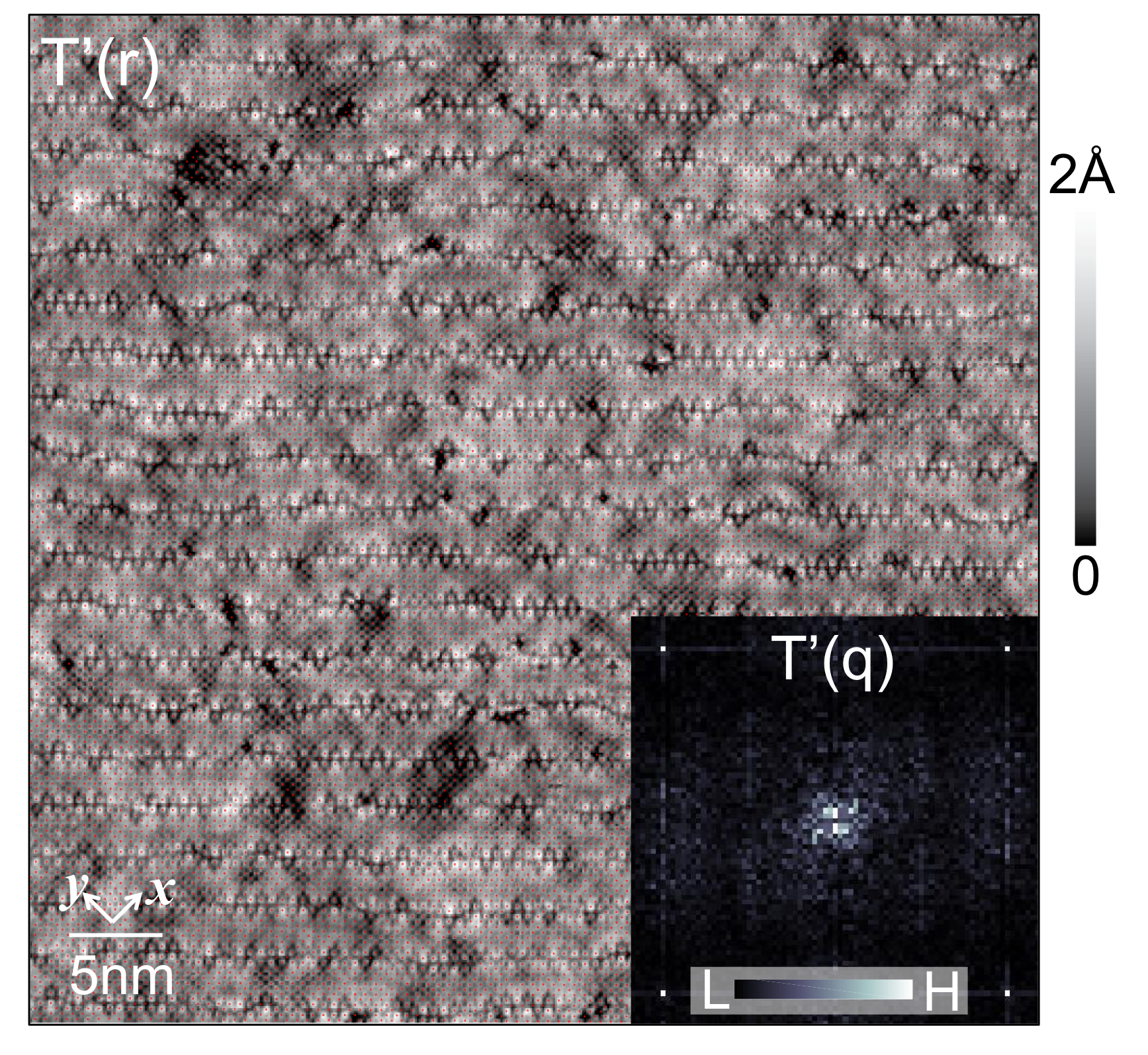
Before such an analysis can be attempted, we must first correct for an experimental artifact. The piezo scanner that controls the STM tip scanning along and directions at a pico-meter precision shows non-linear drifts such that atomic modulations observed in a topography (r) are extrinsically phase disordered. In other words, an observed image of the atoms is not simply described by a sinusoidal wave, but by a combination of cosine and sine waves due to the extrinsic phase disorder. In fact, if the Fourier transform of a raw (r) is evaluated, the Bragg peaks that correspond to periodicities of the atoms show finite intensities in the imaginary part (the sine component of the modulation) because of the tip drifts. Similarly, electronic structure images that are simultaneously taken with the (r), such as current and dI/dV etc, are phase disordered in the same way.
To overcome this systematic error in the measurement, the Lawler-Fujita algorithm [4] has been widely used to remove the effect of the tip drift from images [19, 20, 21]. This algorithm derives a displacement vector field (Fig. 5 in the Appendix section) that describes local phase shifts of a particular modulation (in the present case, atomic modulations) at a coarse-graining length. For the piezo scanner drift, a coarse graining length scale is typically much longer than the atomic spacing (3.83 Å) of the CuO2 unit-cell since relaxation of the piezo scanner occurs very slowly. Here, we use to remove the piezo scanner drift rendering the and any simultaneously taken images to be lattice periodic on average over the 30 Åcoarse graining length (Appendix A: Determination of the atomic sites). To determine the residual (intrinsic) atomic displacements and extract the bond lengths between adjacent Bi atoms, we apply the Lawler-Fujita algorithm once again to obtain the displacement vector field , but now with 6 Å for the coarse graining length. Now, represents how much individual atoms are displaced from the perfect lattice configuration, allowing us to locate Bi positions and possible intrinsic local lattice distortions (Appendix A: Determination of the atomic sites). While the Cu atoms within CuO2 plane are not directly identified as the STM scans over the BiO surface, as we shall show in Fig. 4, electronic structures from the CuO2 layer spatially correlate with structural modulations of the atomic displacements detected at the BiO layer, suggesting that displacements of the Bi atoms reflect those for the Cu atoms within the CuO2.
III Results
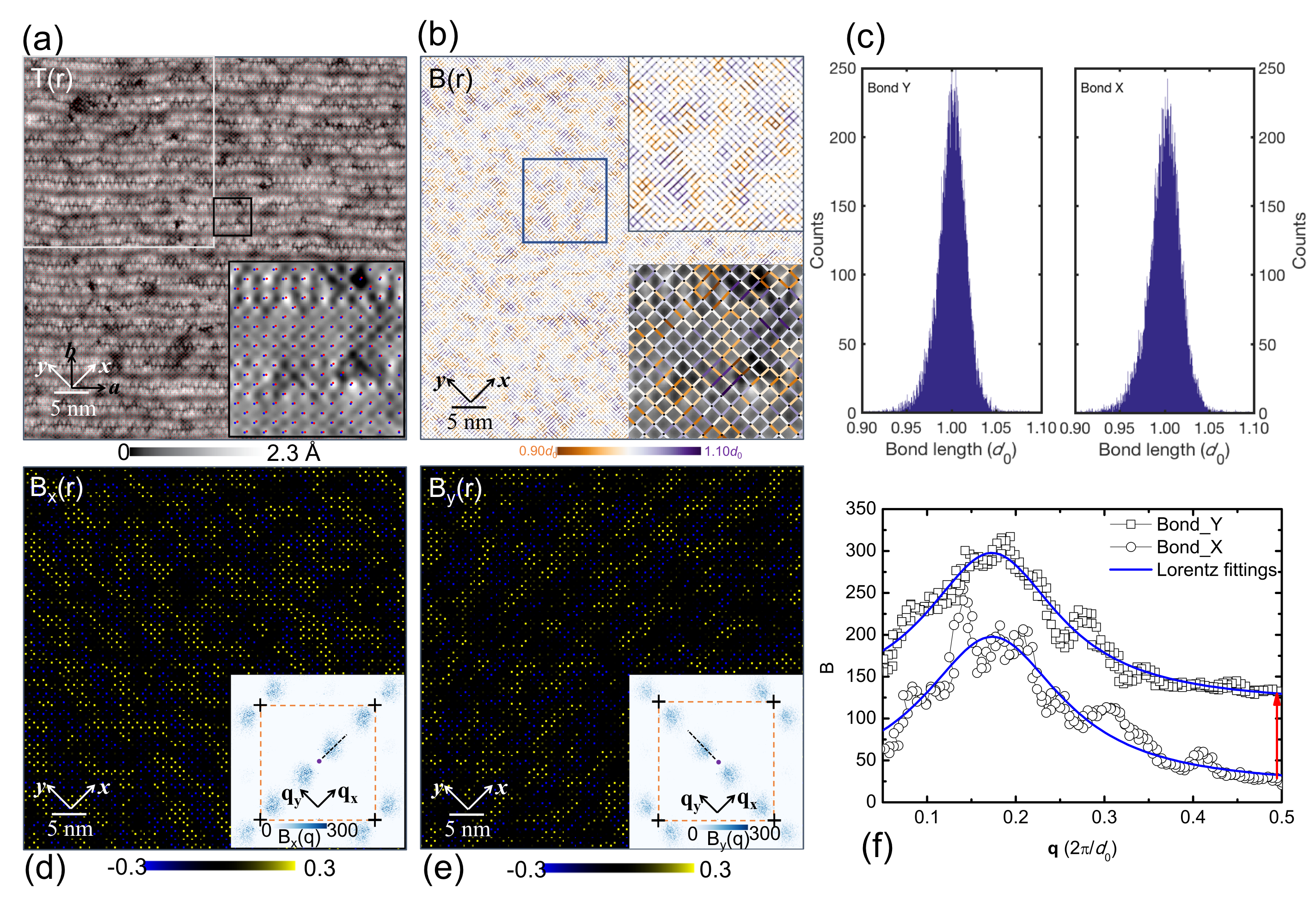
We performed SI-STM measurements at 11 K on a single crystal of Bi2Sr2CaCu2O8+δthat is near optimal doping, with a superconducting transition temperature equal to 91 K (Appendix B: SI-STM Measurements). Figure 1(a) shows a typical drift-corrected topography, , of the Bi2Sr2CaCu2O8+δsample in a 50nm 50nm field of view (FOV). The atoms seen in the (r) are Bi, and the Cu atoms that form the two-dimensional CuO2 plane where all the cuprate phenomenology occurs, are located 6 Å below these Bi atoms. It should be noted that the crystal supermodulation displaces the atoms in the bulk at q= along the b direction. Such an effect is apparently stronger in BiO than in the CuO2 planes[22], masking intrinsic lattice displacements[23]. It is also found that the amplitude of the modulation of the Bi and Cu atoms is, at most, 2 of the Cu-O-Cu bond length 3.83 Å [24]. SI-STM visualizes both the spatial amplitude and phase of the modulation such that the effect of the supermodulation can be effectively removed by Fourier filtration (Fig. 6 of the Appendix section), after which we anticipate that the Cu atom positions can be precisely inferred from the Bi positions. Similarly, the symmetry of the lattice in the CuO2 plane can be obtained by studying the symmetry of the BiO plane that is observed in the . Hence, local lattice distortions of the CuO2 plane can be accessed by studying the corrected topography, .
Now that we know where all the Bi atoms are in , after the filtration of the supermodulation, we show in Fig. 1(b) a bond length map, in which the bond length is represented by a colored bar connecting nearest-neighbor Bi atoms. Small black dots represent the locations of the Bi atoms. It is obvious that the Bi atoms are disordered, exhibiting local displacements from the perfectly periodic positions. Figure 1 (c) shows histograms of the bond lengths for both (right) and (left) directions. Both bond lengths show virtually identical distributions; peak positions (or averages) are located at d0 and the full width at half maximum is about 2 of d0 for both directions. Such disorder is somewhat larger than the estimate from neutron scattering measurements for a stripe-ordered system [25].
Next, we separate the bond lengths according to orientation, associating the bond length between neighboring Bi atoms at ri and rj with the bond center Rij=(+)/2. Note that, geometrically, Rij is approximately the location of the Oxygen sites, Ox and Oy in the CuO2 plane. Figure 1(d) [(e)] is an intensity map of the bond length along the x-direction (y-direction), (r) [(r)]. It is obvious that the bond lengths for both the x and y directions show strong modulations along the Cu-O-Cu directions. The inset in Fig. 1(d) [(e)] is a Fourier transform of the (r) Br), which exhibits a strong peak around Q(0.2,0) [(0, 0.2)] similar to those observed for the electronic density wave in the pseudogap states [26]. The same peaks also appear around the Bragg peaks (marked as “+”), due to the convolution of the lattice and modulations in real space [10]. Line profiles shown in Fig. 1(f) reveal fine structures of these Fourier peaks for both the x and y directions, while the general shape of each line profile can be fitted by a Lorentzian. The fine structure suggests that there would be a domain structure of the bond length modulations having a discommensuration between the domains [27]. These observations obviously show that the translational symmetry of the lattice is broken, which implies an associated modulation of electronic states.
Now, we introduce a symmetry decomposition of the local lattice to analyze possible local breaking of rotational symmetry in the lattice structure. We define a function
| (1) |
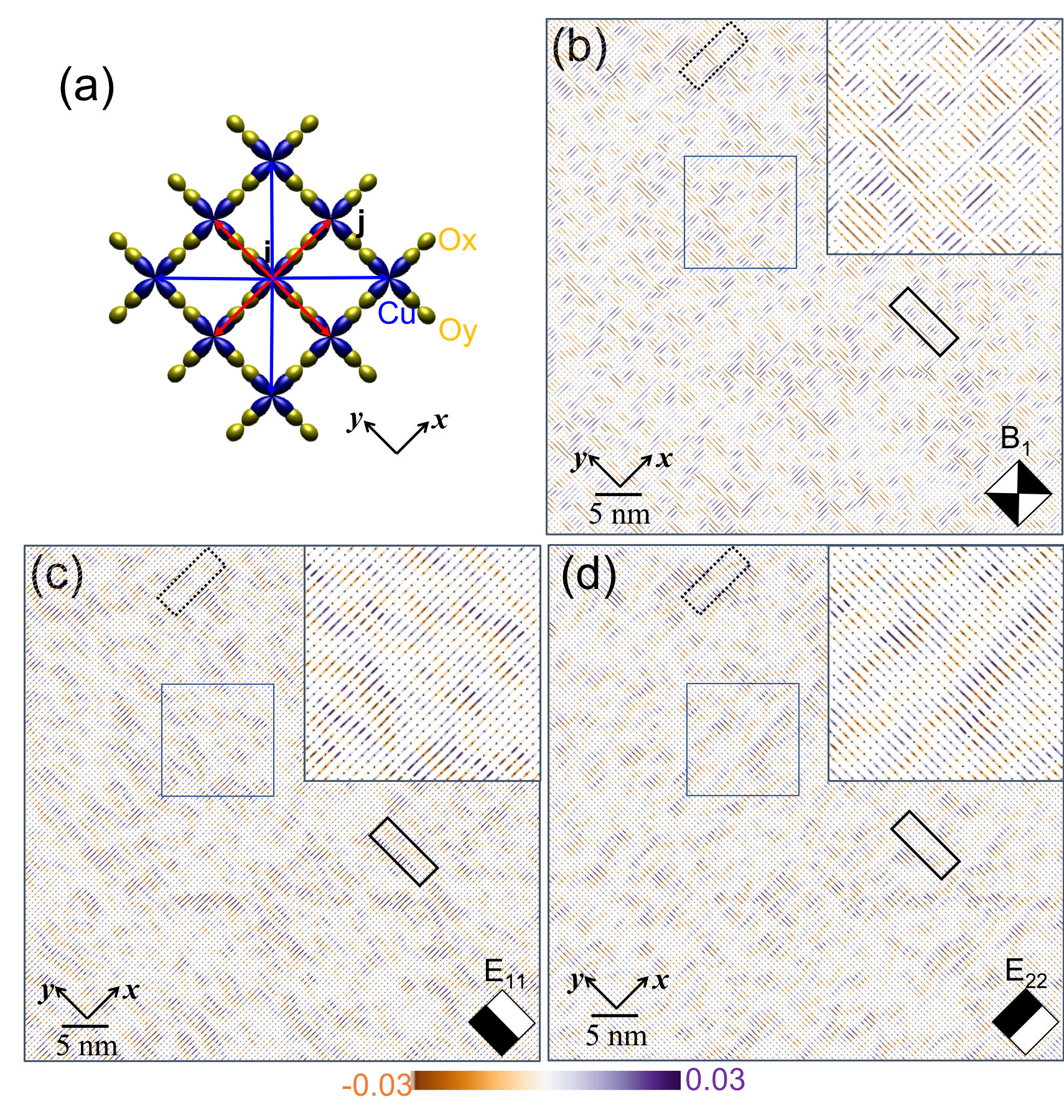
where is an irreducible representation of the group (,,,,), and are positions of the Bi atoms at and sites, respectively, and is a symmetry dependent structure factor. A summation is taken over the nearest-neighbor sites for ,,,, so that is on the scale of and the denominator in eq.(1) is a local average of the bond lengths. (For , the summation is taken over the next-nearest-neighbor sites blue arrows). For example, when we consider the representation of the local bonds,=1 since the representation shows no sign change by the symmetry operations in group (Appendix C: Representation of the group and bond length irreducible representations and Table 1). Then the summation is taken over the nearest-neighbor sites [red arrows in Fig. 2(a)] with the weight . To visualize the irreducible representations of the bonds obtained using eq. (1), we draw a line over the atomic site with a color that represents the intensity obtained by eq. (1). For example, for the representation [Fig. 2(b)], we draw a line along the direction of the expanded bonds[28].
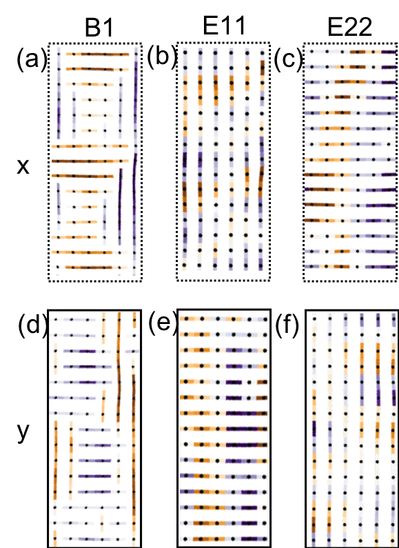
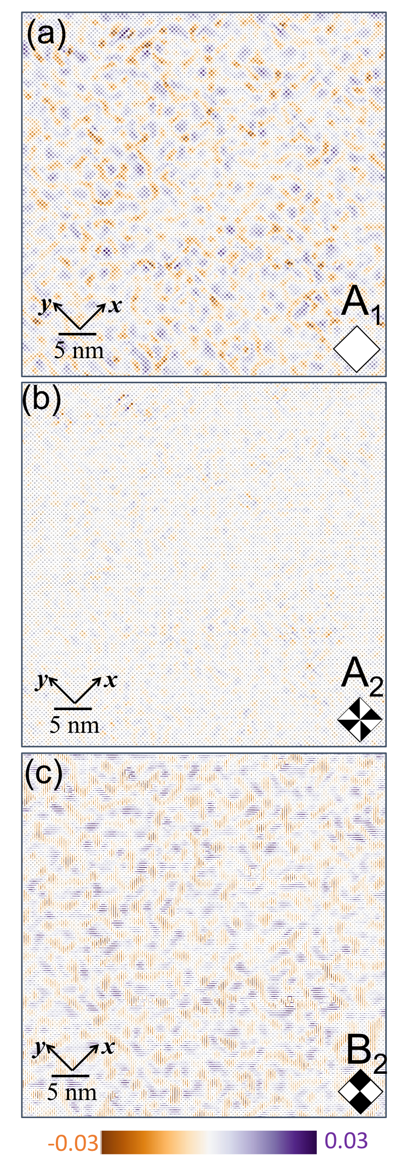
The representation is of particular interest, as it corresponds to a bond stretching quadrupolar mode [15,29]. In Figure 2(b), we show the representation of the bond lengths, in the same FOV as Fig. 1; it exhibits a pattern in which blue and orange bonds alternate at a period of four-unit cells. This can be viewed as a bond “nematicity”. Moreover, a careful examination of the pattern within regions highlighted by the black rectangles in Fig. 2(b) leads us to identify a modulation similar to the unidirectional dCDW that can be seen in the electronic states [Fig. 4(a)]. In fact, the representation is equivalent to -symmetry suggesting that CDW couples to the lattice and locally alters the bond length in a -wave fashion [29].
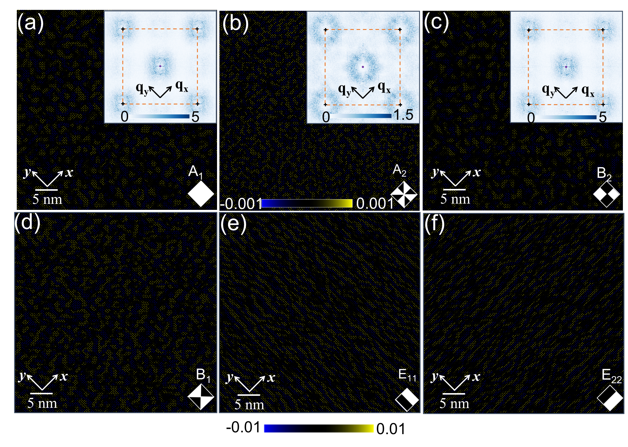
Figures 2(c) and (d) show the (1, 1) and (2, 2) components of the E representation, E11 and , respectively, as given by a 2 x 2 matrix representation. () [ ()] is simply the difference of the bond lengths between nearest neighbor sites of only along the () direction, characterizing a unidirectional stretching or shrinking of the bond length. It is intriguing that both the and representations show spatial modulations of the bond stretching. Similar to the representation shown in Fig. 2(b), a canonical “bond-stretching half-breathing mode” can be found in regions highlighted within the black rectangles again where unidirectional CDW can be clearly observed. Other representations such as , and are shown in the Fig. 8 of Appendix section and discussed in the Appendix C: Representation of the group and bond length irreducible representations.
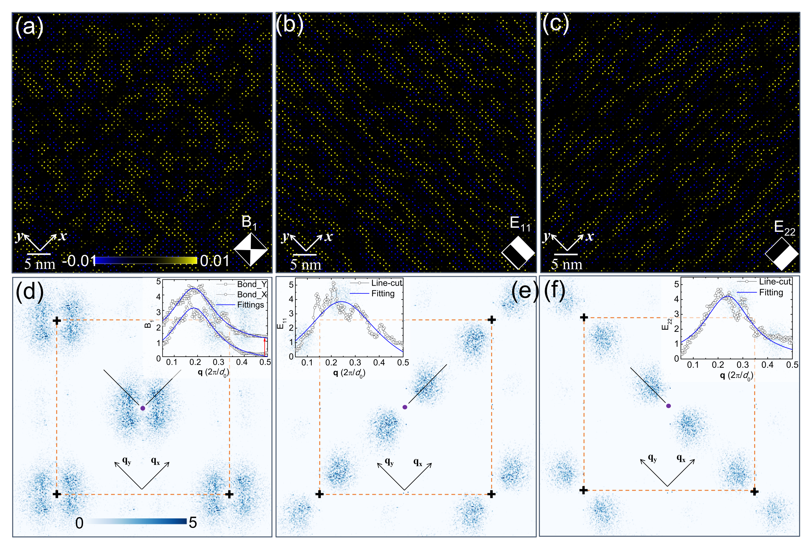
To analyze the modulated structures of each representation of the bond length, shown in Fig.2, we replot () for , , and in Fig.3(a), (b), and (c), respectively, now with amplitude indicated by colored circles. The corresponding Fourier-transform magnitudes are presented in Fig. 3(d), (e), and (f), respectively. For the case of symmetry, the magnitude of the Fourier transform shown in Fig. 3(d) exhibits strong peaks near Q(1/4, 0), (0, 1/4). Note that there are similar peaks surrounding the Bragg peaks marked by the black cross. Similarly, the magnitude Fourier transforms for and , shown respectively in Figs. 3(e) and (f), exhibit strong peaks near the same wavevectors, but only along the Qx or Qy direction.
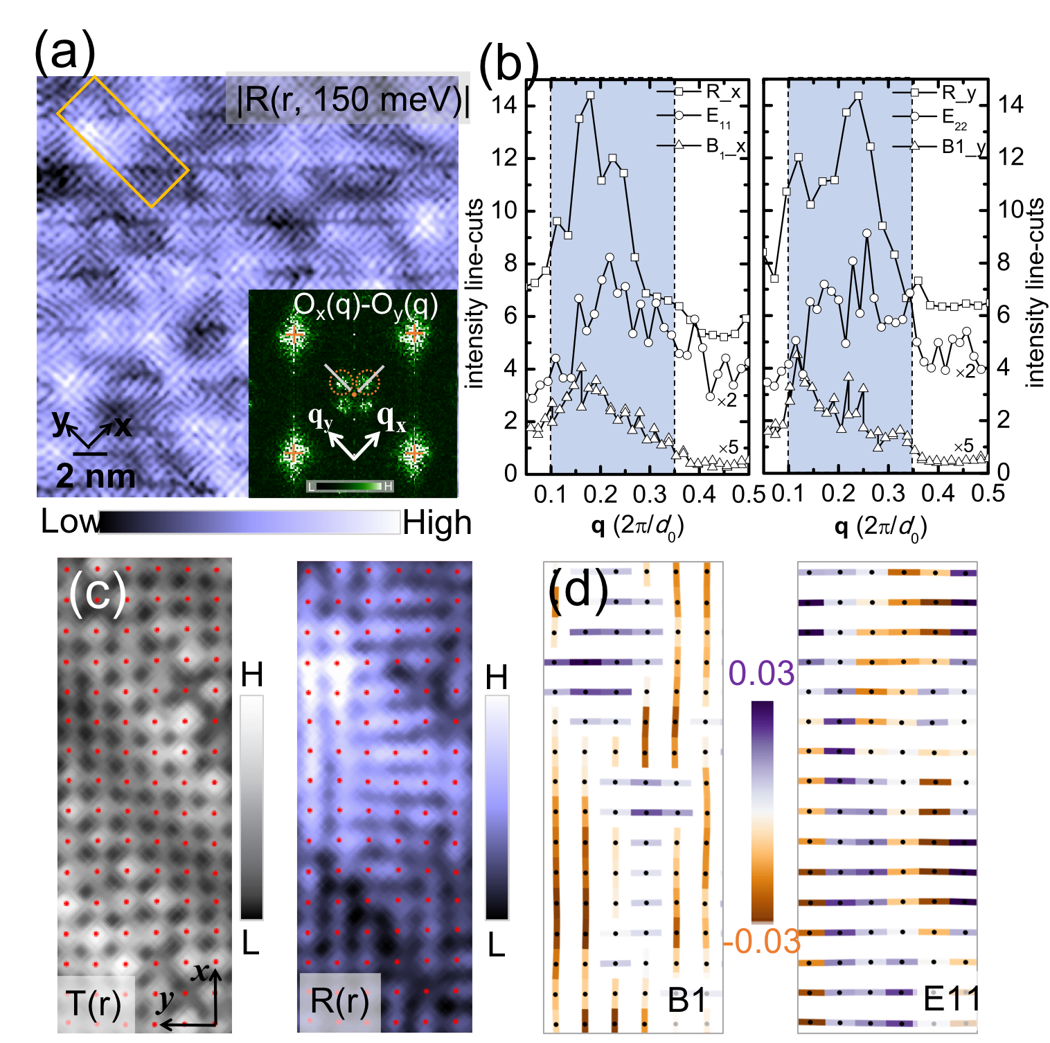
In Fig. 4(a), we show (r,150mV), the ratio of the tunneling current measured at opposite bias voltages, which has been demonstrated to represent the cuprate dCDW without ambiguity, since the ratio can effectively mitigate a systematic error in the measurement related to the junction formation [30]. As shown in Fig.4(a), unidirectional density wave modulations along both and directions are clearly visualized, and the inset shows the phase-resolved sub-lattice Fourier transform in a -symmetry channel[10], clearly showing peaks near q(1/4,0);(0, 1/4). This confirms that the electronic degrees of freedom at the Ox and Oy sites are out of phase by , indicating that the short-range density wave holds d-symmetry even at . In Fig.4(b), we show a comparison of the line profiles from (q,150mV), (q),(q), and S(q) for both (left) and (right) directions, where they all show peaks near q. Note that peak positions of the line profiles for (q,150mV) and (q) are not peaked at exactly q; this is most likely due to the discommensuration of the CDW domains[27]. A precise estimation of the wavevectors for , and and a study of their amplitudes and phases in relationship to the electronic structure is an intriguing direction for the future studies.
IV Discussion
Figures 4(c) and (d) summarize the situation occurring in both the electronic and lattice structures within a canonical dCDW that is extracted from the black rectangle in Fig. 2. The CDW breaks both the rotational and the translational symmetry as shown in Fig. 4(c) (right) together with the simultaneous topography (left), in which local atomic displacements are clearly seen (red dots are the locations of atoms). Our observations indicate that the unidirectionality of the CDW couples to the lattice, in which the bond length is periodically stretched and shrunk as revealed in the representation (half-breathing mode) [Fig. 4(d) right], having a relatively shorter bond length at the bond center of the CDW [28]. Simultaneously, a modulated intra-unit-cell rotational symmetry breaking of a -symmetry electronic degree of freedom couples to the lattice, displacing the atoms as revealed in the representation (quadrupolar mode) [Fig.4(d) left].
From these results, one notices that the bond length modulations in the and (, ) representations show a strong correspondence to the electronic properties of the CDW seen in the pseudogap states. First, the CDW is highly unidirectional, breaking both rotational and translational symmetries[10,26]. Second, it is highly heterogeneous[26]. Third, it is predominantly -symmetry[10,26]. Fourth, the periodicity of the CDW modulation is close to four-unit cells[10,31]. Thus, the modulations in (q),(q),and (q) together with the strong correspondence to (r,150mV) indicate that there are significant electron-lattice interactions, reflecting the observation that the atoms are displaced in the same symmetrical fashion as those for the density wave in the electronic structure at the pseudogap energy scale. The presence of such coupling indicates that the modulations seen in (r,150mV) indeed carry a charge degree of freedom, that of a charge density wave with -symmetry (CDW), since an electron-lattice interaction requires a local charge density.
In addition, it is natural to speculate that the periodic lattice displacements visualized in representations would be linked to the phonon dynamics reported in recent resonant X-ray measurement[17], in which the interplay of the bond-stretching phonons and charge order fluctuations are increased with lowering temperature below . The wavevector at which the phonon anomalies occur is quite similar to the one observed in the representations, suggesting that the periodic lattice displacements in representations correspond to a locally-frozen version of the soft phonons and consistent with the lock-in mechanism of the CDW by the electron-phonon coupling [32] for our Bi2Sr2CaCu2O8+δsample. The lack of spatial homogeneity of the bond-length modulations, as shown in Fig. 1(b), can be linked to the quantum fluctuations of the density waves inside the superconducting dome that are associated with the corresponding quantum critical point located just beyond the optimal doping [17,33].
In this study, we have introduced a group theoretic symmetry decomposition algorithm to analyze the symmetry of a lattice as well as the local displacements of it in Bi2Sr2CaCu2O8+δ. First, we visualized the heterogeneity of the in-plane bond lengths, for which the fluctuation is about 2 of the unit-cell distance. Second, the bond lengths themselves are spatially modulating at four-unit-cell periodicity. Third, , , and representations of the bond length are modulating at similar periodicity. Fourth, a strong correspondence between the -symmetry CDW and the displacements of the atoms visualized in the , , and representations of the bond length provides a direct real-space observation of the electron-lattice interactions for the first time, indicating that the charge degree of freedom is indeed involved in the CDW. Finally, the STM bond-length analysis offers a new paradigm for simultaneous studies of both the local lattice and electronic structures in quantum materials.
Acknowledgements.
We thank P. D. Johnson, Jiahao Yan, J. C. Davis for discussions. Work at Brookhaven is supported by the Office of Basic Energy Sciences, Materials Sciences and Engineering Division, U.S. Department of Energy under Contract No. DE-SC0012704.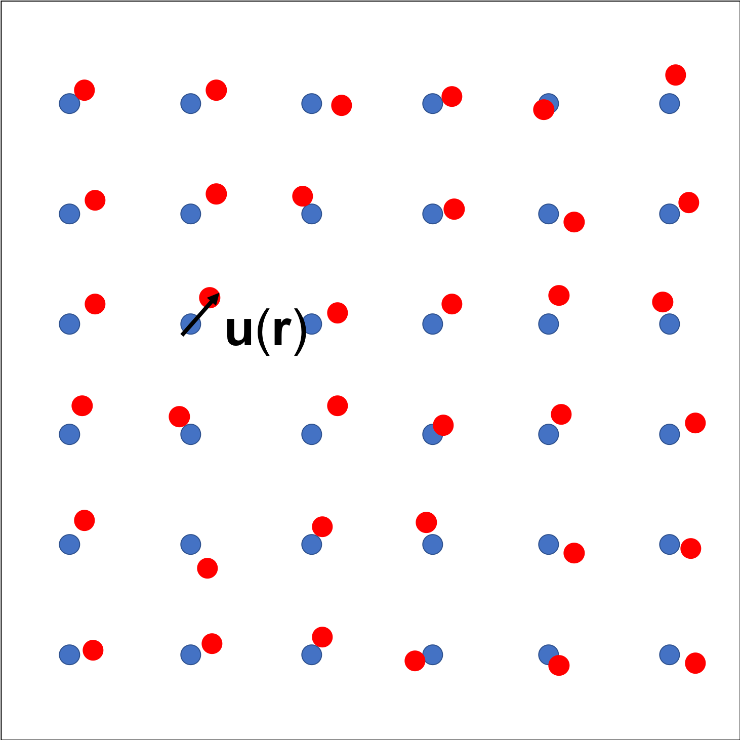
Appendix A Determination of the atomic sites
| Basic of the representation | Representation | Matrix represenation | |||||||
|---|---|---|---|---|---|---|---|---|---|
| 1 | 1 | 1 | 1 | 1 | 1 | 1 | 1 | ||
| 1 | 1 | 1 | 1 | -1 | -1 | -1 | -1 | ||
| ) | 1 | -1 | 1 | -1 | 1 | 1 | -1 | -1 | |
| 1 | -1 | 1 | -1 | -1 | -1 | 1 | 1 | ||
For the purpose of the symmetry decomposition analysis, first, we apply the Affin transformations to the (r) and the simultaneously taken electronic structure images, so that the Bragg wavevectors Q1 and Q2 satisfy and Q after the transformation. Second, we apply the Lawler-Fujita algorithm [10] to remove a STM tip drift in the data. In this algorithm, we obtain a displacement field u(r), which is associated with the STM tip drift, to render (r) to be perfectly lattice periodic. Finally, Bi positions are determined in the topography, in which the STM tip drift is removed, but local lattice distortions remain. We describe these procedures step-by-step in the followings.
An original (r), in which the STM tip drift is embedded, is given by
| (2) | |||
where is an amplitude of the complex field for the wavevector Q and u(r) is the displacement field that distorts the [30]. A drift-corrected topography, is then obtained by
| (3) |
Similarly, the same displacement field u(r) is also used to remove the STM-tip drift for simultaneously measured electronic structure images. The Lawler-Fujita algorithm utilizes a two-dimensional lock-in technique to obtain complex fields (r) for a periodic modulation at Q. Amplitude and spatial phase shift are then obtained by the following equations,
| (4) |
| (5) |
| (6) |
where a coarse graining length. In the case of a tetragonal lattice that is characterized by two orthogonal Bragg vectors, Q1 and Q1, u(r) is then simply related to the phase shift as for and , such that u(r) is obtained by
| (7) |
For the Bi2Sr2CaCu2O8+δin this study, we use =30 Å to calculate u(r) and the topography , in which the STM tip-drift is removed, is obtained by (3). Note that the STM tip-drift occurs at much longer length scale than 30 Å and this value is still much longer than the lattice constant of the Bi2Sr2CaCu2O8+δ. This means that, while extrinsic distortions in due to the STM tip-drift are removed by (3), intrinsic local lattice distortions still remain in . Then, we filtered out the supermodulations.
Next, in order to locate Bi atoms, r in , for which atomic positions are displaced from the perfect lattice configuration, we apply the Lawler-Fujita algorithm [10] once again to to get a displacement field u’(r) with =6 Å. Now, the shorter coarse graining length is used to capture atomic scale local lattice distortions, and u’(r) characterizes how much the atoms are displaced from the perfect lattice configuration, which is again obtained by (7). Note that the perfect lattice does not have any disorder, such that atomic corrugations are purely described by periodic functions without the phase disorder. Thus, a position of the Bi atoms in the distorted lattice is obtained by
| (8) |
where r a vector that represents the position of the Bi atoms in the perfect lattice. r is a set of vectors that are 2 modulo in the phases of the perfect lattice,
| (9) |
| (10) |
and then, r is obtained by solving (9) and (10),
| (11) |
Finally, by plugging (11) into (8), the Bi atom positions without extrinsic distortions due to the STM tip drift but with intrinsic local lattice distortions are obtained in (r).
Appendix B SI-STM Measurements
All the SI-STM measurements reported in this study were performed at 11K on the custom-designed SI-STM system at the OASIS complex in BNL. A single crystal of the nearly optimally doped Bi2Sr2CaCu2O8+δ(K, ) is cleaved by the Kapton tape at room temperature in the preparation chamber at the pressure lower than 3×10⁻¹⁰ Torr. Prior to perform SI-STM measurements on Bi2Sr2CaCu2O8+δ, the STM tip was characterized on the single crystal Au(111) surface, which is prepared by several cycles of Ar+ sputtering and annealing at 450∘C.
Appendix C group
There are eight symmetry operations {, , , , , , , } and five irreducible representations {, , , and } in the point group. As shown in the Table 1, a character table for the point group shows the corresponding matrix presentation for each irreducible representation[18]. The matrix representation describes how variables are transformed by the symmetry operations for each representation. Figure 7 shows examples of how to calculate for each representation.
Appendix D Setup condition dependence
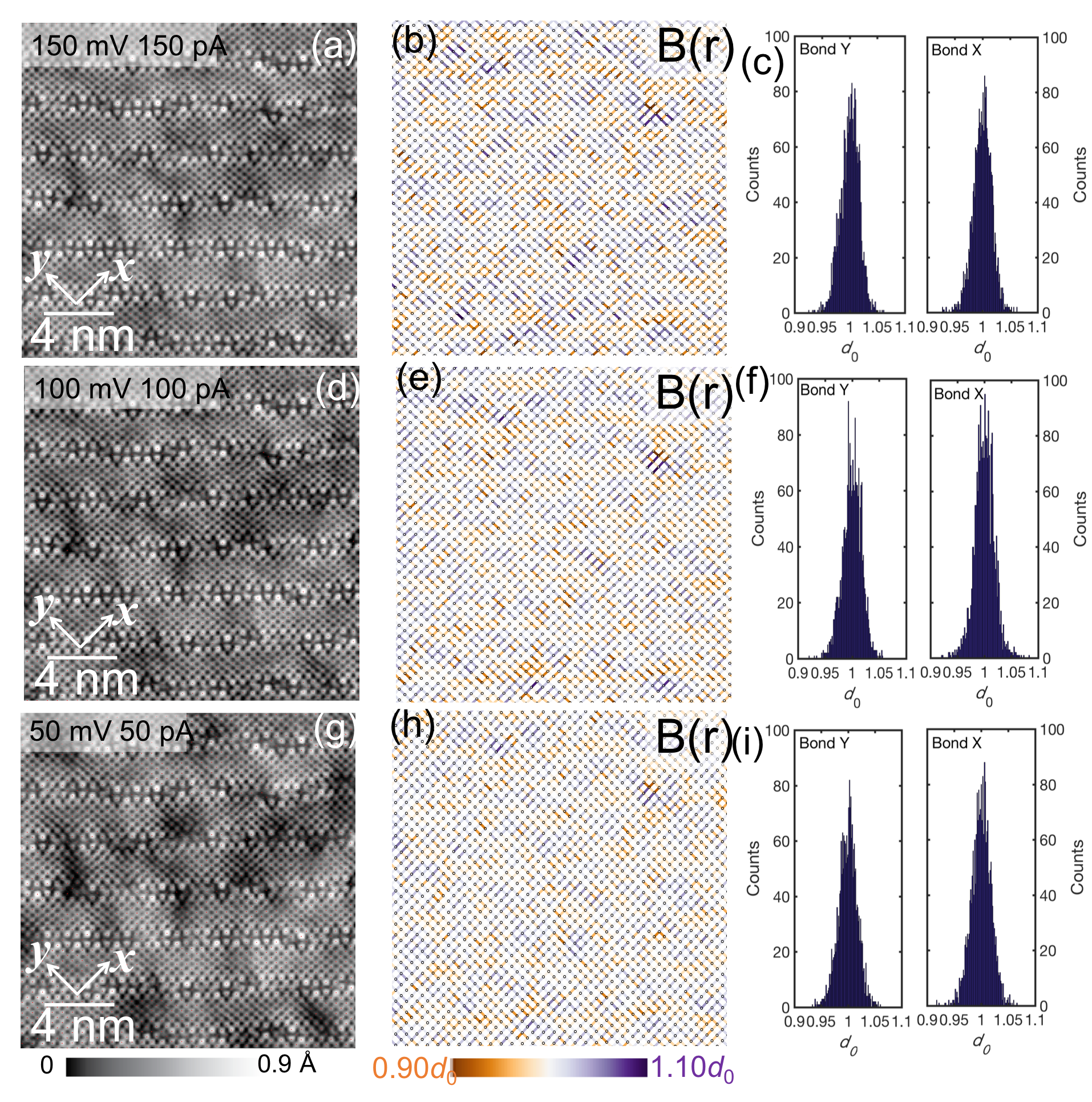
In order to verify that the bond map revealed in this study is not affected by the formation of the tunneling junction, which is set by the tunneling current, , and voltages, applied between the STM tip and sample, we have systematically measured topographies at different setup conditions in the same FOV [Figs. 10(a), (d), (g)]. At each setup conditions, bond maps are also calculated from the corresponding topographies measured. Figures 10(a), (d), (g) show topographies measured at (, ) = (150pA, 150 mV), (100pA, 100 mV) and (50pA, 50 mV), respectively (1GOhm junction resistance). The bond maps are extracted from Figs. 10(a), (d), and (g) and shown in Figs. 10(b), (e) and (h), respectively. Similarly, corresponding histograms of the bond lengths for both the and directions for each setup conditions are shown in Figs. 10(c), (f), and (i). The topographies, bond maps, and histograms measured at the different setup conditions virtually identical indicating that the setup effect is negligible within these conditions.
Appendix E Coarse graining length dependence
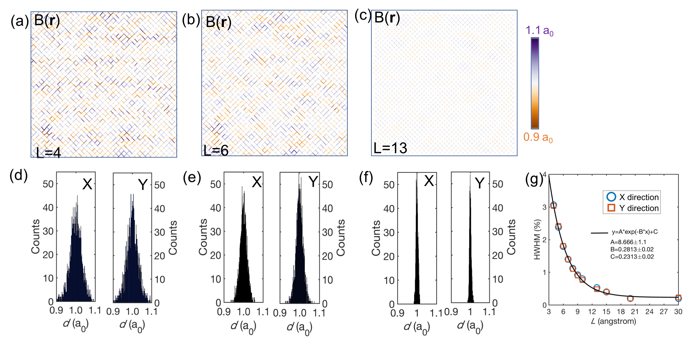
In this section, we show how the local fluctuation of the bond length changes with the size of the coarse graining length in eq.(4) and explain how we choose . Figs. 12 (a,b,c) show the bond length map obtained at 4, 6, 13 Å. With increasing , local lattice distortions are smoothed out and washed away when (Å), thus the local fluctuations of the bond length become undetectable. For an additional effect of the missing atoms that contributes to the bond length becomes obvious as weak horizontal contrasts since they are identified on top of the remnant supermodulations. Thus, 6 (Å) is the smallest size of the filter for precisely characterizing the local lattice distortion. Figs. 12 (d), (e) and (f) show distributions of the bond length for = 4, 6, 13 Å, respectively, from (a), (b) and (c), systematically showing a change in their height and width of the distribution. The half width at half maximum at each is plotted in Fig. 12 (g), indicating that for , the distribution becomes very sharp such that the large-scale fluctuations of the bond length are smoothed out and not detectable.
References
- Tsuei and Kirtley [2000] C. C. Tsuei and J. R. Kirtley, Pairing symmetry in cuprate superconductors, Rev. Mod. Phys. 72, 969 (2000).
- Comin and Damascelli [2016] R. Comin and A. Damascelli, Resonant x-ray scattering studies of charge order in cuprates, Annu. Rev. Condens. Matter Phys. 7, 369 (2016).
- Hinkov et al. [2008] V. Hinkov, D. Haug, B. Fauqué, P. Bourges, Y. Sidis, A. Ivanov, C. Bernhard, C. T. Lin, and B. Keimer, Electronic liquid crystal state in the high-temperature superconductor YBa2Cu3O6.45, Science 319, 597 (2008).
- Lawler et al. [2010] M. J. Lawler, K. Fujita, J. Lee, A. R. Schmidt, Y. Kohsaka, C. K. Kim, H. Eisaki, S. Uchida, J. C. Davis, J. P. Sethna, and E.-A. Kim, Intra-unit-cell electronic nematicity of the high-tc copper-oxide pseudogap states, Nature 466, 347 (2010).
- Ishida et al. [2020] K. Ishida, S. Hosoi, Y. Teramoto, T. Usui, Y. Mizukami, K. Itaka, Y. Matsuda, T. Watanabe, and T. Shibauchi, Divergent nematic susceptibility near the pseudogap critical point in a cuprate superconductor, J. Phys. Soc. Jpn 89, 064707 (2020).
- Agterberg et al. [2020] D. F. Agterberg, J. S. Davis, S. D. Edkins, E. Fradkin, D. J. V. Harlingen, S. A. Kivelson, P. A. Lee, L. Radzihovsky, J. M. Tranquada, , and Y. Wang, The physics of pair-density waves: Cuprate superconductors and beyond, Annu. Rev. Condens. Matter Phys. 11, 231 (2020).
- Du et al. [2021] Z. Du, H. Li, , and K. Fujita, Atomic-scale visualization of the cuprate pair density wave state, J. Phys. Soc. Jpn. 90, 111003 (2021).
- Blanco-Canosa et al. [2014] S. Blanco-Canosa, A. Frano, E. Schierle, J. Porras, T. Loew, M. Minola, M. Bluschke, E. Weschke, B. Keimer, , and M. L. Tacon, Resonant x-ray scattering study of charge-density wave correlations in YBa2Cu3O6+x, Phys. Rev. B 90, 054513 (2014).
- Chaix et al. [2017] L. Chaix, G. Ghiringhelli, Y. Y. Peng, M. Hashimoto, B. Moritz, K. Kummer, N. B. Brookes, Y. He, S. Chen, S. Ishida, Y. Yoshida, H. Eisaki, M. Salluzzo, L. Braicovich, Z.-X. Shen, T. P. Devereaux, and W.-S. Lee, Dispersive charge density wave excitations in Bi2Sr2CaCu2O8+δ, Nature Phys. 13, 952 (2017).
- Fujita et al. [2014a] K. Fujita, M. H. Hamidian, S. D. Edkins, C. . Kim, Y. Kohsaka, M. Azuma, M. Takano, H. Takagi, H. Eisaki, S. Uchida, A. Allais, M. J. Lawler, E. . Kim, S. Sachdev, and J. C. Davis, Direct phase-sensitive identification of a d-form factor density wave in underdoped cuprates, Proc. Natl’ Acad. Sci. 111, E3026 (2014a).
- Forgan et al. [2015] E. M. Forgan, E. Blackburn, A. Holmes, A. K. R. Briffa, J. Chang, L. Bouchenoire, S. Brown, R. Liang, D. Bonn, W. Hardy, N. Christensen, M. Zimmermann, M. Hucker, and S. Hayden, The microscopic structure of charge density waves in underdoped YBa2Cu3O6.54 revealed by x-ray diffraction, Nature Commun. 6, 10064 (2015).
- Hücker et al. [2011] M. Hücker, M. v. Zimmermann, G. D. Gu, Z. J. Xu, J. S. Wen, G. Xu, H. J. Kang, A. Zheludev, , and J. M. Tranquada, Stripe order in superconducting La2-xBaxCu (0.095 x 0.155), Phys. Rev. B 83, 104506 (2011).
- Abbamonte et al. [2005] P. Abbamonte, A. Ryusydi, S. Smadici, G. D. Gu, G. A. Sawatzky, , and D. L. Feng, Spatially modulated ‘mottness’ in in La2-xBaxCu, Nature Phys. 1, 155 (2005).
- Achkar et al. [2013] A. J. Achkar, F. He, R. Sutarto, J. Geck, H. Zhang, Y.-J. Kim, , and D. G. Hawthorn, Resonant x-ray scattering measurements of a spatial modulation of the cu 3d and o 2p energies in stripe-ordered cuprate superconductors, Phys. Rev. Lett. 110, 017001 (2013).
- McQueeney et al. [1999] R. J. McQueeney, Y. Petrov, T. Egami, M. Yethiraj, G. Shirane, and Y. Endoh, Anomalous dispersion of lo phonons in La1.85Sr0.15CuO4 at low temperatures, Phys. Rev. Lett. 82, 628 (1999).
- Reznik et al. [2006] D. Reznik, L. Pintschovius, M. Ito, S. Iikubo, M. Sato, H. Goka, M. Fujita, K. Yamada, G. D. Gu, and J. M. Tranquada, Electron–phonon coupling reflecting dynamic charge inhomogeneity in copper oxide superconductors, Nature 440, 1170 (2006).
- Lee et al. [2021] W. S. Lee, K.-J. Zhou, M. Hepting, J. Li, A. Nag, A. C. Walters, M. Garcia-Fernandez, H. C. Robarts, M. Hashimoto, H. Lu, B. Nosarzewski, D. Song, H. Eisaki, Z. X. Shen, B. Moritz, J. Zaanen, and T. P. Devereaux, Spectroscopic fingerprint of charge order melting driven by quantum fluctuations in a cuprate, Nature Phys. 17, 53 (2021).
- Inui et al. [1996] T. Inui, Y. Tanabe, and Y. Onoderar, Group theory and its applications in physics (springer series in solid-state sciences and 78), Springer (1996).
- Zeljkovic et al. [2015] I. Zeljkovic, D. Walkup, B. A. Assaf, K. L. Scipioni, R. Sankar, F. Chou, and V. Madhavan, Strain engineering dirac surface states in heteroepitaxial topological crystalline insulator thin films, Nature Nanotech. 10, 849 (2015).
- Machida et al. [2016] T. Machida, Y. Kohsaka, K. Matsuoka, K. Iwaya, T. Hanaguri, and T. Tamegai, Bipartite electronic superstructures in the vortex core of Bi2Sr2CaCu2O8+δ, Nature Commun. 7, 11747 (2016).
- Wang et al. [2017] Z. Wang, D. Walkup, P. Derry, T. Scadi, M. Rak, S. Vig, A. Kogar, I. Zeljkovic, A. Husain, L. H. Santos, Y. Wang, A. Damascelli, Y. Maeno, P. Abbamonte, E. Fradkin, and V. Madhavan, Quasiparticle interference and strong electron–mode coupling in the quasi-one-dimensional bands of Sr2RuO4, Nature Phys. 13, 799 (2017).
- Kan and Moss [1992] X. B. Kan and S. C. Moss, Four-dimensional crystallographic analysis of the incommensurate modulation in a bi2sr2cacu2o8 single crystal, Acta Cryst. B 48, 122 (1992).
- Castellan et al. [2006] J. P. Castellan, B. D. Gaulin, H. A. Dabkowska, A. Nabialek, G. Gu, X. Liu, , and Z. Islam, Two- and three-dimensional incommensurate modulation in optimally-doped Bi2Sr2CaCu2O8+δ, Phys. Rev. B 73, 174505 (2006).
- Hamidian et al. [2012] M. H. Hamidian, I. A. Firmo, K. Fujita, S. Mukhopadhyay, J. W. Orenstein, H. Eisaki, S. Uchida, M. J. Lawler, E. A. Kim, and J. C. Davis, Picometer registration of zinc impurity states in Bi2Sr2CaCu2O8+δ for phase determination in intra-unit-cell fourier transform stm, New J. Phys. 14, 053017 (2012).
- Tranquada et al. [1996] J. M. Tranquada, J. D. Axe, N. Ichikawa, Y. Nakamura, S. Uchida, , and B. Nachumi, Neutron-scattering study of stripe-phase order of holes and spins in La1.48Nd0.4Sr0.12CuO4, Phys. Rev. B 54, 748 (1996).
- Hamidian et al. [2016] M. H. Hamidian, S. D. Edkins, C. K. Kim, J. C. Davis, A. P. Mackenzie, H. Eisaki, S. Uchida, M. J. Lawler, E.-A. Kim, S. Sachdev, , and K. Fujita, Atomic-scale electronic structure of the cuprate d-symmetry form factor density wave state, Nature Phys. 12, 150 (2016).
- Mesaros et al. [2016] A. Mesaros, K. Fujita, S. D. Edkins, M. H. Hamidian, H. Eisaki, S. i. Uchida, J. C. S. Davis, M. J. Lawler, , and E.-A. Kim, Commensurate 4a0-period charge density modulations throughout the Bi2Sr2CaCu2O8+δ pseudogap regime, Proc. Nat’l Acad. Sci. 113, 12661 (2016).
- Kohsaka et al. [2012] Y. Kohsaka, T. Hanaguri, M. Azuma, M. Takano, J. C. Davis, and H. Takagi, Visualization of the emergence of the pseudogap state and the evolution to superconductivity in a lightly hole-doped mott insulator, Nature Phys. 8, 534 (2012).
- Newns and Tsuei [2007] D. M. Newns and C. C. Tsuei, Fluctuating Cu–O–Cu bond model of high-temperature superconductivity, Nature Phys. 3, 184 (2007).
- Fujita et al. [2014b] K. Fujita, M. Hamidian, I. Firmo, S. Mukhopadhyay, C. K. Kim, H. Eisaki, S. Uchida, and J. Davis, Strongly correlated systems - experimental techniques, Springer (2014b).
- Comin et al. [2015] R. Comin, R. Sutarto, F. He, E. H. da Silva Neto, L. Chauviere, A. Fraño, R. Liang, W. N. Hardy, D. A. Bonn, Y. Yoshida, H. Eisaki, A. J. Achkar, D. G. Hawthorn, B. Keimer, G. A. Sawatzky, and A. Damascelli, Symmetry of charge order in cuprates, Nature Mater. 14, 796 (2015).
- Wang et al. [2021] Q. Wang, K. von Arx, M. Horio, D. J. Mukkattukavil, J. Küspert, Y. Sassa, T. Schmitt, A. Nag, S. Pyon, T. Takayama, H. Takagi, M. Garcia-Fernandez, K.-J. Zhou, and J. Chang, Charge order lock-in by electron-phonon coupling in La1.675Eu0.2Sr0.125CuO4, Sci. Adv. 7, eabg7394 (2021).
- Fujita et al. [2014c] K. Fujita, C. K. Kim, I. Lee, J. Lee, M. H. Hamidian, I. A. Firmo, S.Mukhopadhyay, H. Eisaki, S. Uchida, M. J. Lawler, E.-A. Kim, and J. C. Davis, Simultaneous transitions in cuprate momentum-space topology and electronic symmetry breaking, Science 344, 612 (2014c).