[table]capposition=top
Excitonic and deep-level emission from N- and Al-polar homoepitaxial AlN grown by molecular beam epitaxy
Abstract
Using low-temperature cathodoluminescence spectroscopy, we study the properties of N- and Al-polar AlN layers grown by molecular beam epitaxy on bulk AlN{0001}. Compared to the bulk AlN substrate, layers of both polarities feature a suppression of deep level luminescence, a total absence of the prevalent donor with an exciton binding energy of 28 meV, and a much increased intensity of the emission from free excitons. The dominant donor in these layers is characterized by an associated exciton binding energy of 13 meV. The observation of excited exciton states up to the exciton continuum allows us to directly extract the free exciton binding energy of 57 meV.
Introduction
The ultra-wide gap semiconductor AlN was first synthesized over a century ago,[1] but it has only recently been recognized that the unique physical properties of AlN make it of great interest for applications in novel electronic and optoelectronic devices. Apart from its direct band gap of 6.095 eV corresponding to an emission wavelength of 203 nm, most noteworthy are its large piezoelectric coefficients (1.5 C/m2 or 5 pm/V),[2] its high breakdown-field ( MV/cm) [3, 4], and its high thermal conductivity ( W/mK) [5]. Moreover, AlN has an exciton binding energy exceeding twice the value of at room temperature,[6] which is notably higher than in any other III-V semiconductor with the exception of hBN.[7] These properties make AlN an attractive material for applications in high-power and millimeter-wave electronics[8, 9, 10] as well as deep-ultraviolet (UV-C) light emission and lasing[11, 12, 13, 14]. The large exciton binding energy in AlN is also of high interest for the study of the fundamental science of excitons and their condensation[15].
This potential of AlN lay dormant until very recently, when researchers succeeded to synthesize large AlN crystals of high structural perfection with low dislocation densities (– cm-2) utilizing either physical vapor transport (PVT)[16, 17, 18, 19] for bulk growth, or hydride vapor phase epitaxy (HVPE)[20] for fabricating thick free-standing layers. The availability of AlN substrates has enabled studies of the fundamental properties of AlN, particularly regarding its spontaneous emission, yielding insight into valence-band ordering, spin-orbit and crystal-field splitting, spin exchange interaction, exciton binding energies, and the detection of impurities and defects. These investigations have been performed by either photo- or cathodoluminescence spectroscopy on PVT-grown bulk crystals,[16, 17, 18, 19] HVPE-grown free-standing substrates,[20] or homoepitaxial AlN layers grown by metal-organic chemical vapor deposition [21, 22, 23, 24, 18, 25].
Numerous studies have focused on the excitonic near-bandedge emission of AlN, resolving transitions due to lowest-energy free excitons with symmetry (often called A-excitons)[26] and several bound exciton transitions [23, 27]. At higher excitation densities, bi-exciton emission (M-band), inelastic exciton-exciton scattering bands (P-bands), and electron-hole plasma recombination were observed [22, 17]. Spectra recorded over a wider spectral range revealed the presence of deep luminescence bands in the 2–4 eV range that frequently dominate over the near-bandedge emission in terms of integrated intensity. The actual origin of these ubiquitous deep luminescence bands is unknown, but is generally believed to be related to complexes of native defects, particularly Al vacancies, with impurities such as Si and O that form DX centers in AlN. However, also other native defects and the impurity C have been suspected to play an important role in the transitions giving rise to these deep bands.[6, 19, 16]
In general, the incorporation of impurities and the formation of native point defects is related in a complex way to the particular growth method and conditions. Surprisingly, there seem to be no detailed studies of the spontaneous emission of homoepitaxial AlN films grown by molecular beam epitaxy (MBE). Furthermore, the point defect incorporation and formation often strongly depends on the bonding configuration on the growth front, i. e., its crystallographic orientation, as reported, for example, for GaN.[28] To the best of our knowledge, all of the available studies on the excitonic emission of AlN have been performed on films grown along the Al-polar ([0001]), semi-polar, or non-polar ([100] and [110]) directions. However, N-polar ([000]) (In,Ga)N/(Al,Ga)N heterostructures are of particular interest because they exhibit internal electrostatic fields opposite to those of their metal-polar counterparts, which is considered favorable for various advanced device concepts.[29, *akyol_Jpn.J.Appl.Phys._2011, *dong_Appl.Phys.Lett._2012, *han_Jpn.J.Appl.Phys._2012, *wong_Semicond.Sci.Technol._2013, *feng_J.Appl.Phys._2015, *vandeurzenlenEnhancedEfficiencyBottom2021, *choBlueGaLightemitting2019, *bharadwajEnhancedInjectionEfficiency2020, *leeLightemittingDiodesAlN2020, *bharadwajBottomTunnelJunction2020]
In the present work, we use cathodoluminescence (CL) spectroscopy in a scanning electron microscope (SEM) to analyze and compare N- and Al-polar homoepitaxial strain-free AlN films grown by MBE in terms of their near-bandedge (around 6 eV) and deep-level (2–4 eV) light emission. With respect to the bare substrate, we find that both N-polar and Al-polar films feature a suppression of deep-level luminescence, and the total absence of the donor dominating the NBE of the substrate. Furthermore, the intense free exciton emission in the films under investigation allows us to directly measure an exciton binding energy of 57 meV from the transition.
Experiments
The three samples under investigation were grown in an MBE system equipped with a radio-frequency plasma source for generating active N and solid-source effusion cells for Al. As substrates, we used bulk AlN wafers grown by PVT with a dislocation density cm-2. The layers were grown at substrate temperatures above 1000 ∘C under Al-stable conditions. Details on the surface preparation and growth parameters for the MBE growth of Al- and N-polar homoepitaxial AlN layers are given in Refs. 40, 41, 42, 43. Samples I and II consist of a 700 nm-thick Al-polar and a 900 nm-thick N-polar layer, respectively. Sample III consists of a 1-m-thick N-polar AlN layer that was capped with 6.7 nm heteroepitaxial GaN. This GaN cap layer serves as a passivation layer for the AlN surface and also acts as a charge-spreading layer during electron beam excitation. As reference and for comparison with other studies, a freestanding AlN substrate was used.
[\capbeside\thisfloatsetupcapbesideposition=right,center,capbesidewidth=4cm]figure[\FBwidth]
The samples were investigated by scanning transmission electron microscopy (STEM) on an aberration-corrected ThermoFisher Spectra 300 CFEG operated at 300 keV to confirm their polarity. STEM samples were prepared using a ThermoFisher Helios G4 UX Focused Ion Beam system. Carbon and platinum protective layers were deposited and a final milling step at 5 keV was used to minimize ion-beam damage. Additionally, atomic force microscopy (AFM) was performed on an Asylum Cypher AFM microscope in tapping mode for sample areas of 2 × 2 µm2 and 20 × 20 µm2. Furthermore, the concentrations of O, C, and Si were measured by time-of-flight secondary ion mass spectrometry (ToF-SIMS) performed by Evans Analytical Group. Finally, triple-axis x-ray diffraction (XRD) scans across the symmetrical 002 wurtzite reflection were measured using a Panalytical Empyrean x-ray diffractometer equipped with a PIXcel3D detector and Xe proportional detector. The monochromator consists of a hybrid two-bounce Ge220 crystal utilizing Cu radiation.
To analyze and compare the optical properties of these samples, low-temperature emission spectra were recorded by CL spectroscopy in a Zeiss Ultra55 SEM equipped with a He-cryo-stage allowing sample temperatures down to 10 K and a Gatan MonoCL4 detection system. The spectrometer is operated with two gratings, one blazed at 300 nm with 2400 grooves/mm (Fig. 2) and the other blazed at 250 nm with 1200 grooves/mm (Fig. 3), resulting in a spectral resolution of approximately 0.0035 and 0.007 eV for a slit width of 0.1 mm, respectively. Note that the line widths of the near-bandedge transitions are limited by this spectral resolution. The monochromator was calibrated using a Hg(Ar) spectral calibration lamp. The error of this calibration amounts to Å because of the spectral separation between the highest energy line of the lamp and the AlN near-bandedge emission. The samples were aligned with respect to the detection setup such that mostly light propagating parallel to the -axis, , and electric field polarization () orthogonal to the -axis, , was collected. The light was detected monochromatically with a photomultipier tube (PMT) while stepping through the spectral range and the spectra were converted to energy scale by a Jacobian transformation, taking into account the refractive index dispersion of air [44]. For the CL measurements, all of the AlN samples were sputter coated with 3 nm of Ti to reduce charging effects in the SEM.
Results and Discussion
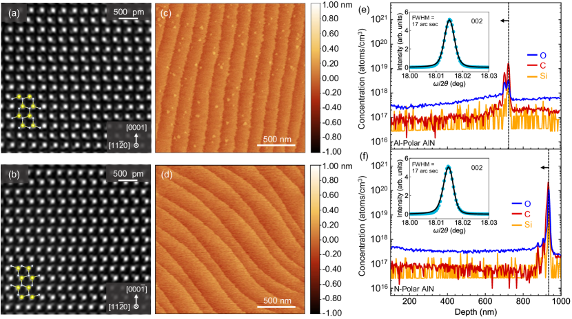
Figure 1 summarizes data pertaining to the structural and morphological properties of our AlN layers as well as to their purity. The polarity of the layers is examined by high-angle annular dark-field STEM (HAADF-STEM) as shown in Fig. 1(a) and 1(b), respectively. The yellow spheres in the overlayed ball-and-stick model of the wurtzite crystal structure represent Al atoms, and the white spheres represent N atoms, confirming the nominal polarity of the layers (growth direction pointing upwards). Figures 1(c) and 1(d) depict m2 atomic force topographs of the -plane surface of the as-grown layers. The trains of well-resolved monolayer steps are characteristic for step-flow growth, resulting in a root-mean-square roughness as low as 80 and 160 pm, respectively. Figures 1(e) and 1(f) display ToF-SIMS data for the respective samples revealing comparatively low impurity concentrations for layers of either polarity. The level of cm-3 is at, and the levels of O and C are close to the detection limit (given in parentheses): cm-3 ( cm-3) and cm-3 ( cm-3). Hydrogen (not shown) has a concentration below the detection limit for both samples, cm-3. Note that the spike at the substrate/MBE interface is less pronounced for the Al-polar sample (near 700 nm depth) than for the N-polar sample (near 900 nm depth). This is likely due to a greater adsorption efficiency of impurities on the N-polar surface [45, 46], as well as the less extensive ex-situ chemical treatment for the N-polar face, as it is more reactive [40, 42, 43]. Finally, the insets in Figs. 1(e) and 1(f) depict x-ray diffraction scans across the 002 reflection for the Al- and N-polar AlN samples (blue, dotted) compared with the bare AlN substrates they were grown on (solid, black). The line widths of approximately 17 arcsec confirm that the MBE-grown AlN layers are free of strain. The absence of strain is further confirmed by reciprocal space maps around the asymmetric reflection for Samples I and II (see Fig. S1 in the Supplementary Material). Symmetric and asymmetric scans recorded for Samples I and II exhibit widths between 20 and 30 arcsec, comparable or below to that measured on the corresponding bulk AlN substrates (see Fig. S2 in the Supplementary Material). For the structural characterization and SIMS data of sample III, we refer to Figs. S3, S4 and S5 in the Supplementary Material.
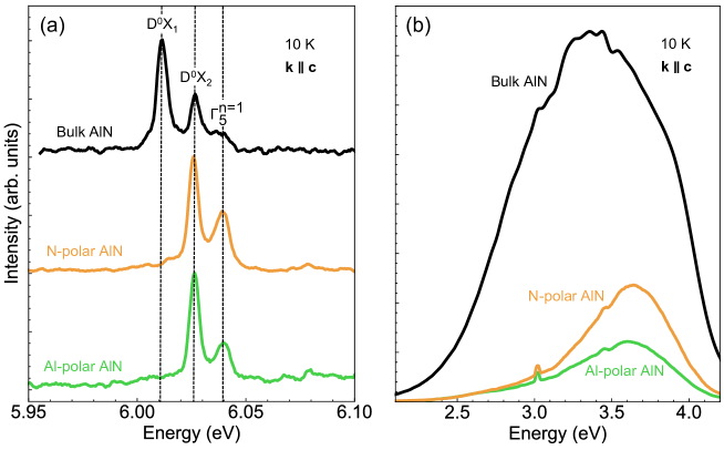
CL spectra of samples I and II are compared with the one of the bare PVT-AlN substrate (N-polar face) in Fig. 2. An acceleration voltage of 7 keV was used to excite the samples, ensuring that electron-hole pairs are generated only within the homoepitaxial layers (first few hundred nm from the AlN/air interface, see Fig. S7 in the Supplementary Material). Figure 2(a) shows the low-temperature, high-resolution near-bandedge emission spectra normalized to their peak intensities. For all three samples, a distinct high-energy line is observed at eV, with the error due to the uncertainty of the wavelength calibration. This transition energy is close to the average energy (6.041 eV) reported for the exciton spin triplet with symmetry in bulk (strain-free) AlN.[21, 17, 22, 25, 23, 27]
For AlN, the negative crystal-field splitting causes the band to be the uppermost valence band,[47] resulting in exciton states of symmetry (often called A-excitons).[48] Spin-exchange interaction splits these states into excitons with the irreducible representation , with the spin triplet being the only optically active state that satisfies and , i. e., our measurement geometry. It should be noted that there currently is no consensus in the literature on the assignment of the experimentally observed emission lines and thus the ordering of the and states. In fact, researchers have reported both negative[49, 22, 25, 17, 23] and positive[18, 20, 50, 51, 52] values for the spin-exchange splitting . A possible explanation of this apparent discrepancy is the fact that depends sensitively on strain.[53, 54, 26] For the case of GaN, Paskov et al. [26] calculated the dependence of the splitting (which is given by ) on biaxial strain, and observed that it changes sign for a biaxial compressive strain as small as . The scatter of lattice constants of bulk AlN amount to a variation of with respect to the strain-free value,[55] which, in analogy to GaN, may already be sufficient to result in a significant change of the spin-exchange splitting in AlN. An explicit calculation as done by Paskov et al. [26] for GaN is required to see if this hypothesis can account for the conflicting results in the literature.
The data in the present work, which are obtained on strain-free AlN, support a negative value of and thus a lower energy for the as compared to the exciton. The geometry () of the measurements depicted in Figs. 2 and 3 is compatible with the detection of the , but not the exciton. This fact is confirmed by a comparison to measurements taken on the cross-section of sample I (see Fig. S6 in the Supplementary Material). In the emission normal to the cross-section (), we observe a superposition of the and excitons as expected from the selection rules. The intense emission of the exciton is situated at 6.031 eV, in between the and lines. The additional peak observed at higher energy (6.08 eV) for the homoepitaxial layers is attributed to the first excited state of the free exciton as discussed in more detail for sample III.
For the PVT substrate, two intense and narrow lines are observed 28 and 13 meV below the free exciton ground state. The former of these lines is absent for both samples I and II. These lines have been frequently observed in previous work, and are attributed to donor-bound exciton transitions. , with an exciton binding energy of 28 meV, has been tentatively assigned to either O [23] or Si [27] as the shallow donor, while the with a binding energy of 13 meV has been speculated to be related to a native shallow donor.[23] The dominance of the line in the spectra of the substrate, and the total absence of this transition in our epitaxial layers, implies a significantly lower concentration of the responsible shallow donor in the layers compared to the substrate. Accordingly, it is unlikely that this line is related to O, the concentration of which is even slightly higher in the layers than in the substrate [cf. Figs. 1(e) and 1(f)]. Si, in contrast, is below the detection limit for all samples, and it is thus possible that the actual concentration in the layers is much below that in the substrate. Our experiments are thus consistent with Si being the donor related to the line, adding support of the assignments made in Refs. 27, 56, 20.
To probe radiative deep levels, we performed CL measurements with lower resolution in the range of 2–4.2 eV as shown in Fig. 2(b). All spectra in this figure are normalized to their respective near-bandedge peak intensities. The integrated intensity of the broad luminescence bands observed in this spectral range exceeds the near-bandedge intensity by a factor 2.5 for the bulk AlN substrate, but is lower by factors of 0.5 and 0.8 for samples I and II, respectively. Apart from the higher intensity, the CL band from the substrate is much broader and seems to consist of two individual contributions, with the one at higher energy matching the energy of the band in samples I and II. The lineshape of samples I and II are almost identical, suggesting that similar types of defects are incorporated for both polarities.
The overall similarity between the radiative properties of the Al- and N-polar AlN samples is remarkable. In contrast, studies on N-polar GaN layers, regardless of whether being grown by MBE or MOCVD, have shown that it is difficult to obtain layers with a purity and emission characteristics equivalent to their Ga-polar counterparts. A higher incorporation efficiency of impurities as well as a lower formation energy for N vacancies in N-polar GaN growth are discussed as possible reasons for this difference in material quality [57]. Consequently, N-rich growth seems to be a prerequisite to suppress the formation of N vacancies for GaN() [28]. For AlN, our data show that the situation is much more favorable, suggesting that we may use the alignment of the polarization fields as an additional degree of freedom for the design of AlN-based light-emitters. Note, however, that interface recombination may become important in group-III nitride heterostructures, and may strongly depend on their polarity.[58, 59, 60]
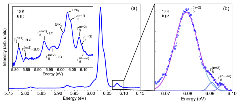
To further elucidate the details of the near-bandedge emission, we turn to sample III, which exhibits the highest emission intensity of all samples. Figure 3(a) shows its low-temperature CL spectrum, collected at an acceleration voltage of 11 keV (still exciting mostly the homoepitaxial layer, see Fig. S7 in the Supplementary Material). The higher beam energy ensures a high signal intensity, facilitating the reliable detection of weak transitions. As seen best in the inset, ten transitions are resolved, the energies of which are compiled in Table 1. The highest energy transitions associated to excited states of the free exciton are better visible in the magnified view displayed in Fig. 3(b). Where available, our values are in good agreement with previous studies. In particular, the exciton and its excited states are resolved at 6.038, 6.079, 6.091, and 6.095 eV, together with their longitudinal optical (LO) phonon replicas at lower energies. Again, the transition and a weak line (originating from the substrate) contribute to the spectra as well. The prominent transition at 6.079 eV can be readily assigned to the transition, for which energy separations of 37–43 meV with respect to the transition have been reported by other groups,[61, 17, 21, 18, 22, 23, 27] while no values are available for the higher-order transitions.
To identify the origin of the transitions at 6.091 and 6.095 eV, we first consider the hydrogenic effective-mass approximation, in which the energies of the excited states as well as the binding energy of the free exciton can be determined based on the 1S-2S splitting, i. e., the energy difference between the first excited state and the ground state . Specifically, the energy of the second excited state is predicted to be
| (1) |
Similarly, the energy of the transition is given by
| (2) |
These equations yield values of 6.087 and 6.093 eV for the and transitions, respectively, slightly lower than the transition energies observed.
| Transition | |||
|---|---|---|---|
| 5.815 | , [22] [20] | ||
| [22] | |||
| , [22] [20] | |||
| [22] | |||
| [25] | |||
| [25], [21], [27] | |||
| [25] | |||
| [17], [23], [27] | |||
| [25], [27] | |||
| [25], [27], [21] | |||
| [21], [27] | |||
| 6.031 | [25] | ||
| 0 | 0 | ||
| [25] | |||
| [21], [27], [25] | |||
The simple hydrogenic approximation is not expected to be in perfect agreement with the actual transition energies, since AlN exhibits a notable anisotropy regarding both the reduced exciton mass and the relative static permittivity . This anisotropy is commonly summarized in the form of the anisotropy parameter with the directions relative to that of the axis.[62, 63, 64, 65] For values of other than 1 or 0, exact analytical expressions for the excitonic levels do not exist. Gil et al.[64] have provided numerical values for the , , and transitions, placing them at 6.076, 6.083, and 6.086 eV for , the value obtained for AlN using the material parameters given in Ref. 65. These energies are systematically lower than those obtained by the simple hydrogen model because , which results in a reduction of the exciton binding energy. In fact, while the effective Rydberg energy amounts to 59 meV, where eV is the ionization energy of the hydrogen atom, the binding energy obtained within the framework of an anisotropic exciton is only 48 meV, as reported previously by Funato et al.[21] Even the experimentally observed 1S-2S splitting of 41 meV only allows for an exciton binding energy of 52 meV, still inconsistent with the highest energy feature observed in Fig. 3(b).
Indeed, for an accurate determination of the exciton binding energy in AlN, Ishii et al.[65] have pointed out that it is crucial to not only consider crystal anisotropy, but exchange and electron-phonon interactions as well. They showed the latter to result in a significantly increased exciton binding energy for the triplet, namely, 64 meV, accompanied by a 1S-2S splitting of 51 meV. Based on our transition energy of 6.038 eV, these values would result in transition energies for the and excitons of 6.089 and 6.102 eV, too large compared to the experimental values. Clearly, theory has still to be refined to accurately reproduce the excitonic transition energies observed experimentally. Currently, we share the observation in the literature that the hydrogenic approximation still seems to reproduce experimental data best.[49] Consequently, we assign the emission lines observed at 6.091 and 6.095 eV to the and states of the free exciton. The energy of the transition corresponds to the exciton continuum and thus the bandgap of AlN. Therefore, the energy difference between and directly provides the binding energy of the exciton, which thus amounts to 57 meV.
Other experimental values for the free exciton binding energy reported in the literature range from 47 to 67 meV. Those derived by relying on the 1S-2S spitting [61, 17, 21, 18, 22, 23, 27] or the energy difference between the free exciton transition and the exciton-exciton scattering band [17, 20] tend to be close to our value, with the average being about 54 meV. The large overall variation may be due to strain effects, sample heating (especially for high-excitation densities), and the large energy splitting between the and excitons [65].
Besides the zero-phonon exciton emission, we resolve two longitudinal optical (LO) phonon replicas each for the free exciton state and for the excited states from this sample. In Fig. 3(a), the LO phonon replicas are denoted as and with . The energy spacing between the phonon replicas and the main peaks is a multiple of 112 meV, in close agreement with the quantized LO phonon energy at the -point in AlN [66].
Table 1 summarizes all near-bandedge transition energies measured for our MBE films. Column lists the absolute transition energy, and column the energy shift with respect to the ground state exciton energy . Table 1 also gives values for of other transitions observed in studies in the literature but which are not observed in our films. Note that the actual origin of the , , , , and lines is not yet known. These lines are generally believed to originate from other donor-bound excitons because of their narrow linewidths, but the contribution of acceptor-bound excitons, inelastic scattering processes or many-body effects cannot be ruled out. [25, 21, 27] An extended table of all near-bandedge transitions that have been reported in literature can be found in the Supplementary Material (Table ST1).
Finally, it is interesting to discuss the lack of emission from the free exciton states in any previous study. At the first glance, it may appear surprising to see recombination from free carriers at a nominal temperature of 10 K, considering the strong Coulomb interaction in AlN. The fraction of excitons at a given temperature and electron-hole density is governed by Saha’s law[67] and is predicted to decrease with increasing carrier temperature and to increase with increasing electron-hole density below the Mott transition. In the majority of previous works, the samples were excited with an ArF laser, which delivers intense ns pulses with a low repetition rate and an energy close to the band edge. Due to the low repetition rate, the lowest excitation densities are typically around 50 kW/cm2, resulting in a carrier density on the order of cm-3. On the other hand, the excess energy delivered per pulse is comparatively low. For the present CL experiments, the situation is opposite. The continuous-wave excitation by the electron beam facilitates a comparatively low excitation density. In the present case, we estimate a carrier density of not more than cm-3 for an acceleration voltage of 11 kV, as detailed in the Supplementary Material.[68] The carrier temperature, however, is typically rather high, since the electron beam creates highly energetic secondary electrons and holes. The cooling of these hot carriers proceeds via the emission of LO phonons, thus creating a nonequilibrium population of hot LO phonons [69] that in turn heats the carrier distribution by strongly increasing the probability of LO phonon absorption. Indeed, from the high-energy slope of the transition,[67, 70] we deduce a carrier temperature of 120 K. With this carrier temperature and excitation density, Saha’s law (See figure S8 in the Supplementary Material) predicts an excitonic fraction of only 0.82, while for the carrier density estimated for ArF excitation, the fraction increases to 0.95 even for the same carrier temperature. These estimates provide a clear physical explanation for the prominence of excited exciton states in our CL experiments.
Conclusion
In summary and conclusion, we have investigated the properties of AlN layers grown by plasma-assisted MBE on both the N- and Al-polar faces of bulk AlN substrates. Regardless of polarity, the layers exhibit atomically smooth surfaces, high structural perfection and purity, and feature intense free exciton emission and suppressed emission from bound excitons and deep-level defects. These results highlight the potential of MBE for the growth of UV emitters. The ability to grow N-polar samples without compromising the crystal quality and thus to change the orientation of the polarization fields in AlN adds an additional degree of freedom that can be exploited in the design of MBE-grown deep-UV emitters. Finally, we have shown that the unique excitation conditions in CL spectroscopy facilitates the detection of several excited states of the exciton, including the excitonic continuum, directly yielding the exciton binding energy of 57 meV.
Supplementary Material
See the Supplementary Material for reciprocal space maps as well as symmetric and asymmetric scans of samples I and II, a detailed characterization of sample III (AFM, XRD, SIMS), CL spectra measured under different geometries (sample surface and cross-section), a discussion of the generation volume and excitation density in CL spectroscopy, the phase diagram of the coupled exciton-carrier system according to Saha’s law, as well as an extended table of the near-bandedge transitions observed in AlN.
Acknowledgements.
The authors thank Chandrashekhar Savant, Zexuan Zhang, and Shivali Agrawal for helpful discussions. This work was partially supported by the Cornell Center for Materials Research with funding from the NSF MRSEC program (Grant No. DMR-1719875). Further support was granted by the National Science Foundation with grant No. NNCI-2025233, DMR-1539918, RAISE-TAQS 1839196, MRI 1631282, and AFOSR Grant No. FA9550-20-1-0148. Finally, LvD acknowledges the "Deutscher Akademischer Austauschdienst" (DAAD) for funding provided through the Research Internships in Science and Engineering (RISE) Professional Scholarship.Author Declarations
Conflict of Interest
The authors have no conflicts to disclose.
Data Availability
The data that support the findings of this study are available within the article and its Supplementary Material. The raw data may be obtained from the corresponding author upon reasonable request.
References
- Briegleb and Geuther [1862] Fr. Briegleb and A. Geuther, “Ueber das Stickstoffmagnesium und die Affinitäten des Stickgases zu Metallen,” Justus Liebigs Ann. Chem. 123, 228–241 (1862).
- Muralt et al. [2009] P. Muralt, J. Conde, A. Artieda, F. Martin, and M. Cantoni, “Piezoelectric materials parameters for piezoelectric thin films in GHz applications,” Int. J. Microw. Wirel. Technol. 1, 19–27 (2009).
- Khachariya et al. [2022] D. Khachariya, S. Mita, P. Reddy, S. Dangi, J. H. Dycus, P. Bagheri, M. H. Breckenridge, R. Sengupta, S. Rathkanthiwar, R. Kirste, E. Kohn, Z. Sitar, R. Collazo, and S. Pavlidis, “Record 10 MV/cm mesa breakdown fields in Al0.85Ga0.15N/Al0.6Ga0.4N high electron mobility transistors on native AlN substrates,” Appl. Phys. Lett. 120, 172106 (2022).
- Hussain et al. [2023] K. Hussain, A. Mamun, R. Floyd, M. D. Alam, M. E. Liao, K. Huynh, Y. Wang, M. S. Goorsky, MVS. Chandrashekhar, G. Simin, and A. Khan, “High figure of merit extreme bandgap Al0.87Ga0.13N-Al0.64Ga0.36N heterostructures over bulk AlN substrates,” Appl. Phys. Express (2023), 10.35848/1882-0786/acb487.
- Cheng et al. [2020] Z. Cheng, Y. R. Koh, A. Mamun, J. Shi, T. Bai, K. Huynh, L. Yates, Z. Liu, R. Li, E. Lee, M. E. Liao, Y. Wang, H. M. Yu, M. Kushimoto, T. Luo, M. S. Goorsky, P. E. Hopkins, H. Amano, A. Khan, and S. Graham, “Experimental observation of high intrinsic thermal conductivity of AlN,” Phys. Rev. Mater. 4, 044602 (2020).
- Koppe, Hofsäss, and Vetter [2016] T. Koppe, H. Hofsäss, and U. Vetter, “Overview of band-edge and defect related luminescence in aluminum nitride,” J. Lumin. 178, 267–281 (2016).
- Doan et al. [2016] T. C. Doan, J. Li, J. Y. Lin, and H. X. Jiang, “Bandgap and exciton binding energies of hexagonal boron nitride probed by photocurrent excitation spectroscopy,” Appl. Phys. Lett. 109, 122101 (2016).
- Bader et al. [2020] S. J. Bader, H. Lee, R. Chaudhuri, S. Huang, A. Hickman, A. Molnar, H. G. Xing, D. Jena, H. W. Then, N. Chowdhury, and T. Palacios, “Prospects for Wide Bandgap and Ultrawide Bandgap CMOS Devices,” IEEE Trans. Electron Devices 67, 4010–4020 (2020).
- Hickman et al. [2021] A. Hickman, R. Chaudhuri, L. Li, K. Nomoto, S. J. Bader, J. C. M. Hwang, H. G. Xing, and D. Jena, “First RF Power Operation of AlN/GaN/AlN HEMTs With 3 A/mm and 3 W/mm at 10 GHz,” IEEE J. Electron Devices Soc. 9, 121–124 (2021).
- Kim et al. [2023] E. Kim, Z. Zhang, J. Encomendero, J. Singhal, K. Nomoto, A. Hickman, C. Wang, P. Fay, M. Toita, D. Jena, and H. G. Xing, “N-polar GaN/AlGaN/AlN high electron mobility transistors on single-crystal bulk AlN substrates,” Appl. Phys. Lett. 122, 092104 (2023).
- Amano et al. [2020] H. Amano, R. Collazo, C. D. Santi, S. Einfeldt, M. Funato, J. Glaab, S. Hagedorn, A. Hirano, H. Hirayama, R. Ishii, Y. Kashima, Y. Kawakami, R. Kirste, M. Kneissl, R. Martin, F. Mehnke, M. Meneghini, A. Ougazzaden, P. J. Parbrook, S. Rajan, P. Reddy, F. Römer, J. Ruschel, B. Sarkar, F. Scholz, L. J. Schowalter, P. Shields, Z. Sitar, L. Sulmoni, T. Wang, T. Wernicke, M. Weyers, B. Witzigmann, Y.-R. Wu, T. Wunderer, and Y. Zhang, “The 2020 UV emitter roadmap,” J. Phys. D: Appl. Phys. 53, 503001 (2020).
- Zhang et al. [2019] Z. Zhang, M. Kushimoto, T. Sakai, N. Sugiyama, L. J. Schowalter, C. Sasaoka, and H. Amano, “A 271.8 nm deep-ultraviolet laser diode for room temperature operation,” Appl. Phys. Express 12, 124003 (2019).
- Zhang et al. [2022a] Z. Zhang, M. Kushimoto, A. Yoshikawa, K. Aoto, C. Sasaoka, L. J. Schowalter, and H. Amano, “Key temperature-dependent characteristics of AlGaN-based UV-C laser diode and demonstration of room-temperature continuous-wave lasing,” Appl. Phys. Lett. 121, 222103 (2022a).
- van Deurzen et al. [2022] L. van Deurzen, R. Page, V. Protasenko, K. Nomoto, H. G. Xing, and D. Jena, “Optically pumped deep-UV multimode lasing in AlGaN double heterostructure grown by molecular beam homoepitaxy,” AIP Adv. 12, 035023 (2022).
- Ginzburg [1976] V. Ginzburg, Key problems of physics and astrophysics (Mir Publishers, Moscow, 1976).
- Zhou et al. [2020] Q. Zhou, Z. Zhang, H. Li, S. Golovynskyi, X. Tang, H. Wu, J. Wang, and B. Li, “Below bandgap photoluminescence of an AlN crystal: Co-existence of two different charging states of a defect center,” APL Mater. 8, 081107 (2020).
- Feneberg et al. [2010] M. Feneberg, R. A. R. Leute, B. Neuschl, K. Thonke, and M. Bickermann, “High-excitation and high-resolution photoluminescence spectra of bulk AlN,” Phys. Rev. B 82, 075208 (2010).
- Chichibu et al. [2013] S. F. Chichibu, K. Hazu, Y. Ishikawa, M. Tashiro, T. Ohtomo, K. Furusawa, A. Uedono, S. Mita, J. Xie, R. Collazo, and Z. Sitar, “Excitonic emission dynamics in homoepitaxial AlN films studied using polarized and spatio-time-resolved cathodoluminescence measurements,” Appl. Phys. Lett. 103, 142103 (2013).
- Thonke et al. [2017] K. Thonke, M. Lamprecht, R. Collazo, and Z. Sitar, “Optical signatures of silicon and oxygen related DX centers in AlN,” Phys. Status Solidi A 214, 1600749 (2017).
- Ishii et al. [2022] R. Ishii, T. Nagashima, R. Yamamoto, T. Hitomi, M. Funato, and Y. Kawakami, “Stimulated emission mechanism of aluminum nitride,” Phys. Rev. B 105, 205206 (2022).
- Funato et al. [2012] M. Funato, K. Matsuda, R. G. Banal, R. Ishii, and Y. Kawakami, “Homoepitaxy and Photoluminescence Properties of (0001) AlN,” Appl. Phys. Express 5, 082001 (2012).
- Leute et al. [2009] R. a. R. Leute, M. Feneberg, R. Sauer, K. Thonke, S. B. Thapa, F. Scholz, Y. Taniyasu, and M. Kasu, “Photoluminescence of highly excited AlN: Biexcitons and exciton-exciton scattering,” Appl. Phys. Lett. 95, 031903 (2009).
- Feneberg et al. [2011] M. Feneberg, B. Neuschl, K. Thonke, R. Collazo, A. Rice, Z. Sitar, R. Dalmau, J. Xie, S. Mita, and R. Goldhahn, “Sharp bound and free exciton lines from homoepitaxial AlN,” Phys. Rev. B 208, 1520–1522 (2011).
- Chichibu et al. [2010] S. F. Chichibu, T. Onuma, K. Hazu, and A. Uedono, “Major impacts of point defects and impurities on the carrier recombination dynamics in AlN,” Appl. Phys. Lett. 97, 201904 (2010).
- Bryan et al. [2014] Z. Bryan, I. Bryan, M. Bobea, L. Hussey, R. Kirste, Z. Sitar, and R. Collazo, “Exciton transitions and oxygen as a donor in m-plane AlN homoepitaxial films,” J. Appl. Phys. 115, 133503 (2014).
- Paskov et al. [2001] P. P. Paskov, T. Paskova, P. O. Holtz, and B. Monemar, “Spin-exchange splitting of excitons in GaN,” Phys. Rev. B 64, 115201 (2001).
- Neuschl et al. [2012] B. Neuschl, K. Thonke, M. Feneberg, S. Mita, J. Xie, R. Dalmau, R. Collazo, and Z. Sitar, “Optical identification of silicon as a shallow donor in MOVPE grown homoepitaxial AlN,” Phys. Status Solidi B 249, 511–515 (2012).
- Tatarczak et al. [2021] P. Tatarczak, H. Turski, K. P. Korona, E. Grzanka, C. Skierbiszewski, and A. Wysmołek, “Optical properties of N-polar GaN: The possible role of nitrogen vacancy-related defects,” Appl. Surf. Sci. 566, 150734 (2021).
- Li et al. [2011] Z. Q. Li, M. Lestradet, Y. G. Xiao, and S. Li, “Effects of polarization charge on the photovoltaic properties of InGaN solar cells: Effects of polarization charge on photovoltaic properties of InGaN solar cells,” Phys. Status Solidi (a) 208, 928–931 (2011).
- Akyol et al. [2011] F. Akyol, D. N. Nath, E. Gür, P. S. Park, and S. Rajan, “N-Polar III–Nitride Green (540 nm) Light Emitting Diode,” Jpn. J. Appl. Phys. 50, 052101 (2011).
- Dong et al. [2012] K. Dong, D. Chen, B. Liu, H. Lu, P. Chen, R. Zhang, and Y. Zheng, “Characteristics of polarization-doped N-face III-nitride light-emitting diodes,” Appl. Phys. Lett. 100, 073507 (2012).
- Han et al. [2012] S.-H. Han, D.-Y. Lee, J.-Y. Lim, J. W. Lee, D.-J. Kim, Y. S. Kim, S.-T. Kim, and S.-J. Park, “Effect of Internal Electric Field in Well Layer of InGaN/GaN Multiple Quantum Well Light-Emitting Diodes on Efficiency Droop,” Jpn. J. Appl. Phys. 51, 100201 (2012).
- Wong et al. [2013] M. H. Wong, S. Keller, N. Dasgupta, Sansaptak, D. J. Denninghoff, S. Kolluri, D. F. Brown, J. Lu, N. A. Fichtenbaum, E. Ahmadi, U. Singisetti, A. Chini, S. Rajan, S. P. DenBaars, J. S. Speck, and U. K. Mishra, “N-polar GaN epitaxy and high electron mobility transistors,” Semicond. Sci. Technol. 28, 074009 (2013).
- Feng et al. [2015] S.-W. Feng, P.-H. Liao, B. Leung, J. Han, F.-W. Yang, and H.-C. Wang, “Efficient carrier relaxation and fast carrier recombination of N-polar InGaN/GaN light emitting diodes,” J. Appl. Phys. 118, 043104 (2015).
- van Deurzen et al. [2021] L. van Deurzen, S. Bharadwaj, K. Lee, V. Protasenko, H. Turski, H. G. Xing, and D. Jena, “Enhanced efficiency in bottom tunnel junction InGaN blue LEDs,” in Light-Emitting Devices, Materials, and Applications XXV, Vol. 11706 (SPIE, 2021) pp. 30–35.
- Cho et al. [2019] Y. Cho, S. Bharadwaj, Z. Hu, K. Nomoto, U. Jahn, H. G. Xing, and D. Jena, “Blue (In,Ga)N light-emitting diodes with buried n+–p+ tunnel junctions by plasma-assisted molecular beam epitaxy,” Jpn. J. Appl. Phys. 58, 060914 (2019).
- Bharadwaj et al. [2020a] S. Bharadwaj, J. Miller, K. Lee, J. Lederman, M. Siekacz, H. G. Xing, D. Jena, C. Skierbiszewski, and H. Turski, “Enhanced injection efficiency and light output in bottom tunnel-junction light-emitting diodes,” Opt. Express 28, 4489–4500 (2020a).
- Lee et al. [2020a] K. Lee, S. Bharadwaj, Y.-T. Shao, L. van Deurzen, V. Protasenko, D. A. Muller, H. G. Xing, and D. Jena, “Light-emitting diodes with AlN polarization-induced buried tunnel junctions: A second look,” Appl. Phys. Lett. 117, 061104 (2020a).
- Bharadwaj et al. [2020b] S. Bharadwaj, K. Lee, K. Nomoto, A. Hickman, L. van Deurzen, V. Protasenko, H. G. Xing, and D. Jena, “Bottom tunnel junction blue light-emitting field-effect transistors,” Appl. Phys. Lett. 117, 031107 (2020b).
- Cho et al. [2020] Y. Cho, C. S. Chang, K. Lee, M. Gong, K. Nomoto, M. Toita, L. J. Schowalter, D. A. Muller, D. Jena, and H. G. Xing, “Molecular beam homoepitaxy on bulk AlN enabled by aluminum-assisted surface cleaning,” Appl. Phys. Lett. 116, 172106 (2020).
- Lee et al. [2020b] K. Lee, Y. Cho, L. J. Schowalter, M. Toita, H. G. Xing, and D. Jena, “Surface control and MBE growth diagram for homoepitaxy on single-crystal AlN substrates,” Appl. Phys. Lett. 116, 262102 (2020b).
- Singhal et al. [2022] J. Singhal, J. Encomendero, Y. Cho, L. van Deurzen, Z. Zhang, K. Nomoto, M. Toita, H. G. Xing, and D. Jena, “Molecular beam homoepitaxy of N-polar AlN on bulk AlN substrates,” AIP Adv. 12, 095314 (2022).
- Zhang et al. [2022b] Z. Zhang, Y. Hayashi, T. Tohei, A. Sakai, V. Protasenko, J. Singhal, H. Miyake, H. G. Xing, D. Jena, and Y. Cho, “Molecular beam homoepitaxy of N-polar AlN: Enabling role of aluminum-assisted surface cleaning,” Sci. Adv. 8, eabo6408 (2022b).
- [44] J. Lähnemann, J. F. Orri, E. Prestat, H. W. Ånes, D. Johnstone, and N. Tappy, “Lumispy v0.2.1,” 10.5281/zenodo.4640445.
- Ye et al. [2008] H. Ye, G. Chen, Y. Zhu, and S.-H. Wei, “Asymmetry of adsorption of oxygen at wurtzite AlN (0001) and surfaces: First-principles calculations,” Phys. Rev. B 77, 033302 (2008).
- Miao et al. [2010] M. S. Miao, P. G. Moses, J. R. Weber, A. Janotti, and C. G. V. de Walle, “Effects of surface reconstructions on oxygen adsorption at AlN polar surfaces,” Europhys. Lett. 89, 56004 (2010).
- Li et al. [2003] J. Li, K. B. Nam, M. L. Nakarmi, J. Y. Lin, H. X. Jiang, P. Carrier, and S.-H. Wei, “Band structure and fundamental optical transitions in wurtzite AlN,” Appl. Phys. Lett. 83, 5163–5165 (2003).
- Cho [1976] K. Cho, “Unified theory of symmetry-breaking effects on excitons in cubic and wurtzite structures,” Phys. Rev. B 14, 4463–4482 (1976).
- Feneberg et al. [2013] M. Feneberg, M. Fátima Romero, B. Neuschl, K. Thonke, M. Röppischer, C. Cobet, N. Esser, M. Bickermann, and R. Goldhahn, “Negative spin-exchange splitting in the exciton fine structure of AlN,” Appl. Phys. Lett. 102, 052112 (2013).
- Ishii, Funato, and Kawakami [2020] R. Ishii, M. Funato, and Y. Kawakami, “Long-range electron-hole exchange interaction in aluminum nitride,” Phys. Rev. B 102, 155202 (2020).
- Chichibu et al. [2019] S. F. Chichibu, K. Kojima, K. Hazu, Y. Ishikawa, K. Furusawa, S. Mita, R. Collazo, Z. Sitar, and A. Uedono, “In-plane optical polarization and dynamic properties of the near-band-edge emission of an m-plane freestanding AlN substrate and a homoepitaxial film,” Applied Physics Letters 115, 151903 (2019).
- Ishii, Funato, and Kawakami [2013] R. Ishii, M. Funato, and Y. Kawakami, “Huge electron-hole exchange interaction in aluminum nitride,” Phys. Rev. B 87, 161204 (2013).
- Koda and Langer [1968] T. Koda and D. W. Langer, “Splitting of Exciton Lines in Wurtzite-Type II-VI Crystals by Uniaxial Stress,” Phys. Rev. Lett. 20, 50–53 (1968).
- Akimoto and Hasegawa [1968] O. Akimoto and H. Hasegawa, “Strain-Induced Splitting and Polarization of Excitons Due to Exchange Interaction,” Phys. Rev. Lett. 20, 916–918 (1968).
- Nilsson, Janzén, and Kakanakova-Georgieva [2016] D. Nilsson, E. Janzén, and A. Kakanakova-Georgieva, “Lattice parameters of AlN bulk, homoepitaxial and heteroepitaxial material,” J. Phys. D: Appl. Phys. 49, 175108 (2016).
- Neuschl et al. [2013] B. Neuschl, K. Thonke, M. Feneberg, R. Goldhahn, T. Wunderer, Z. Yang, N. M. Johnson, J. Xie, S. Mita, A. Rice, R. Collazo, and Z. Sitar, “Direct determination of the silicon donor ionization energy in homoepitaxial AlN from photoluminescence two-electron transitions,” Appl. Phys. Lett. 103, 122105 (2013).
- Zywietz, Neugebauer, and Scheffler [1999] T. K. Zywietz, J. Neugebauer, and M. Scheffler, “The adsorption of oxygen at GaN surfaces,” Appl. Phys. Lett. 74, 1695–1697 (1999).
- Fernández-Garrido et al. [2016] S. Fernández-Garrido, J. Lähnemann, C. Hauswald, M. Korytov, M. Albrecht, C. Chèze, C. Skierbiszewski, and O. Brandt, “Comparison of the luminous efficiencies of Ga- and N-polar InxGa1-xN/InyGa1-yN quantum wells grown by plasma-assisted molecular beam epitaxy,” Phys. Rev. Applied 6, 034017 (2016).
- Chèze et al. [2018] C. Chèze, F. Feix, J. Lähnemann, T. Flissikowski, M. Kryśko, P. Wolny, H. Turski, C. Skierbiszewski, and O. Brandt, “Luminescent N-polar (In,Ga)N/GaN quantum wells achieved by plasma-assisted molecular beam epitaxy at temperatures exceeding 700 °C,” Appl. Phys. Lett. 112, 022102 (2018).
- Auzelle et al. [2022] T. Auzelle, C. Sinito, J. Lähnemann, G. Gao, T. Flissikowski, A. Trampert, S. Fernández-Garrido, and O. Brandt, “Interface Recombination in Ga- and N-Polar GaN/(Al,Ga)N Quantum Wells Grown by Molecular Beam Epitaxy,” Phys. Rev. Applied 17, 044030 (2022).
- Murotani et al. [2009] H. Murotani, T. Kuronaka, Y. Yamada, T. Taguchi, N. Okada, and H. Amano, “Temperature dependence of excitonic transitions in a-plane AlN epitaxial layers,” J. Appl. Phys. 105, 083533 (2009).
- Baldereschi and Diaz [1970] A. Baldereschi and M. G. Diaz, “Anisotropy of excitons in semiconductors,” Nuov. Cim. B 68, 217–229 (1970).
- Muljarov et al. [2000] E. A. Muljarov, A. L. Yablonskii, S. G. Tikhodeev, A. E. Bulatov, and J. L. Birman, “Hyperspherical theory of anisotropic exciton,” J. Math. Phys. 41, 6026–6041 (2000).
- Gil et al. [2012] B. Gil, D. Felbacq, B. Guizal, and G. Bouchitté, “Excitonic states and their wave functions in anisotropic materials: A computation using the finite-element method and its application to AlN,” Phys. Status Solidi B 249, 455–458 (2012).
- Ishii, Funato, and Kawakami [2014] R. Ishii, M. Funato, and Y. Kawakami, “Effects of strong electron–hole exchange and exciton–phonon interactions on the exciton binding energy of aluminum nitride,” Jpn. J. Appl. Phys. 53, 091001 (2014).
- Davydov et al. [1998] V. Yu. Davydov, Yu. E. Kitaev, I. N. Goncharuk, A. N. Smirnov, J. Graul, O. Semchinova, D. Uffmann, M. B. Smirnov, A. P. Mirgorodsky, and R. A. Evarestov, “Phonon dispersion and Raman scattering in hexagonal GaN and AlN,” Phys. Rev. B 58, 12899–12907 (1998).
- Bieker et al. [2015a] S. Bieker, T. Henn, T. Kiessling, W. Ossau, and L. W. Molenkamp, “Spatially resolved thermodynamics of the partially ionized exciton gas in GaAs,” Phys. Rev. Lett. 114, 227402 (2015a).
- Jahn et al. [2022] U. Jahn, V. M. Kaganer, K. K. Sabelfeld, A. E. Kireeva, J. Lähnemann, C. Pfüller, T. Flissikowski, C. Chèze, K. Biermann, R. Calarco, and O. Brandt, “Carrier Diffusion in GaN : A Cathodoluminescence Study. I. Temperature-Dependent Generation Volume,” Phys. Rev. Applied 17, 024017 (2022).
- Lugli et al. [1987] P. Lugli, C. Jacoboni, L. Reggiani, and P. Kocevar, “Monte Carlo algorithm for hot phonons in polar semiconductors,” Appl. Phys. Lett. 50, 1251–1253 (1987).
- Bieker et al. [2015b] S. Bieker, T. Kiessling, W. Ossau, and L. W. Molenkamp, “Correct determination of low-temperature free-exciton diffusion profiles in GaAs,” Phys. Rev. B 92, 121201(R) (2015b).