Supercurrent mediated by helical edge modes in bilayer graphene
Abstract
Bilayer graphene encapsulated in tungsten diselenide can host a weak topological phase with pairs of helical edge states. The electrical tunability of this phase makes it an ideal platform to investigate unique topological effects at zero magnetic field, such as topological superconductivity. Here we couple the helical edges of such a heterostructure to a superconductor. The inversion of the bulk gap accompanied by helical states near zero displacement field leads to the suppression of the critical current in a Josephson geometry. Using superconducting quantum interferometry we observe an even-odd effect in the Fraunhofer interference pattern within the inverted gap phase. We show theoretically that this effect is a direct consequence of the emergence of helical modes that connect the two edges of the sample. The absence of such an effect at high displacement field, as well as in bare bilayer graphene junctions, confirms this interpretation and demonstrates the topological nature of the inverted gap. Our results demonstrate the coupling of superconductivity to zero-field topological states in graphene.
Helical edge modes in two-dimensional (2D) systems are an important building block for many quantum technologies, such as dissipationless quantum spin transportmurakami_2003_dissipationless ; roth_2009_nonlocal ; brune_2012_spin , topological spintronicstokura_2019_magnetic ; he_2022_topological , and topological quantum computationprada_andreev_2020 . Electrons traveling along these modes cannot invert their propagation direction unless their spin is flipped. As a consequence, they cannot backscatter as long as time-reversal symmetry is preserved (e.g. even in the presence of arbitrary non-magnetic defects). Helical states are expected to appear at the edges of 2D topological insulatorsfu_superconducting_2008-2 ; Beenakker_fermion_2013 or in one-dimensional semiconductors with large spin-orbit coupling (SOC)prada_andreev_2020 . Interestingly, single-layer graphene was the first theoretically predicted quantum spin Hall insulator kane_quantum_2005 , whereby the intrinsic SOC gives rise to helical edge states. However, the strength of this Kane-Mele type SOC () is too small ( 40 eV) to realize a topological phase in practice.
With the advent of graphene-based van der Waals heterostructures with exceptional electronic properties, several alternative approaches have been explored to create helical edge modes. These modes are shown to exist in the quantum Hall regime of single-layer graphene at filling factor under the application of a large in-plane magnetic field young_tunable_2014-1 , or using a substrate with an exceptionally large dielectric constant veyrat_helical_2020-1 . Using a double-layer graphene heterostructure, helical transport was also observed by tuning each of the layers to sanchez-yamagishi_helical_2017 . While these experiments did not involve superconductivity, they have been complemented by theoretical proposals showing that coupling the helical modes to a superconductor should give rise to topological superconductivity san-jose_majorana_2015 ; Finocchiaro_2017_quantum . Unlike the experiments involving topological insulatorshart_induced_2014 ; pribiag_edge_2015 ; wiedenmann_4pi_2016 ; bocquillon_gapless_2017 , the main practical drawback of these proposals is the requirement of large magnetic fields, which is detrimental to any system involving superconductors.
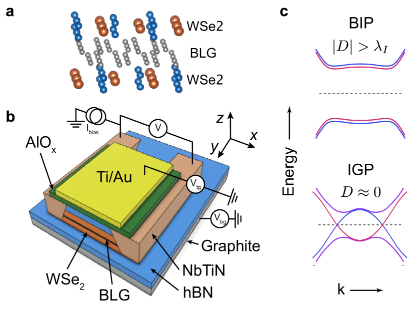
Recently, it was shown that helical modes can appear at zero magnetic field in bilayer graphene (BLG) encapsulated with , a transition metal dichalcogenide (TMD) island_spin-orbit_2019 . Several experiments have shown that graphene coupled to TMDs gives rise to a proximity induced Ising-type SOC, denoted wang_strong_2015-1 ; wang_origin_2016 ; wakamura_strong_2018 ; wakamura_spin-orbit_2019 ; zihlmann_large_2018 ; wang_quantum_2019 ; kedves_2023_stabilizing . In the case of BLG symmetrically encapsulated in (Fig. 1a), has opposite signs on the two graphene layers, thereby effectively emulating a Kane-Mele type SOC, but with a significantly larger magnitude of few meVszaletel_gate-tunable_2019 ; island_spin-orbit_2019 ; wang_quantum_2019 . Using an electric displacement field across the BLG, it was shown island_spin-orbit_2019 that the bandstructure could be tuned continuously from a band-insulator phase (BIP) at large , through a topological phase transition, and into an inverted-gap phase (IGP).
In this work we combine such a /BLG/ heterostructure with a superconductor and study the Josephson effect across this phase transition. We show that the IGP is characterized by a local minimum of the critical current . Supercurrents in this phase are expected to flow along the helical modes. We show theoretically that this should cause a unique even-odd modulation with flux in the Fraunhofer interference pattern of the Josephson junction (JJ), and present quantum interferometry measurements that clearly exhibit this signature. Importantly, the effect is absent in a trivial BLG system (i.e., without encapsulation) as well as in the BIP of /BLG/, thus ruling out trivial edge transport as its origin, and strongly supporting the topological nature of the superconducting IGP.
A schematic of the devices is shown in Fig. 1b (see Appendix A for details about the fabrication process). The /BLG/ heterostructure has superconducting NbTiN contacts as well as a back gate, , and a top gate, . We present results on two devices (Dev A and Dev B) fabricated on the same heterostructure. Dev A has a larger contact separation, 3.7 m, which suppresses the Josephson effect and allows us to study the normal state properties of the heterostructure. The supercurrent transport is explored in a ballistic JJ (Dev B) with a contact separation of 300 nm.
Figure 1c shows how the bandstructure is predicted to evolve as a function of displacement field . For the valence and conduction bands of the BLG are inverted due to the Ising SOC. The band inversion opens up a gap in the bulk band structure. Increasing introduces an additional competing energy . Here, nm is the BLG interlayer separation and is the out-of-plane dielectric constant of BLG. At large , becomes the dominant energy scale compared to and a gap associated with layer-polarised bands opens up. Thus, by tuning one can transition from the inverted phase (IGP: ) to band-insulator phase (BIP: ) via an inversion point, where the bulk gap closes.
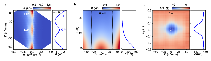
Before proceeding to the superconducting regime of our devices, we characterize the various phases in the normal regime. As a first step we measure the dependence of normal resistance with bottom and top gates, which independently control the carrier density, , and the displacement field, . The resistance as a function of and reveals a local maximum in close to along the line. This is consistent with the predicted opening of a SOC gap in the IGP (). A similar behavior has been observed previously in the form of an incompressible phase in capacitance measurements island_spin-orbit_2019 . As we increase , the gap is reduced and decreases, reaching a minimum at the gap-inversion point . Increasing further leads to an increase in as the band-insulator gap grows. The inversion points corresponding to minima are at and 35 mV/nm (Fig. 2a), which yield and meV.
The SOC gap can alternatively be probed by thermal excitation, see Fig. 2b. With increasing temperature, decreases as expected for a thermally activated gap. In addition, the local maximum at gradually becomes less pronounced as the temperature is increased, and completely vanishes at higher temperatures. To see this effect more clearly we determine the difference in the resistances at and at the inversion point mV/mm, i. e., . A positive value for implies the band inversion. This difference is almost zero at K (side panel of Fig. 2b), which corresponds to 2.2 meV. The estimated matches quite well with previously reported values of meV island_spin-orbit_2019 ; wang_quantum_2019 ; kedves_2023_stabilizing .
While the temperature dependence provides the information about the bulk gap, a verification of the existence and the helical character of edge states can be done by breaking time-reversal symmetry. An in-plane magnetic field introduces a Zeeman energy which opens a gap in the helical edge states island_spin-orbit_2019 , and removes their contribution from conduction. To check this effect we measure at in the presence of an in-plane magnetic field () as presented in Fig. 2c. At we observed a dip in magnetoresistance (0.3 T)](0.3 T) for 0.15 T indicating the extra conduction from edge states. At higher fields the absence of these gapless states results in values close to zero. Outside the IGP where no helical edge is present, for all . Additionally, we can rule out that this effect is related to the bulk bands as . Moreover, the positive for the complete field range is consistent with a band inversion originating from the SOC gap (side panel of Fig. 2c). At lower fields we once again see the presence of conducting edge channels resulting in a dip in .
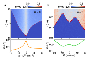
After verifying the presence of helical edge states, we turn our focus towards inducing superconductivity in these edge modes using JJs. The JJ (Dev B) is in the ballistic limit, as indicated by Fabry-Perot oscillations in the normal state transport Calado:NN15 ; Ben-Shalom:NP16 (see Appendix C). We first check the evolution of the critical current () in the JJ as a function of for fixed (Fig. 3a) and vice versa (Fig. 3b). The dependence of on is similar to several previous studies Heersche:N07 ; Calado:NN15 ; Ben-Shalom:NP16 ; allen_2016_spatially ; zhu_edge_2017 . Figure 3a shows an minimum at , coinciding with the maximum, while increases with higher electron/hole doping. The more interesting behavior is the dependence of at , displayed in Fig. 3b. We observe a local minimum in at , corresponding to the local maximum, and two maxima at higher values, concurrent to the minima at the gap inversion points. At higher , decreases monotonically due to gradual opening of band-insulator gap zhu_edge_2017 .
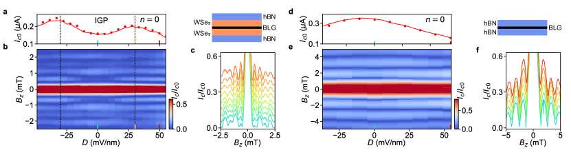
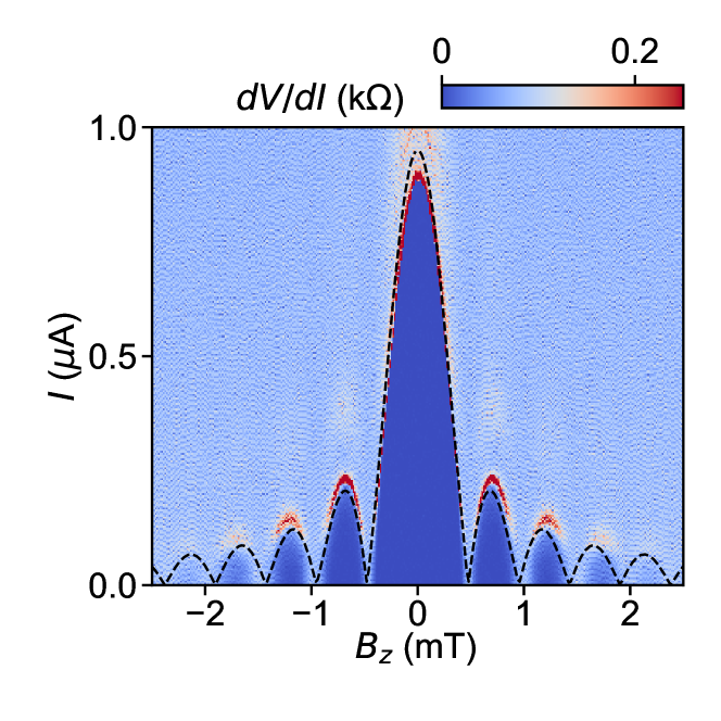
The presence of a supercurrent and its suppression at is a signature of Josephson coupling across a BLG in an inverted phase. However, it does not reveal whether the supercurrent flows through the bulk or through edge channels. One could attribute the suppression of in the IGP to the opening of a bulk SOI gap entirely. Therefore, demonstrating the existence of proximitized edge modes requires a different probe that can differentiate edge from bulk supercurrents. A common method employed for this purpose is superconducting quantum interferometry (SQI) hart_induced_2014 ; pribiag_edge_2015 ; allen_2016_spatially ; bocquillon_gapless_2017 ; zhu_edge_2017 ; de_vries_he_2018 ; de_vries_crossed_2019 , which involves the measurement of as a function of a perpendicular magnetic field . In the case of a JJ with homogeneous current transport across its width , should display a standard Fraunhofer pattern, following the functional form: , where and is the superconducting flux quantum. This regime is clearly observed in our samples at high densities , see Appendix E. On the other hand, for a JJ with only two superconducting and equivalent edges (i. e., a symmetric SQUID) one expects a SQI pattern of the form . However, the SQI pattern becomes more complicated if there is some coupling between these edges. An efficient inter-edge transport along edge channels flowing along the two SN interfaces (without becoming fully gapped by proximity) can lead to the electrons and holes flowing around the planar JJ, thereby picking up a phase from the magnetic flux. This phase introduces a -periodic component into the -periodic SQUID pattern of the edge supercurrent Baxevanis_even_2015 , which is a highly significant signature of the existence of proximitized helical modes.
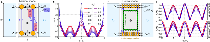
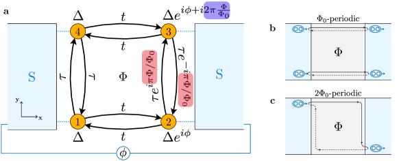
Given its importance for the interpretation of our SQI results, we now provide a theoretical analysis of how harmonics arise in as a result of electrons and holes circulating around the sample. We compute in a simple model containing the minimal ingredients to capture the effect (see the Appendix G for further details). The JJ with a gapped central region is abstracted into just four sites; one per corner of the BLG region. The parent superconductor induces on the -th corner a pairing potential , see Fig. 4a. The pairing phases depend on the magnetic flux through the BLG region, which is described by a gauge field . This makes the tight-binding Hamiltonian of the four sites strictly -periodic in . Next, we add two different hopping amplitudes between the corners, representing the existence of edge channels flowing around the central region. These hoppings acquire a Peierls phase induced by . The horizontal hoppings along the vacuum edges are denoted by . They have zero Peierls phase, and thus preserve the periodicity of the Hamiltonian. The vertical hopping along the left NS interface is denoted by , again with zero Peierls phase since it is located at . On the right NS interface at the hopping has the same modulus , but its Peierls phase is now , depending on the direction. This term makes the Hamiltonian -periodic when .
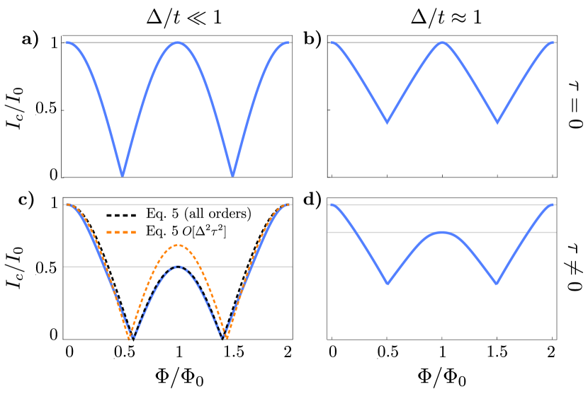
The critical current may be computed by maximizing the Josephson current versus , where is the free energy computed from . The resulting , shown in Fig. 4b, therefore inherits the periodicity of with . For a small and a small but finite , the resulting critical current is accurately approximated by Baxevanis_even_2015 for a positive that grows with , see the Appendices F and H. A finite results in an even-odd modulation of the SQUID-like pattern. As approaches , develops higher harmonics that deviate from this simple expression. The transport processes enabled by the coupling along the NS interfaces, i.e., by Josephson currents looping around the normal region, lead to the even-odd effect in the Fraunhofer pattern.
We now improve the minimal model by adopting a more microscopic description with several trivial transport channels flowing along vacuum edges allen_2016_spatially ; zhu_edge_2017 , and one helical mode flowing all around the BLG junction, as expected from the band-inverted phase zaletel_gate-tunable_2019 ; island_spin-orbit_2019 ; san-jose_majorana_2022 . A coupling between vacuum and helical states enables an inter-edge scattering mechanism, see Fig. 4c. This time the Peierls phase is incorporated into the tight-binding discretization of the different modes. Like in the minimal model, the inter-mode coupling and the superconducting proximity effect are both assumed to take place at the corners of the normal sample, whose bulk is again assumed to be completely gapped. Although these simplifying assumptions are not necessarily satisfied by the experimental samples, they are enough to confirm that the conclusions drawn from the minimal model still hold in a more generic situation, with propagating helical modes in place of a direct inter-edge hopping and with multiple trivial vacuum edge modes. The results for in the case of one and two vacuum edge modes are shown in Fig. 4(d,e). We once more find a -periodic SQUID-like pattern at (in red), representative of the non-inverted phase. By switching on the coupling , an even-odd modulation arises. This holds true also for higher number of vacuum modes. The main difference with respect to the minimal model is the behavior when , which is now less drastic.
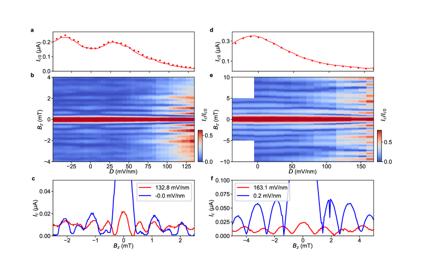
Keeping these theoretical results in mind, we measure the SQI patterns as a function of at (Fig. 5b,c). As predicted by our model, we observe an even-odd effect in the oscillations inside the IGP. Unlike in standard Fraunhofer and SQUID patterns, odd lobes are smaller than the adjacent even lobes, see for instance the lower curve of Fig. 5c. Such modulation is lost as we enter the BIP (upper curves), wherein an SQUID-like pattern is gradually recovered as is increased, probably originating from trivial and decoupled vacuum edge modes (see Appendix E). To confirm that the even-odd effect is associated to superconducting helical modes and not to bulk supercurrents, we perform control experiments on a bare hBN/BLG/hBN JJ (Dev C), where we expect no induced SOC and hence no helical modes. Indeed, we do not observe any even-odd effect in the control SQI patterns although the trivial edges are still present at higher (Fig. 5e,f and Appendix E).
Even-odd modulated SQI patterns have been experimentally reported in various 2D systems pribiag_edge_2015 ; bocquillon_gapless_2017 ; de_vries_he_2018 ; de_vries_crossed_2019 . In InAs- and InSb-based planar JJs de_vries_he_2018 ; de_vries_crossed_2019 , it was proposed that the effect stems from crossed Andreev reflection connecting the trivial edges of the JJs via conducting NS interfaces. Unfortunately, its origin was not fully clarified in the InAs and InSb experiments. In contrast, our symmetrically encapsulated BLG junctions offer a very natural candidate for an efficient inter-edge coupling mechanism, in the form of helical modes flowing along the two NS boundaries in the IGP. The even-odd effect then acquires a special significance in our experiment, as a direct probe of the weak-topological nature of the inverted gap, and as a demonstration of how can control the emergence of helical modes.
Our work provides the first experimental evidence of supercurrent flow along helical edges in graphene. The clear -periodic signature in our SQI experiment suggests an enticing prospect of detecting topological -periodic current-phase relations in this system Beenakker_fermion_2013 , which requires the investigation of the a.c. Josephson effect bocquillon_gapless_2017 ; wiedenmann_4pi_2016 ; Laroche_2019_observation and/or non-equilibrium effects at finite bias in a.c. supercurrent Haidekker_2020_superconducting . The observation of gate tunable helical-edge-mediated supercurrents opens a promising new avenue san-jose_majorana_2022 towards topological superconductivity and Majorana physics in van der Waals materials.
Data availability Raw data, analysis scripts and simulation code for all presented figures are available at Refs. prasanna_rout_2023_7944462, ; fernandopenaranda_2023_7941266, .
Author contributions P. R. and N. P. fabricated and measured the devices, and analysed the experimental data. S. G. conceived and coordinated the experiment. F. P., E. P. and P. S-J. developed the theoretical interpretation and models, and F. P. performed the simulations. All authors contributed to writing the manuscript.
Acknowledgements
We thank Joshua Island for discussions regarding heterostructure assembly and Tom Dvir for comments on the manuscript. This research was supported by an NWO Flagera grant and TKI grant of the Dutch Topsectoren Program, the Spanish Ministry of Economy and Competitiveness through Grants PCI2018-093026 (FlagERA Topograph) and PID2021-122769NB-I00 (AEI/FEDER, EU), and the Comunidad de Madrid through Grant S2018/NMT-4511 (NMAT2D-CM).
Appendix A Device fabrication
We exfoliate flakes of bilayer graphene (BLG), graphite (5-15 nm), tungsten diselenide WSe2 (10-35 nm) and hexagonal boron nitride hBN (20-55 nm) on different SiO2/Si substrates using Scotch tape. Then the stacks of hBN/WSe2/BLG/WSe2/hBN/graphite are assembled using the van der Waals dry-transfer using polycarbonate (PC) films on Polydimethylsiloxane (PDMS) hemispheres. The flakes are picked up at 110∘ C and the PC is melted at 180∘ C on SiO2/Si substrates in the end. After dissolving the melted PC in N-Methyl-2-pyrrolidone (NMP), the stacks are checked with atomic force microscopy (AFM).
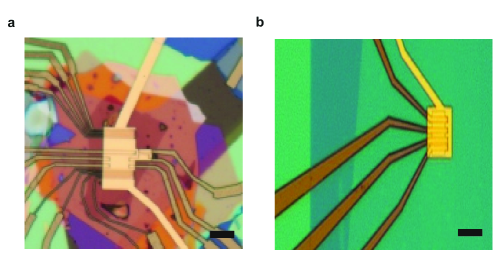
To fabricate the Josephson junctions (JJs) we spin coat a bilayer of 495 A4 and 950 A3 PMMA resists at 4000 rpm and bake at 175∘ C for 5 minutes, after each spinning. After the -beam lithography patterning, the resist development is carried out in a cold :IPA 3:1 mixture. We perform a reactive ion etching step using CHF3/ mixture (40/4 sccm) at 80 bar with a power of 60 W to etch precisely through the top hBN and WSe2. Then we deposit NbTi (5nm)/NbTiN (110 nm) by dc sputtering for superconducting edge contacts and lift-off in NMP at 80∘ C. In order to isolate the top gate metal from the ohmic, we deposit a 30 nm dielectric film of Al2O3 using atomic layer deposition (ALD) at 105∘ C. Finally we define the top gate by e-beam lithography, deposit Ti (5 nm)/Au (120 nm), followed by lift-off (Fig. S1).
In this work we measure three devices: two JJs with the hBN/WSe2/BLG/WSe2/hBN stack (Dev A, Dev B) and one JJ with hBN/BLG/hBN (Dev C). The two former JJs are 7 m wide and their respective lengths are 3.7 m (Dev A) and 300 nm (Dev B). Dev C is 3 m wide and 300 nm long.
Appendix B Measurements
All measurements are performed in a dilution refrigerator with a base temperature of 40 mK. Four-probe transport measurements are performed with a combination of DC and AC current bias scheme. To determine critical current we have employed a voltage switching detection method with current source and critical current measurement modules developed at TU Delft.ivvi The magnetic fields are applied by a 3D vector magnet, which enables us to align the field within 5∘ accuracy.
Appendix C /BLG/ devices
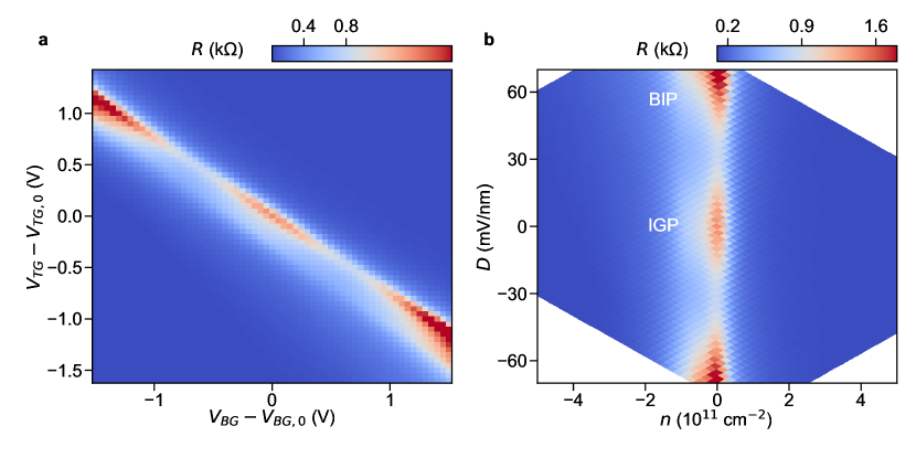
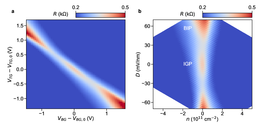
Figure S2a shows the dual gate (back gate and top gate ) map of the normal-state resistance for Dev A. In Fig. S2b, is replotted as a function of and . This clearly shows a resistance maximum near indicating the inverted-gap phase (IGP). Similar resistance maps are measured for Dev B (Fig. S3).
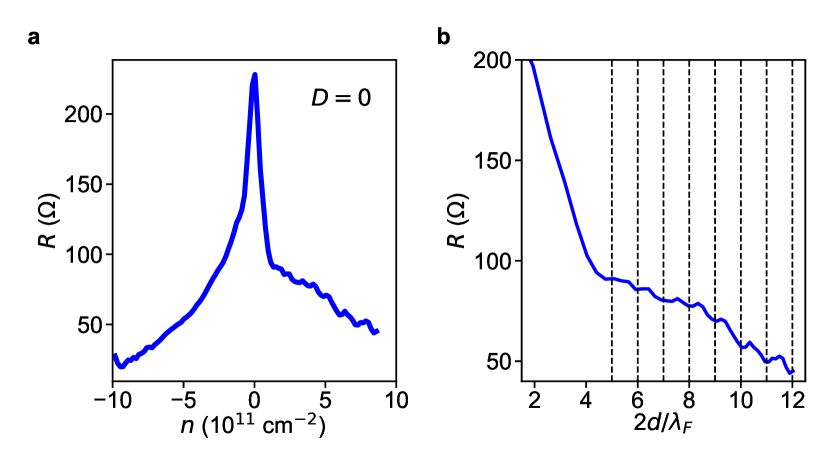
The existence of Fabry-Perot (FP) interferences in the normal-state resistance curve shows that Dev B is a ballistic JJ (Fig. S4). The FP resonances appear when the condition is satisfied, where is the cavity length, is an integer and is the Fermi wavelength. Figure S4b shows the resistance oscillations with a period of for nm.
Appendix D Bare BLG device
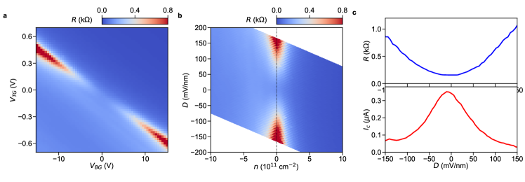
Figure S5 shows the resistance as a function of and (a) as well as a function of and (b) of the BLG JJ without any WSe2 encapsulation. Clearly we observe an increase in with increasing due to the opening of a trivial gap (Fig. S5c). In addition, the critical current gradually reduces with increasing as expected from the behaviour.
Appendix E SQI pattern at high doping
Figure S6 displays a Fraunhofer superconducting quantum interferometry (SQI) pattern for Dev B at cm-2 and . The SQI for a JJ with homogeneous supercurrent flow is of the form: , where is the zero-field critical current and is the (superconducting) flux quantum. The magnetic flux passing through the JJ is given by , where and are the length and width of the junction, respectively. However, the flux focusing increases the effective length. For our JJs the magnetic penetration depth of NbTiN ( 400 nm)Kroll_2019_magnetic is larger than the film thickness (110 nm) and the width of the electrode (300 nm). Thus, the effective JJ length is 600 nm. Using this value we plot the standard Fraunhofer curve in Fig. S6, which matches quite well the measured SQI pattern.
Appendix F SQI patterns for at larger
Figure S7 presents the SQI patterns measured at larger values and for Dev B and Dev C. As discussed in main text, the even-odd effect is only seen in the WSe2-encapsulated JJ. For large values we observe symmetric SQUID-like SQI patterns for both JJs indicating the presence of trivial edge states. These edge states have been previously observed in BLG JJs allen_2016_spatially ; zhu_edge_2017 .
Appendix G Formula for the critical current
Neglecting phase fluctuations, the critical current across a two-terminal JJ can be written as
| (1) |
where is the supercurrent at a given superconducting phase difference, , and magnetic flux, , threading the junction area. In the zero-temperature limit, can in turn be expressed purely as a function of spectral quantities, namely the system’s free energy , as
| (2) |
written as the sum of the energies over all occupied eigenstates of the junction Hamiltonian . These correspond to negative eigenvalues of the Bogoliubov-de Gennes (BdG) Hamiltonian.
Appendix H Construction of the four-site minimal model
In order to get physical insight into the processes that may give rise to an even-odd modulation in , we propose, prior to more elaborate calculations, the following minimal tight-binding model for the junction. It consists of only four sites located at the corners of the junction, see Fig. S8a. These four sites represent the normal region between the superconductors, and are threaded by a magnetic flux . Within this model, the sites labelled as and , and and are contacted to the left and right superconducting leads, respectively, in a JJ geometry. The resulting BdG Hamiltonian for a single spin species reads
| (3) |
written in the Nambu basis where and
| (4) | |||||
| (5) |
and are matrices corresponding to the normal Hamiltonian of the particle sector and the onsite superconducting electron-hole pairing terms induced by the leads, respectively. and are the induced pairing amplitude and phase from the parent superconductors, respectively. and are the hopping amplitudes between sites along the vacuum edge interfaces ( and ) and the NS interfaces ( and ), respectively. Thus, the ratio is a key quantity that controls the efficiency of the inter-edge coupling (between the top and bottom edges).
For the sake of simplicity, we assume that the system is spin degenerate and, thus, Eq. (3) can be regarded as half the BdG Hamiltonian of a spinful model. The previous assumption is justified as long as the magnetic length at is the largest spatial scale of the problem, which seems a good approximation for large-area devices.
The vector potential is chosen in the gauge , where and are the length and width of the junction, respectively. The origin of coordinates is chosen at site 1. The magnetic flux introduces a position-dependent modulation of the pairing phase, following , where is any given point inside the superconductor and the integral path is taken inside it. Taking in the left lead, adjacent to site 1, this introduces a phase at site 2 (junction phase difference picked along the outer loop between left and right) and at site . The latter makes the Hamiltonian -periodic in . In addition, enters as a Peierls phase in the hoppings. In the chosen gauge, the Peierls phase is non-zero only for hoppings connecting sites . The Peierls phase makes -periodic in , in contrast to the -periodicity from the pairing phases. From a different point of view, electrons and holes will pick up an Aharonov phase when circulating around the normal region (possible only if , which enables inter-edge scattering), which will produce a beating when added to the phase of a standard SQUID discussed in the main text. Thus, and despite its extreme simplicity, the four-site model allows us to identify inter-edge scattering as the key mechanism behind the even-odd effect.
Appendix I Regimes of the four-site model
Here we compute the critical current using Eqs. (1) and (2) and the spectrum of Eq. (3) in four different regimes. The results are shown in Fig. S9. The left and right columns correspond to the and regimes, respectively, whereas the top and bottom row contains the cases of forbidden or allowed inter-edge coupling controlled by . In the absence of inter-edge coupling, Fig. S9(a,b), the spectrum has -periodicity whose oscillations with may or may not touch zero at half-integer fluxes depending on the value of . A small ratio yields a complete suppression of at half-integer normalized flux (a) as opposed to (b).
The beating of the -periodic modulation comes from electron/hole trajectories encircling the sample [see Fig. 4(d, e)] and is enabled by a finite . In Fig. S9c, the experimentally relevant situation, the exact functional form, in blue, can be approximated by
| (6) |
depicted as a dashed black line, similar to Eq. (18) of Ref. Baxevanis_even_2015, obtained in the framework of a network (transfer-matrix) model. This approximation becomes exact, however, only in the limit of small and . In the general case, in contrast, the critical current receives contributions from all possible processes without spin mixing that lead to the net transfer of Cooper pairs across the junction and, therefore, involve an arbitrary number of loops around the sample and Andreev electron/hole conversions. To gain a better understanding of those that contribute to the -periodicity breaking, we focus on the leading processes up to order and corresponding to two Andreev reflections, one at each NS interface, and quasiparticle trajectories that encircles the device at most once, as those depicted in Fig. S8(b, c). In this limit, the critical currents at and read:
| (7) |
and
| (8) |
Substituting Eqs. (7) and (8) into Eq. (6) yields the dashed orange line in Fig. S9c that tends to the exact solution as . Despite its deviation from the calculations to all orders (blue and dashed black lines in Fig. S9) as we relax the condition, we conclude that loops of order and are the most relevant within the hierarchy of inter-edge processes that leads to -periodicity.
Appendix J Contribution to of processes
In this section we provide details of the derivation of Eqs. (7) and (8). We start by rewritting the BdG Hamiltonian of Eq. (3) into a normal and a superconducting part as:
| (9) |
In the regime of interest for the experiment, i.e., that of Fig. S9c with , can be regarded as a small perturbation to and, therefore, a perturbative treatment of the problem is justified. Let be the ’th eigensolution of
| (10) |
with energy . Since the unperturbed Hamiltonian does not couple the electron and hole sectors we can distinguish said eigenstates by their electron/hole character:
| (11) |
| (12) |
where and are the eigenstates of the Nambu projector , respectively, and () the eigenstates of (). They obey the so-called biorthonormality conditions, which in this basis reads:
| (13) |
and
| (14) |
Under standard perturbation theory the eigenstates and eigenvalues of can be expressed as:
| (15) |
| (16) |
where and corresponds to the ’th order contribution to the ’th eigenstate with corresponding energy of the perturbed problem, respectively.
Substituting the previous expansion into the Schrödinger equation for the full BdG Hamiltonian yields:
| (17) |
and
| (18) |
The artificial built-in redundancy of the Nambu representation for demands to use degenerate perturbation theory, as it reveals in the form of a two-fold degeneracy of the unperturbed energy levels, eventually splitted by the perturbation . Following Ref. Ling_perturbative_2021, we apply the following ansatz for the -th two-fold degenerate subspace of the unperturbed system:
| (19) |
where and are constants chosen to be real for simplicity. In a similar fashion, higher order eigenstates with can be decomposed as:
| (20) |
Note that the constraint in the sum together with Eq. (13) imposes that the first and subsequent perturbed eigenstates are orthogonal to , being consistent with the normalisation choice: .
The first and second energy corrections to can be readily found by substituting these ansatszes into Eq. (17) and Eq. (18), respectively, and solving the system of equations resulting from left multiplying it by . After some algebraic manipulations (see Ref. Ling_perturbative_2021, for instance) we get: , since the BdG Hamiltonian is hermitian. On the other hand, the second-order corrections are given by:
| (21) |
and similarly
| (22) |
with . Note that the bras and kets are the eigenstates of the normal Hamiltonian instead of those of the BdG in Eq. (9), a circumstance that greatly reduces the algebraic complexity.
Appendix K Construction of the multi-mode tight-binding model
Going beyond the four-site model, we consider the following tight-binding Hamiltonian
| (23) |
where comprises the Hamiltonians of three different regions [see sketch in Fig. 4c] and the couplings between them. The former reads
| (24) |
where , , and correspond, respectively, to the Hamiltonians of the IGP of BLG, two edge regions placed at the top and bottom interfaces to vacuum accounting for the expected formation of trivial edge channels, and the two s-wave superconducting leads at and with phase difference treated in mean-field. Setting the origin at the left bottom site of the NS interface, and using the same gauge for the vector potential as in the four-site model, the previous terms can be written as:
| (26) |
| (27) |
| (28) |
where creates at electron with spin at site , , , and are the chemical potentials at the helical, vacuum-edge, and superconducting regions, respectively, and where is the lattice constant and the electron mass. Note that in this Section denotes the parent superconducting pairing amplitude (instead of the induced one used in the four-site model and the main text). Channels in the vacuum-edge region are assumed to be decoupled from each other and ballistic. Finally, the helical region corresponding to the IGP only “sees” the superconductors through its coupling to the vacuum-edge region [see Fig. 4c], therefore the coupling Hamiltonian reads:
| (30) |
with
| (31) |
and
| (32) |
where and are the hopping amplitudes between sites at the IGP and thee vacuum edge and between the vacuum edge and the superconductor, respectively. Their magnitudes control the inter-edge coupling rate and transparency at the NS interfaces.
References
- (1) Murakami, S., Nagaosa, N. & Zhang, S.-C. Dissipationless quantum spin current at room temperature. Science 301, 1348–1351 (2003).
- (2) Roth, A. et al. Nonlocal transport in the quantum spin Hall state. Science 325, 294–297 (2009).
- (3) Brüne, C. et al. Spin polarization of the quantum spin Hall edge states. Nat. Phys. 8, 485–490 (2012).
- (4) Tokura, Y., Yasuda, K. & Tsukazaki, A. Magnetic topological insulators. Nat. Rev. Phys. 1, 126–143 (2019).
- (5) He, Q. L., Hughes, T. L., Armitage, N. P., Tokura, Y. & Wang, K. L. Topological spintronics and magnetoelectronics. Nat. Mater. 21, 15–23 (2022).
- (6) Prada, E. et al. From Andreev to Majorana bound states in hybrid superconductor-semiconductor nanowires. Nat. Rev. Phys. 2, 575–594 (2020).
- (7) Fu, L. & Kane, C. L. Superconducting proximity effect and majorana fermions at the surface of a topological insulator. Phys. Rev. Lett. 100, 096407 (2008). URL https://link.aps.org/doi/10.1103/PhysRevLett.100.096407.
- (8) Beenakker, C. W. J., Pikulin, D. I., Hyart, T., Schomerus, H. & Dahlhaus, J. P. Fermion-parity anomaly of the critical supercurrent in the quantum spin-Hall effect. Phys. Rev. Lett. 110, 017003 (2013). URL https://link.aps.org/doi/10.1103/PhysRevLett.110.017003.
- (9) Kane, C. L. & Mele, E. J. Quantum spin Hall effect in graphene. Phys. Rev. Lett. 95, 226801 (2005). URL https://link.aps.org/doi/10.1103/PhysRevLett.95.226801.
- (10) Young, A. et al. Tunable symmetry breaking and helical edge transport in a graphene quantum spin Hall state. Nature 505, 528–532 (2014).
- (11) Veyrat, L. et al. Helical quantum Hall phase in graphene on SrTiO3. Science 367, 781–786 (2020). URL https://www.science.org/doi/abs/10.1126/science.aax8201.
- (12) Sanchez-Yamagishi, J. D. et al. Helical edge states and fractional quantum Hall effect in a graphene electron–hole bilayer. Nat. Nanotechnol. 12, 118–122 (2017).
- (13) San-Jose, P., Lado, J. L., Aguado, R., Guinea, F. & Fernández-Rossier, J. Majorana zero modes in graphene. Phys. Rev. X 5, 041042 (2015). URL https://link.aps.org/doi/10.1103/PhysRevX.5.041042.
- (14) Finocchiaro, F., Guinea, F. & San-Jose, P. Quantum spin Hall effect in twisted bilayer graphene. 2D Materials 4, 025027 (2017).
- (15) Hart, S. et al. Induced superconductivity in the quantum spin Hall edge. Nat. Phys. 10, 638–643 (2014).
- (16) Pribiag, V. S. et al. Edge-mode superconductivity in a two-dimensional topological insulator. Nat. Nanotechnol. 10, 593–597 (2015).
- (17) Wiedenmann, J. et al. 4-periodic Josephson supercurrent in HgTe-based topological Josephson junctions. Nat. Commun. 7, 1–7 (2016).
- (18) Bocquillon, E. et al. Gapless Andreev bound states in the quantum spin Hall insulator HgTe. Nat. Nanotechnol. 12, 137–143 (2017).
- (19) Island, J. et al. Spin-orbit-driven band inversion in bilayer graphene by the van der Waals proximity effect. Nature 571, 85–89 (2019).
- (20) Wang, Z. et al. Strong interface-induced spin–orbit interaction in graphene on WS2. Nat. Commun. 6, 8339. URL https://www.nature.com/articles/ncomms9339.
- (21) Wang, Z. et al. Origin and magnitude of ’designer’ spin-orbit interaction in graphene on semiconducting transition metal dichalcogenides. Phys. Rev. X 6, 041020. URL https://link.aps.org/doi/10.1103/PhysRevX.6.041020.
- (22) Wakamura, T. et al. Strong anisotropic spin-orbit interaction induced in graphene by monolayer WS2. Phys. Rev. Lett. 120. URL http://arxiv.org/abs/1710.07483. eprint 1710.07483.
- (23) Wakamura, T. et al. Spin-orbit interaction induced in graphene by transition metal dichalcogenides. Phys. Rev. B 99, 245402. URL https://link.aps.org/doi/10.1103/PhysRevB.99.245402.
- (24) Zihlmann, S. et al. Large spin relaxation anisotropy and valley-Zeeman spin-orbit coupling in ${\mathrm{WSe}}_{2}$/graphene/$h$-BN heterostructures. Phys. Rev. B 97, 075434. URL https://link.aps.org/doi/10.1103/PhysRevB.97.075434.
- (25) Wang, D. et al. Quantum Hall effect measurement of spin–orbit coupling strengths in ultraclean bilayer graphene/WSe2 heterostructures. Nano Lett. 19, 7028–7034 (2019).
- (26) Kedves, M. et al. Stabilizing the inverted phase of a WSe2/BLG/WSe2 heterostructure via hydrostatic pressure (2023). eprint 2303.12622.
- (27) Zaletel, M. P. & Khoo, J. Y. The gate-tunable strong and fragile topology of multilayer-graphene on a transition metal dichalcogenide. arXiv:1901.01294 (2019).
- (28) Calado, V. E. et al. Ballistic josephson junctions in edge-contacted graphene. Nat Nano 10, 761–764 (2015).
- (29) Ben Shalom, M. et al. Quantum oscillations of the critical current and high-field superconducting proximity in ballistic graphene. Nature Physics 12, 318–322 (2016).
- (30) Heersche, H. B., Jarillo-Herrero, P., Oostinga, J. B., Vandersypen, L. M. K. & Morpurgo, A. F. Bipolar supercurrent in graphene. Nature 446, 56–59 (2007).
- (31) Allen, M. T. et al. Spatially resolved edge currents and guided-wave electronic states in graphene. Nat. Phys. 12, 128 (2016).
- (32) Zhu, M. et al. Edge currents shunt the insulating bulk in gapped graphene. Nat. Commun. 8, 1–6 (2017).
- (33) de Vries, F. K. et al. superconducting quantum interference through trivial edge states in inas. Phys. Rev. Lett. 120, 047702 (2018). URL https://link.aps.org/doi/10.1103/PhysRevLett.120.047702.
- (34) de Vries, F. K. et al. Crossed Andreev reflection in InSb flake Josephson junctions. Phys. Rev. Research 1, 032031 (2019). URL https://link.aps.org/doi/10.1103/PhysRevResearch.1.032031.
- (35) Baxevanis, B., Ostroukh, V. P. & Beenakker, C. W. J. Even-odd flux quanta effect in the Fraunhofer oscillations of an edge-channel Josephson junction. Phys. Rev. B 91, 041409 (2015). URL https://link.aps.org/doi/10.1103/PhysRevB.91.041409.
- (36) Peñaranda, F., Aguado, R., Prada, E. & San-Jose, P. Majorana bound states in encapsulated bilayer graphene. SciPost Phys. 14, 075 (2023).
- (37) Laroche, D. et al. Observation of the 4-periodic Josephson effect in indium arsenide nanowires. Nat. Commun. 10, 1–7 (2019).
- (38) Haidekker Galambos, T., Hoffman, S., Recher, P., Klinovaja, J. & Loss, D. Superconducting quantum interference in edge state Josephson junctions. Phys. Rev. Lett. 125, 157701 (2020). URL https://link.aps.org/doi/10.1103/PhysRevLett.125.157701.
- (39) Rout, P. et al. Data repository for “Supercurrent mediated by helical edge modes in bilayer graphene” (2023). URL https://doi.org/10.5281/zenodo.7944462.
- (40) Rout, P. et al. Code repository for “Supercurrent mediated by helical edge modes in bilayer graphene” (2023). URL https://doi.org/10.5281/zenodo.7941266.
- (41) Ivvi rack. https://qtwork.tudelft.nl/~schouten/ivvi/index-ivvi.htm.
- (42) Kroll, J. et al. Magnetic-field-resilient superconducting coplanar-waveguide resonators for hybrid circuit quantum electrodynamics experiments. Phys. Rev. Appl. 11, 064053 (2019). URL https://link.aps.org/doi/10.1103/PhysRevApplied.11.064053.
- (43) Ling, H. Y. & Kain, B. Selection rule for topological amplifiers in bogoliubov–de gennes systems. Phys. Rev. A 104, 013305 (2021). URL https://link.aps.org/doi/10.1103/PhysRevA.104.013305.