A Bi-CMOS electronic-photonic integrated circuit quantum light detector
Abstract
Complimentary metal-oxide-semiconductor (CMOS) compatible quantum technology enables scalable integration with the classical readout and control electronics needed to build quantum computers. Homodyne detectors have applications across quantum technologies including quantum computers, and they comprise photonics and electronics. Here we report a quantum noise limited monolithic electronic-photonic integrated homodyne detector, with an overall footprint of , fabricated in a 250 nm lithography bi-polar CMOS process. By monolithic integration of the electronics and photonics, overall capacitance is suppressed—this is the main bottleneck to high bandwidth measurement of quantum light. We measure a 3 dB bandwidth of 19.8 GHz and a maximum shot noise clearance of 15 dB. This exceeds bandwidth limits of detectors with macroscopic electronic interconnects, including wirebonding and flip-chip bonding. This demonstrates CMOS electronic-photonic integration enhancing performance of quantum photonics.
Photonic integrated circuits (PIC) are a compelling approach to develop quantum technology [1, 2] and they underpin proposed architectures for optical quantum computing [3, 4]. CMOS compatible PIC platforms, such as silicon on insulator photonics [5, 6], offer paths to scaling up the manufacture of photonic devices for quantum technology in commercial foundries. This may prove critical in the construction of universal quantum computers, because the scale and performance required of components to build quantum computers is beyond anything yet constructed in information technologies [3].
Since initial experiments with silicon quantum photonic circuits [7, 8], CMOS compatibility for electronic-photonic integration has been a clear goal for quantum photonics. This is because it would enable integration at scale of components generating and utilising quantum states of light with the required high performance classical readout and control electronics. But to date, the development of foundry ePIC platforms [9, 6] has been driven by the performance demands of classical applications, with demonstrations including 56 GB/s direct detection receivers [10] and 128 Gb/s coherent receivers [11] for fibre optics telecommunciations, and coherent detector arrays with active pixel amplifiers for 3D imaging [12].
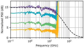
Here we demonstrate electronic-photonic integration can be applied to enhance quantum technologies. We report integration in one monolithic ePIC chip (Figure 1) of all the electronics and silicon photonics needed for homodyne detection of quantum optical signatures [13]. The detector has a measured 3-dB bandwidth of GHz and a maximum measured shot noise clearance of 15 dB. By extrapolating the measured clearance, we infer shot noise limited performance beyond the bandwidth of our analysis equipment, measuring more than 10 dB at 26.5 GHz.
Homodyne detectors can measure weak signals by interfering them with a local oscillator at an optical beamsplitter. The resulting interference is observed in the subtraction of photocurrents from a pair of photodiodes placed at the two beamsplitter outputs. This subtraction current requires amplification, and when the amplification electronics are of sufficiently low noise, the homodyne detector is sensitive enough to reveal quantum noise signatures in the input. This is quantified by the clearance between optical shot noise and the electronic noise of the detector. Quantum technology applications of homodyne detectors include squeezed-light-enhanced gravitational wave detection [14, 15], quantum state tomography [13], measuring continuous variables cluster states [16, 17] for quantum computing and for continuous variables quantum communication [18].
Waveguide integrated beamsplitters have been used for homodyne detection with silica-on-silicon [19] and lithium niobate PICs [20]. In silicon-on-insulator photonics, on-chip germanium p-i-n photodiodes have been integrated with waveguides and interfaced with discrete amplifier electronics for quantum random number generation and coherent state tomography [21], and as a chip-scale receiver for continuous variables quantum key distribution [22]. In these cases, the detector bandwidths were limited to respectively 100 MHz and 10 MHz by discrete electronics, mounted on printed circuit boards (PCB). Consequently, micro-electronic amplifiers were wirebonded to silicon PICs, and the resulting detectors demonstrated 3-dB bandwidths of 1.7 GHz [23] and 1.5 GHz [24] – these detectors were respectively used to measure squeezing over a 9 GHz bandwidth and observe shot noise clearance out to 20 GHz.
A remaining limiting factor in the speed of these detectors is the 20 fF - 100 fF capacitance overhead of the electrical bondpad interconnection [25], that interfaces the PIC with the integrated electronics. Flip-chip interfaces introduce similar capacitance overheads, and so also restrict the possible bandwidth of hybrid integration using macroscopic interconnects. In order to increase bandwidth further, monolithic integration is required.
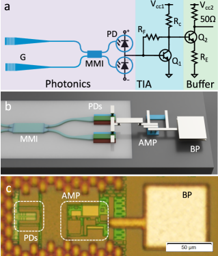
The reported single-chip homodyne detector is illustrated in Figure 1. It was designed and characterised in-house with fabrication outsourced to the Leibniz Institute for High Performance Microelectronics (IHP). We chose IHP’s SG25H5_EPIC process, which features a 250 m silicon node, germanium-based photodiodes with GHz and vertically integrated heterojunction bipolar transistors (HBTs) for RF applications using 250 nm lithography with a specified transition frequency GHz and a breakdown voltage of 1.7 V [9]. The RF performance of these HBTs is comparable to the lateral n-channel MOSFET transistors in references [26, 27, 28]. This is due to the vertical carrier transport of the HBT, meaning speed is less dependent on the lithography resolution allowing vertical bipolar transistors to outperform NMOS devices at the same process node [29]. The HBTs are integrated in the same front-end-of-line process as the silicon-on-insulator waveguides and active optical components, such as modulators and photodiodes. This approach removes all bondpad and packaging parasitics, with connections between photonics and electronics made in the metal interconnect layers of the back-end-of-line (BEOL).
The IHP fabrication process begins with a SOI wafer optimised for photonics, with a 220nm silicon layer thickness and a 2um thick buried oxide layer. A ‘local-SOI’ approach is employed in which SOI regions that are to be used for BiCMOS devices are etched down to the silicon substrate. Bulk silicon is selectively regrown epitaxially in these regions and is subsequently planarised using chemical-mechanical planarisation. Patterning of electronic and photonic structures is conducted in parallel and the electrical contacts to the photodiodes and transistors are made with the same process step [30]. Devices are then connected through a single shared BEOL with five metal layers.
The transimpedance amplifier (TIA) used consists of a HBT common-emitter amplifier in shunt-feedback configuration, followed by a 50 buffer amplifier for interfacing with standard radio frequency (RF) test equipment (see Figure 1). The bandwidth of a single-stage shunt-feedback TIA with an ideal second-order Butterworth response is given by [31]
| (1) |
where is the total capacitance at the amplifier input, is the feedback resistance and is the gain-bandwidth product. A monolithic design reduces by minimising the stray capacitance between the photodiodes and amplifier due to bondpads or other wiring related sources. This comes in addition to the already low capacitance associated with integrated photodiodes and high performance HBTs – integrated photodiodes with capacitances as low as 9 fF and amplifier input capacitance of order 100 fF have been reported [32, 33]. This is in stark contrast to the packaging and layout associated parasitic capacitance on a PCB of up to tens of picofarads [34, 21]. Eq. 1 demonstrates the fundamental trade-off between the detector bandwidth and the transimpedance gain from the subtraction photocurrent to output voltage. Larger transimpedance gains are desirable to ensure the detector noise lies above the noise floor of any subsequent equipment and provide the maximum shot noise clearance when a local oscillator field is applied. However, the practically usable and achievable bandwidth are constrained by the total input capacitance and the gain-bandwidth product. In the case of a single transistor amplifier, the gain-bandwidth product is proportional to the transistor transition frequency, via , where is ratio of transistor input and load capacitances [35].
The input-referred current noise power spectral density is given by,
where is the HBT collector current, is the DC current gain, is the transistor transconductance and the base resistance [35]. The first two terms are white noise terms, specifically the feedback resistor Johnson noise and base current shot noise, respectively. The latter terms scale quadratically with frequency to a limit set by the photodiode junction capacitance and total capacitance, including parasitics, presented to the amplifier input.
The amplifier is implemented with two n-p-n transistors as shown in Figure 1 a, the design of which is provided as part of the SG25H5_EPIC process development kit (PDK). The transition frequency is maximised for a particular collector current density—for our collector area, this corresponds to an optimal bias current of 4.5 mA. Achieving the optimal collector current requires careful tuning of the biasing resistors and for a given transimpedance gain . We perform lumped element SPICE simulations of the amplifier to optimise resistances with and dictated by the transistor breakdown voltage. The chosen resistors are , and where the feedback resistance has been chosen to provide sufficient clearance above the fundamental thermal noise floor of the termination resistor in RF test equipment. Photonic layout was performed using IPKISS and Cadence Virtuoso. Simulations, electronic design, layout and post-layout electronic simulations were performed using Cadence Virtuoso using PDK SPICE models provided by IHP.
The gain spectrum of an ideal shunt-feedback TIA is that of a second-order Butterworth filter, given by
| (3) |
where is the absolute gain at zero frequency. The second stage buffer operates as a unit gain amplifier and can be assumed to have a bandwidth approximately equal to the transistor transition frequency [35].
A 3D model and a microscope image of the detector is shown in Figure 1 b & c. A m trace connects the photodiodes subtraction signal the the amplifier input. Our parasitic extraction simulations estimate the parasitic capacitance of this interface at 7 fF, compared with 105 fF when simulating a single bondpad at the amplifier input. The ePIC is bonded to a purpose-made PCB designed for high-frequency operation. Vertical silicon capacitors (Murata UWSC, 1 nF) are used on the PCB for power supply decoupling on transistor and photodiode biases. The ePIC itself contains additional vertical metal-insulator-metal capacitors located next to each component for additional supply filtering (not shown in Figure 1 a). The TIA output wirebond is kept short to minimise parasitic inductance.
We characterise the bandwidth, common-mode rejection ratio (CMRR), linearity and responsivity of the device. Light is coupled into the chip using grating couplers, and multimode interferometers (MMIs) are used as beamsplitters. A continuous-wave (CW) tuneable laser (PurePhotonics PPCL550) at 1550 nm and amplified with an erbium-doped fibre amplifier (PriTel), is used as a local oscillator (LO). A variable optical attenuator (VOA, OzOptics) adjusts LO power. Noise measurements are recorded using a Keysight N9020B MXA electronic spectrum analyser (ESA) with a 26.5 GHz bandwidth. Photodiode and transistor biases are supplied from sourcemeters (Keysight U2722A & Keithley 2450) which are also used to monitor the two individual photocurrents of the diodes. We compare measured photocurrents when injecting LO at the top and bottom MMI ports, finding a splitting ratio of 42:58 transmission to reflection. This imbalance results in a net photocurrent at the amplifier input and excess electronic noise at the amplifier output (see Appendix). We offset this effect by reducing the bias on the bottom photodiode until the photocurrents are matched, with a maximum difference of A at the maximum LO power. This reduces the quantum efficiency of the bottom diode to of its maximum value.
The top and bottom photodiodes are each reverse biased at 2 V and -0.3 V, respectively, relative to an amplifier input voltage of 0.9 V. The transistor supplies, and (see Figure 1 a), are set to 2.2 V and 1.65 V. To account for signal loss from PCB transmission lines and coaxial cables, we measure S21 parameters of a PCB co-planar waveguide test structure and the coaxial cable used in the experiment using a Keysight N5225A network analyser.
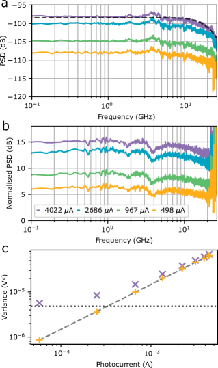
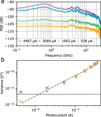
We perform a bandwidth measurement by optimising coupling at maximum power using the monitored photocurrent, then recording a series of spectra on the ESA as the VOA adjusts the input power from 13.5 dBm to -26.5 dBm. We also record the ESA displayed average noise level (DANL, the intrinsic ESA noise) for later subtraction from the data. All spectra are recorded at 100 kHz RBW over a 26.5 GHz span. The results of this are plotted in Figure 2. By fitting the detector response to a second-order Butterworth response, we obtain a 3-dB bandwidth of GHz. As the clearance of the detector extends beyond the bandwidth of our ESA, we estimate the shot noise bandwidth using Eq. A Bi-CMOS electronic-photonic integrated circuit quantum light detector. We fit the clearance of the detector with where describes the optical shot noise, the white noise terms of Equation A Bi-CMOS electronic-photonic integrated circuit quantum light detector and the latter frequency dependent terms (see Appendix). The fit suggests that the shot noise clearance extends far beyond the measured bandwidth, vanishing beyond 100 GHz. In practice we anticipate the photodiode transit time bandwidth to become limiting [36].
Grating coupler losses are measured using grating-to-grating test structures that we included on the ePIC chip. This yields an average of approximately dB per coupler. We characterise the photodiode responsivity by comparing the sum of measured photocurrents to off-chip LO power and correcting for grating coupler losses. From this, we obtain a maximum photodiode responsivity of 0.47 A/W at 2 V bias, including MMI insertion loss.
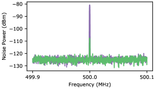
CMRR measurements are made by intensity-modulating the LO using an electro-optic modulator and comparing the signal with either both photodiodes biased as above, or one biased and the other disconnected to eliminate its photocurrent contribution. The ESA is set to 10 kHz RBW and a span of the modulation frequency. We observe a CMRR of 27 dB at 500 MHZ (Figure 3), which is limited by the intrinsic splitting ratio of our MMI. In future devices, this value can be improved by substituting the current static MMIs with thermoelectric tuneable Mach-Zehnder interferometers [23].
An ePIC quantum light detector is reported, combining photonics and readout electronics within a 80 m 220 m footprint. This was achieved thanks to the CMOS compatibility of silicon photonics, which can benefit the scalability and manufacturability of photonic quantum information processors and could be a potential necessity when considering the stringent timing limits imposed by feed-forward and delay lines [37]. The detector’s GHz 3-dB bandwidth is an order of magnitude greater than previous fastest demonstrations and surpasses the speed performance limits of homodyne detectors constructed from macroscopic wirebond interconnects [23]. The demonstration maintained shot noise efficiencies of at least 95%. Higher gains, and thus higher efficiencies, will be possible in future devices through multi-stage amplifier designs without sacrificing bandwidth [31]. Higher responsivity photodiodes have been demonstrated in silicon photonics, achieving 95% quantum efficiency with 30 GHz bandwidths in classical appliations [38], and fibre-coupling efficiencies of 95% have been observed with edge couplers [39]. Incorporating such improvements will enable ePIC detectors to simultaneously meet all of the performance requirements of future quantum technologies. We believe the current detector’s footprint and performance already opens application of ePIC homodyne detectors to minaturised and high speed receivers for quantum communications [18, 22], higher clock rates cluster state characterisation [16, 17] and large arrays of coherent receivers for continuous variables photonic quantum computing [4] and photonic neural networks operating below the Landauer limit [40].
Beyond detectors, we anticipate future applications of ePICs to increase the performance of quantum device control, including increasing the number of simultaneously controlled phase shift parameters beyond O() in highly programmable quantum devices [41]. We expect the combination of minaturised readout and control within ePICs will reduce the requirements on optical delay lines for quantum technologies utilising state-measurement and feedforward [37]. This is important for large-scale implementations of quantum technology including, multiplexed sources of quantum states [42], quantum state engineering [43] and measurement-based and time-multiplexed quantum computing [4, 44].
References
- Wang et al. [2020] J. Wang, F. Sciarrino, A. Laing, and M. G. Thompson, Integrated photonic quantum technologies, Nature Photonics 14, 273–284 (2020).
- Moody et al. [2022] G. Moody et al., 2022 roadmap on integrated quantum photonics, Journal of Physics: Photonics 4, 012501 (2022).
- Rudolph [2017] T. Rudolph, Why I am optimistic about the silicon-photonic route to quantum computing, APL Photonics 2, 030901 (2017).
- Eli Bourassa et al. [2021] J. Eli Bourassa et al., Blueprint for a scalable photonic fault-tolerant quantum computer, Quantum 5, 392 (2021).
- Silverstone et al. [2016] J. W. Silverstone, D. Bonneau, J. L. O’Brien, and M. G. Thompson, Silicon quantum photonics, IEEE Journal of Selected Topics in Quantum Electronics 22, 390 (2016).
- Giewont et al. [2019] K. Giewont et al., 300-mm monolithic silicon photonics foundry technology, IEEE J. Sel. Top. Quanutm Electron. 25, 8200611 (2019).
- Silverstone et al. [2014] J. W. Silverstone et al., On-chip quantum interference between silicon photon-pair sources, Nature Photonics 8, 104 (2014).
- Gentry et al. [2015] C. M. Gentry et al., Quantum-correlated photon pairs generated in a commercial 45 nm complementary metal-oxide semiconductor microelectronic chip, Optica 2, 1065 (2015).
- Knoll et al. [2015] D. Knoll et al., High-performance photonic bicmos process for the fabrication of high-bandwidth electronic-photonic integrated circuits, in 2015 IEEE International Electron Devices Meeting (IEDM) (2015) pp. 15.6.1–15.6.4.
- Dziallas et al. [2022] G. Dziallas et al., A 56-Gb/s Optical Receiver With 2.08-A Noise Monolithically Integrated into a 250-nm SiGe BiCMOS Technology, IEEE Transactions on Microwave Theory and Techniques 70, 392 (2022).
- Gudyriev et al. [2019] S. Gudyriev et al., Coherent ePIC Receiver for 64 GBaud QPSK in 0.25 m Photonic BiCMOS Technology, Journal of Lightwave Technology 37, 103 (2019).
- Rogers et al. [2021] C. Rogers et al., A universal 3d imaging sensor on a silicon photonics platform, Nature 590, 256 (2021).
- Lvovsky et al. [2001] A. I. Lvovsky et al., Quantum state reconstruction of the single-photon fock state, Physical Review Letters 87, 050402 (2001).
- Tse et al. [2019] M. Tse et al., Quantum-enhanced advanced ligo detectors in the era of gravitational-wave astronomy, Physical Review Letters 123, 231107 (2019).
- Acernese et al. [2019] F. Acernese et al. (Virgo Collaboration), Increasing the astrophysical reach of the advanced virgo detector via the application of squeezed vacuum states of light, Phys. Rev. Lett. 123, 231108 (2019).
- Larsen et al. [2019] M. V. Larsen, X. Guo, C. R. Breum, J. S. Neergaard-Nielsen, and U. L. Andersen, Deterministic generation of a two-dimensional cluster state, Science 366, 369 (2019).
- Asavanant et al. [2019] W. Asavanant et al., Generation of time-domain-multiplexed two-dimensional cluster state, Science 366, 373 (2019).
- Lodewyck et al. [2007] J. Lodewyck et al., Quantum key distribution over 25 km with an all-fiber continuous-variable system, Phys. Rev. A 76, 042305 (2007).
- Masada et al. [2015] G. Masada et al., Continuous-variable entanglement on a chip, Nature Photonics 9, 316 (2015).
- Lenzini et al. [2018] F. Lenzini et al., Integrated photonic platform for quantum information with continuous variables, Science Advances 4 (2018).
- Raffaelli et al. [2018] F. Raffaelli et al., A homodyne detector integrated onto a photonic chip for measuring quantum states and generating random numbers, Quantum Science and Technology 3, 025003 (2018).
- Zhang et al. [2019] G. Zhang et al., An integrated silicon photonic chip platform for continuous-variable quantum key distribution, Nature Photonics 13, 839 (2019).
- Tasker et al. [2021] J. F. Tasker, J. Frazer, et al., Silicon photonics interfaced with integrated electronics for 9 GHz measurement of squeezed light - Nature Photonics, Nat. Photonics 15, 11 (2021).
- Bruynsteen et al. [2021] C. Bruynsteen, M. Vanhoecke, J. Bauwelinck, and X. Yin, Integrated balanced homodyne photonic–electronic detector for beyond 20 ghz shot-noise-limited measurements, Optica 8, 1146 (2021).
- Stojanović et al. [2018] V. Stojanović et al., Monolithic silicon-photonic platforms in state-of-the-art CMOS SOI processes, Opt. Express 26, 13106 (2018).
- Feilchenfeld et al. [2015] N. B. Feilchenfeld et al., An integrated silicon photonics technology for O-band datacom, in 2015 IEEE International Electron Devices Meeting (IEDM) (2015) pp. 25.7.1–25.7.4.
- Narasimha et al. [2008] A. Narasimha et al., A 40-Gb/s QSFP Optoelectronic Transceiver in a 0.13 m CMOS Silicon-on-Insulator Technology, in OFC/NFOEC 2008 - 2008 Conference on Optical Fiber Communication/National Fiber Optic Engineers Conference (2008) pp. 1–3.
- Buckwalter et al. [2012] J. F. Buckwalter, X. Zheng, G. Li, K. Raj, and A. V. Krishnamoorthy, A Monolithic 25-Gb/s Transceiver With Photonic Ring Modulators and Ge Detectors in a 130-nm CMOS SOI Process, IEEE Journal of Solid-State Circuits 47, 1309 (2012).
- Cressler [2013] J. D. Cressler, A retrospective on the SiGe HBT: What we do know, what we don’t know, and what we would like to know better, in 2013 IEEE 13th Topical Meeting on Silicon Monolithic Integrated Circuits in RF Systems (2013) pp. 81–83.
- Knoll et al. [2013] D. Knoll et al., Substrate Design and Thermal Budget Tuning for Integration of Photonic Components in a High-Performance SiGe:C BiCMOS Process, ECS Transactions 50, 297 (2013).
- Säckinger [2010] E. Säckinger, The transimpedance limit, IEEE Transactions on Circuits and Systems I: Regular Papers 57, 1848 (2010).
- Vokić et al. [2016] N. Vokić, P. Brandl, K. Schneider-Hornstein, B. Goll, and H. Zimmermann, 10 gb/s switchable binary/pam-4 receiver and ring modulator driver for 3-d optoelectronic integration, IEEE Journal of Selected Topics in Quantum Electronics 22, 344 (2016).
- Lischke et al. [2015] S. Lischke et al., High bandwidth, high responsivity waveguide-coupled germanium p-i-n photodiode, Opt. Express 23, 27213 (2015).
- Masalov et al. [2017] A. V. Masalov, A. Kuzhamuratov, and A. I. Lvovsky, Noise spectra in balanced optical detectors based on transimpedance amplifiers, Review of Scientific Instruments 88, 113109 (2017).
- Säckinger [2017] E. Säckinger, Analysis and Design of Transimpedance Amplifiers for Optical Receivers (John Wiley & Sons, Inc., 2017) p. 208.
- Liu et al. [1999] P.-L. Liu, K. J. Williams, M. Y. Frankel, and R. D. Esman, Saturation characteristics of fast photodetectors, IEEE Trans. Microwave Theory Tech. 47, 1297 (1999).
- Scott and Balram [2022] J. R. Scott and K. C. Balram, Timing constraints imposed by classical digital control systems on photonic implementations of measurement-based quantum computing, IEEE Transactions on Quantum Engineering 3, 1 (2022).
- Benedikovic et al. [2019] D. Benedikovic et al., 25 gbps low-voltage hetero-structured silicon-germanium waveguide pin photodetectors for monolithic on-chip nanophotonic architectures, Photon. Res. 7, 437 (2019).
- Bakir et al. [2010] B. Bakir et al., Low-loss ( 1 db) and polarization-insensitive edge fiber couplers fabricated on 200-mm silicon-on-insulator wafers, IEEE Photonics Technology Letters 22, 739 (2010).
- Hamerly et al. [2019] R. Hamerly, L. Bernstein, A. Sludds, M. Soljačić, and D. Englund, Large-scale optical neural networks based on photoelectric multiplication, Physical Review X 9, 021032 (2019).
- Vigliar et al. [2021] C. Vigliar et al., Error-protected qubits in a silicon photonic chip, Nature Physics 17, 1137 (2021).
- Xiong et al. [2016] C. Xiong et al., Active temporal multiplexing of indistinguishable heralded single photons, Nat. Commun. 7, 1 (2016).
- Cable and Dowling [2007] H. Cable and J. P. Dowling, Efficient generation of large number-path entanglement using only linear optics and feed-forward, Phys. Rev. Lett. 99, 163604 (2007).
- Takeda and Furusawa [2017] S. Takeda and A. Furusawa, Universal Quantum Computing with Measurement-Induced Continuous-Variable Gate Sequence in a Loop-Based Architecture, Phys. Rev. Lett. 119, 120504 (2017).
Acknowledgements: The authors thank K. Balram, A. Laing, J. Silverstone and J. Smith for insightful discussion. The authors are grateful for technical assistance from L. Kling and A. Murray and access to the University of Bristol Cleanroom.
This work was supported by the Centre for Nanoscience and Quantum Information (NSQI), the European Research Council starting grant ERC-2018-STG 803665 and EPSRC Quantum Technology Capital fund: Quantum Photonic Integrated Circuits (QuPIC) EP/N015126/1. J.T. acknowledges support from an EPSRC Doctoral Training Partnership (1942717) for the experiment and device design stage of the project. J.C.F.M. acknowledges support from a Philip Leverhulme Prize.
Data access statement: The data and code that support the plots within this paper and other findings of this study are available from the corresponding author upon reasonable request.
I Appendix
Current offset excess noise
Due to the MMI imbalance before the photodiodes, we observe a power dependent net current offset, , at the amplifier input. This results in excess electronic noise at the amplifier output which we attribute to a combination of LO relative intensity noise and the amplifier’s DC current dependent gain. Figure A1 shows characterisation of the detector with symmetric 2 V reverse biases on each photodiode.
Shot noise clearance limit
The clearance of a balanced homodyne detector is described by a function of the form,
| (4) |
where describes the shot noise contribution and and represent the white noise and quadratic noise terms of Equation 2 in the main text [34]. We fit this function to the measured clearance data, plotting the data and fit in Figure A2.
1
