Germanium wafers for strained quantum wells with low disorder
Abstract
We grow strained Ge/SiGe heterostructures by reduced-pressure chemical vapor deposition on 100 mm Ge wafers. The use of Ge wafers as substrates for epitaxy enables high-quality Ge-rich SiGe strain-relaxed buffers with a threading dislocation density of , nearly an order of magnitude improvement compared to control strain-relaxed buffers on Si wafers. The associated reduction in short-range scattering allows for a drastic improvement of the disorder properties of the two-dimensional hole gas, measured in several Ge/SiGe heterostructure field-effect transistors. We measure an average low percolation density of , and an average maximum mobility of and quantum mobility of when the hole density in the quantum well is saturated to . We anticipate immediate application of these heterostructures for next-generation, higher-performance Ge spin-qubits and their integration into larger quantum processors.
Strained germanium quantum wells in silicon-germanium heterostructures (Ge/SiGe) have become the leading platform for quantum computation with hole spin qubits.Scappucci et al. (2021) Single-hole spin qubits and singlet-triplet qubits can be universally controlled,Hendrickx et al. (2020); Jirovec et al. (2021); Wang et al. (2022) four-qubit logic has been executed,Hendrickx et al. (2021) and quantum dot systems have been scaled to crossbar arrays comprising 16 quantum dots.Borsoi et al. (2022) Furthermore, the demonstration of a hard superconducting gap in GeTosato et al. (2023) motivates the pursuit of coherent coupling of high fidelity Ge spin qubits using crossed Andreev reflection for achieving two-qubit gates over micrometer distances.Choi et al. (2000); Leijnse and Flensberg (2013) While single-spin qubits have been operated with fidelity as high as 99.99%,Lawrie et al. (2021) and rudimentary error correction circuits have been executed,van Riggelen et al. (2022) quantum coherence limits the operation of larger systems. Although Ge can be isotopically enriched to remove dephasing due to hyperfine interaction,Itoh et al. (1993) which can also be achieved by strong confinement,Bosco and Loss (2021) hole spin qubits are highly sensitive to charge noise, strain fluctuations, and other types of disorder that can affect the spin-orbit interactions.Bosco et al. (2021); Malkoc et al. (2022); Terrazos et al. (2021); Abadillo-Uriel et al. (2022) In addition to optimizing the semiconductor-dielectric interface in qubit devices, further improving the crystalline quality of strained quantum wellsPaquelet Wuetz et al. (2023) appears as a key step to obtain a quieter environment for Ge quantum dots.
In the absence of suitable SiGe wafers for high-quality and uniform epitaxy, strained Ge quantum wells are commonly deposited on strain-relaxed buffers (SRBs) with high Ge composition ().Scappucci et al. (2021) Starting epitaxy from a Si wafer, Ge-rich SiGe SRBs are obtained by composition grading either in a forward-graded processIsella et al. (2004) or in a reverse-graded process after the deposition of a thick strain-relaxed Ge layer.Shah et al. (2008); Sammak et al. (2019) In both cases, the large lattice mismatch between the Si substrate and the Ge-rich SiGe SRB causes a dense misfit dislocation network, with associated threading dislocations that propagate through the quantum well. Moreover, such misfit dislocation network drives significant local strain fluctuations inside the Ge quantum well,Corley-Wiciak et al. (2023), thus challenging the scalability of semiconductor qubits. In Ge/SiGe heterostructures used to host qubits, the threading dislocation density (TDD) is in the range cm-2.Sammak et al. (2019); Jirovec et al. (2021) It is not surprising that Si/SiGe heterostructures have smaller TDD ( cm-2) because the Si-rich SiGe SRBs have less lattice mismatch to the Si substrate due to the smaller Ge composition (). In this Letter we depart from Si wafers and investigate Ge/SiGe heterostructures grown directly on Ge wafers, mitigating the complication of a large lattice-mismatch between Ge-rich SiGe and Si wafers. As a result, we show a significant enhancement of the crystal quality of the heterostructure, as well as a drastic improvement in the disorder properties of the two-dimensional hole gas (2DHG) that it supports.
Schematics in Figs. 1(a) and (b) compare heterostructures on a Ge wafer with our control reverse-graded heterostructures on a Si wafer,Lodari et al. (2021) the same that supported a four qubit quantum processor and a 16 quantum dot crossbar array.Hendrickx et al. (2021); Borsoi et al. (2022) The 100 mm Ge wafers are prepared for epitaxy by an ex-situ HF-dip etch followed by in-situ bake at . The heterostructure is grown in a high-throughput reduced-pressure chemical vapor deposition tool from high-purity germane and dichlorosilane. The SiGe SRB is thick and obtained by forward step grading of the Si content (). This approach mirrors the common approach in Si/SiGe heterostructures where the Ge content is forward-graded starting from a Si wafer. Like our previous heterostructures,Sammak et al. (2019) the SiGe SRB is deposited at and the growth temperature is reduced to for the final 200 nm of SiGe below the quantum well and for all the layers above to achieve sharp quantum well interfaces. Importantly, by growing on Ge wafers we avoid the overtensile strain arising from the difference in the thermal expansion coefficients between Ge epilayers and Si substrates.Shah et al. (2008) Consequently, to achieve an in-plane strain () in the Ge quantum well similar to our previous heterostructures,Sammak et al. (2019); Lodari et al. (2021) here we increase the final Ge content in the SRB to 0.83 (the supplementary material) compared to 0.8 in Refs. Sammak et al. (2019); Lodari et al. (2021)). The thickness of the Ge quantum well (16 nm) and of the SiGe barrier on top (55 nm) are nominally the same compared to Ref. Lodari et al. (2021) for a meaningful comparison of the electrical transport properties.
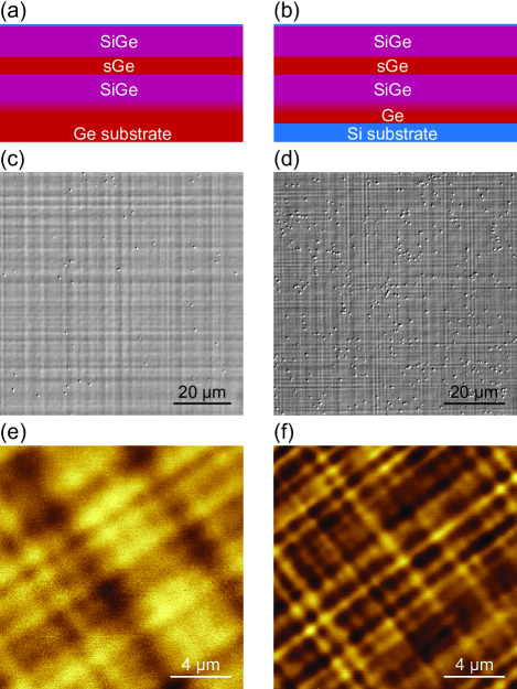
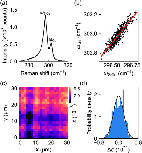
Figure 1(c) and (d) show comparative images by Nomarski microscopy of the heterostructures on a Ge and on a Si wafer after decorating the threading dislocations by in-situ HCl vapor etching.Bogumilowicz et al. (2005) We quantify the TDD by counting the number of decorated threading dislocations from multiple images taken across the wafer. Changing substrate from Si to Ge improves the TDD almost an order of magnitude, from to . Consequently the average TD separation () becomes much longer, from to . Comparative atomic-force microscopy images in Figs. 1(e) and (f) show the typical cross hatch pattern arising from the strain-releasing misfit dislocation network within the SiGe SRB on Ge and Si wafers, respectively. The root mean square surface roughness of both heterostructures is similar at 1.5 nm. However, the heterostructure grown on a Ge wafer shows cross-hatch undulations with a longer wavelength and weaker high-frequency components of the Fourier spectrum (the supplementary material). This observation supports the intuition that the Ge-rich SiGe SRB has a less dense network of misfit dislocations when grown on a Ge wafer, as the lattice mismatch with the substrate is smaller compared to when it is grown on a Si wafer.
We further characterize the heterostructure on the Ge wafer by scanning Raman spectroscopy over an area of , much larger than the length scale of the cross-hatch pattern features. In particular, we determined the in-plane strain in the quantum well and analyzed the origin and bandwidth of its fluctuations. The representative spectrum in Fig. 2(a) was obtained with a 633 nm red laser and shows two clear Raman peaks originating from the Ge-Ge vibration modes in the strained Ge quantum well () and in the SiGe layer (). The distribution of these Raman shifts in Fig. 2(b) shows a strong correlation, with a slope . Comparing to predictions by Eq. 5 in Ref. Kutsukake et al. (2004), we argue that the distribution of the Raman shift in the Ge quantum well is mainly driven by strain fluctuations in the SiGe SRB (expected ), rather than compositional fluctuations (). Figure 2(c) shows the Raman strain map of the Ge quantum well calculated using , where is the Raman shift for bulk Ge and is the Ge phonon strain shift coefficient.Pezzoli et al. (2008) We identify signatures of the cross-hatch pattern, with regions featuring higher and lower strain around a mean strain value . This is similar to the compressive strain measured in our Ge quantum wells on a Si wafer,Sammak et al. (2019) validating our heterostructure design and comparative analysis. The statistics of the lateral strain map are shown in Fig. 2d. The strain fluctuations around the average follow a normal distribution with a standard deviation of . The bandwidth of the strain fluctuations is reduced when compared to the strain fluctuations from the heterostructure on a Si wafer,Corley-Wiciak et al. (2023) pointing to a more uniform strain landscape.
The structural characterization highlights the improvement in crystal quality when growing a Ge-rich SRB on a Ge wafer instead of a Si wafer. Next, we show how a better and more uniform crystalline environment improves the disorder properties of the 2DHG. We fabricate six Hall-bar shaped heterostructure field effect transistors (H-FETs) on a cm2 coupon from the center of the 100 mm wafer with a similar process as in Ref. Lodari et al. (2021) We accumulate a 2DHG inside the Ge quantum well by applying a negative DC gate voltage () to the top gate of the H-FETs and we increase the density in the 2DHG above the percolation density () by making more negative. We use standard four-probe low-frequency lock-in techniques for mobility-density and magnetotransport characterization of all devices in a dilution refrigerator equipped with a cryo-multiplexerPaquelet Wuetz et al. (2020) ( mK measured at the mixing chamber).
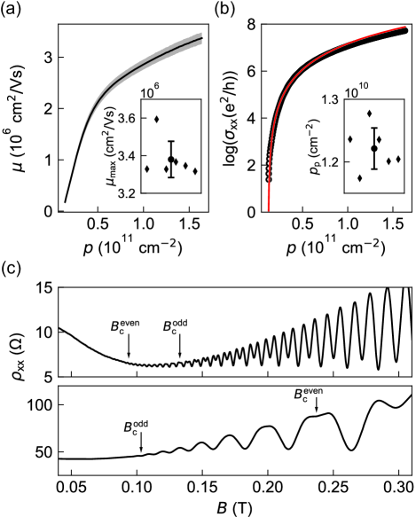
Figure 3(a) shows the density-dependent mobility curve (solid line), obtained by averaging over the six H-FETs, together with the standard deviation (shaded region). We observe a tight distribution over the entire density range, indicating a very uniform disorder potential landscape. The mobility increases steeply with increasing density, due to increasing screening of the remote impurity charges, most likely at the semiconductor-dielectric interface. At higher densities (), the mobility increases less rapidly, signaling the relevance of scattering from impurities within or in the proximity of the quantum well.Monroe (1993) We observe a maximum mobility in the range of over the six investigated H-FETS (Fig. 3(a), inset), from which we extract an average at a saturation density , corresponding to a long mean free path of . Figure 3b shows the longitudinal conductivity as a function of density for a representative H-FET. We extract the percolation density from fitting to percolation theory,Tracy et al. (2009) . The inset shows for the six H-FETs, from which we extract an average percolation density .
Compared to our control heterostructures on a Si wafer supporting qubits,Lodari et al. (2021); Hendrickx et al. (2021) the maximum mobility is more than 15 times larger and the percolation density is more than 1.5 times smaller. We speculate that this significant improvement, throughout the whole density range, is associated with the suppression of short-range scattering from dislocations within the quantum well. Furthermore, the mobility has not yet saturated indicating that it is still limited by long-range scattering from impurities at the dielectric interface, leaving room for further improvement. In fact, our maximum mobility, reproducible across multiple devices, is less than the value measured on a single H-FET in Ge/SiGe grown on a Si wafer,Myronov et al. (2023) likely because the dielectric interface in our samples is much closer to the channel (55 nm compared to 100 nm in Ref. Myronov et al. (2023)).
The low level of disorder is confirmed by high-quality magnetotransport characterization observed in all devices. Figure 3(c) shows representative magneto-resistivity curves from an H-FET at fixed densities of (upper panel) and (lower panel). The measurements were performed by keeping constant and sweeping the perpendicular magnetic field . For each longitudinal resistivity () curve we extract the pair of critical magnetic fields for resolving the cyclotron and the spin gap, , corresponding, respectively, to even and odd filling factors in the Shubnikov –de Haas oscillations minima. Due to the very small Landau level broadening at high density, the cyclotron gap (see upper panel of Fig. 3(c)) is resolved already at very low critical fields and the spin gap only a few oscillations later, . However, at low density the order is reversed and the spin gap is resolved earlier than the cyclotron gap, (see lower panel of Fig. 3(c)). This is typical to 2DHGs in Ge/SiGe and occurs when the spin gap is more than half of the cyclotron gap, due to the increased perpendicular -factors of holes at low density.Lu et al. (2017); Lodari et al. (2019); Myronov et al. (2023)
The combination of these two aspects, the very low level of disorder and the increasingly large spin gap at low density, makes the canonical methodsColeridge (1991); Coleridge et al. (1996) for extracting the effective mass and single-particle lifetime not straightforward throughout the investigated density range and will be pursued in a further study. However, we may still estimate the quantum mobility without making assumptions on and using the expression (the supplementary material). With this analysis, we obtain a maximum quantum mobility in the range of over the six investigated H-FETS (the supplemental material), from which we extract an average maximum at saturation density. This value should be considered as a conservative estimate of , as the onset of Shubnikov –de Haas oscillations in our high-quality samples might be limited by small density inhomogeneities at low magnetic field.Qian et al. (2017) The maximum is over three times larger than that of our control heterostructures on a Si wafer,Lodari et al. (2021); Hendrickx et al. (2021) and approximately two times larger compared to the heterostructures on a Si wafer in Ref. Myronov et al. (2023) These results highlight the significantly improved short-range scattering in 2DHGs when the Ge-rich SiGe SRB is grown on a Ge substrate, setting a benchmark for holes in group IV semiconductors.
In summary, we challenged the mainstream approach to deposit Ge/SiGe heterostructures on Si wafers and instead, we started epitaxy on a Ge wafer. We demonstrate a more uniform crystalline environment with fewer dislocations and in-plane strain fluctuations compared to control heterostructures supporting a four-qubit quantum processors. Future investigations using X-ray diffraction spectroscopy to map the complete strain tensorCorley-Wiciak et al. (2023) could provide insights into the local strain modifications and fluctuation caused by nanostructured metallic gates. The disorder properties of the 2DHG are also greatly improved, with reproducible ultra-high mobility, very low percolation density, and high quantum mobility. Considering these heterostructures on Ge wafers as a proof of principle, the electrical transport metrics are likely to further improve by routine optimization of the heterostructure design and chemical vapor deposition process. We anticipate immediate benefit of using these heterostructures for improved uniformity and yield in large quantum dot arrays. Future studies on charge noise and qubit performance may also provide insight in possible improved quantum coherence. Furthermore, it would be of significant interest to explore whether suppressing the dislocation network in the SiGe SRB could improve the performance of superconducting microwave resonators integrated atop the heterostructure, towards the development of hybrid superconductor-semiconductor architectures.
See the supplementary material for secondary ions mass spectroscopy, Fourier transform of the atomic force microscopy images, and the derivation of the expression for quantum mobility.
This work was supported by the Netherlands Organisation for Scientific Research (NWO/OCW), as part of the Frontiers of Nanoscience program. A.T. acknowledges support through a projectruimte associated with the Netherlands Organization of Scientific Research (NWO). This research was supported by the European Union’s Horizon 2020 research and innovation programme under the grant agreement No. 951852.
Author Declarations
The authors have no conflict to disclose
Data availability
The data sets supporting the findings of this study are openly available in 4TU Research Data at https://doi.org/10.4121/52a5bcf9-8e15-4871-b256-10f90e320ecc, Ref Stehouwer and Scappucci (2023).
References
- Scappucci et al. (2021) G. Scappucci, C. Kloeffel, F. A. Zwanenburg, D. Loss, M. Myronov, J.-J. Zhang, S. De Franceschi, G. Katsaros, and M. Veldhorst, Nature Reviews Materials 6, 926 (2021).
- Hendrickx et al. (2020) N. W. Hendrickx, W. I. L. Lawrie, L. Petit, A. Sammak, G. Scappucci, and M. Veldhorst, Nature Communications 11, 3478 (2020).
- Jirovec et al. (2021) D. Jirovec, A. Hofmann, A. Ballabio, P. M. Mutter, G. Tavani, M. Botifoll, A. Crippa, J. Kukucka, O. Sagi, F. Martins, J. Saez-Mollejo, I. Prieto, M. Borovkov, J. Arbiol, D. Chrastina, G. Isella, and G. Katsaros, Nature Materials 20, 1106 (2021).
- Wang et al. (2022) C.-A. Wang, C. Déprez, H. Tidjani, W. I. L. Lawrie, N. W. Hendrickx, A. Sammak, G. Scappucci, and M. Veldhorst, npj Quantum Information 9, 58 (2023).
- Hendrickx et al. (2021) N. W. Hendrickx, W. I. L. Lawrie, M. Russ, F. van Riggelen, S. L. de Snoo, R. N. Schouten, A. Sammak, G. Scappucci, and M. Veldhorst, Nature 591, 580 (2021).
- Borsoi et al. (2022) F. Borsoi, N. W. Hendrickx, V. John, S. Motz, F. van Riggelen, A. Sammak, S. L. de Snoo, G. Scappucci, and M. Veldhorst, Preprint at https://arxiv.org/abs/2209.06609 (2022).
- Tosato et al. (2023) A. Tosato, V. Levajac, J.-Y. Wang, C. J. Boor, F. Borsoi, M. Botifoll, C. N. Borja, S. Martí-Sánchez, J. Arbiol, A. Sammak, M. Veldhorst, and G. Scappucci, Communications Materials 4, 23 (2023).
- Choi et al. (2000) M.-S. Choi, C. Bruder, and D. Loss, Physical Review B 62, 13569 (2000).
- Leijnse and Flensberg (2013) M. Leijnse and K. Flensberg, Physical Review Letters 111, 060501 (2013).
- Lawrie et al. (2021) W. I. L. Lawrie, M. Russ, F. van Riggelen, N. W. Hendrickx, S. L. de Snoo, A. Sammak, G. Scappucci, J. Helsen, and M. Veldhorst, Nature Communications 14, 3617 (2023).
- van Riggelen et al. (2022) F. van Riggelen, W. I. L. Lawrie, M. Russ, N. W. Hendrickx, A. Sammak, M. Rispler, B. M. Terhal, G. Scappucci, and M. Veldhorst, npj Quantum Information 8, 124 (2022).
- Itoh et al. (1993) K. Itoh, W. L. Hansen, E. E. Haller, J. W. Farmer, V. I. Ozhogin, A. Rudnev, and A. Tikhomirov, Journal of Materials Research 8, 1341 (1993).
- Bosco and Loss (2021) S. Bosco and D. Loss, Physical Review Letters 127, 190501 (2021).
- Bosco et al. (2021) S. Bosco, B. Hetényi, and D. Loss, PRX Quantum 2, 010348 (2021).
- Malkoc et al. (2022) O. Malkoc, P. Stano, and D. Loss, Physical Review Letters 129, 247701 (2022).
- Terrazos et al. (2021) L. A. Terrazos, E. Marcellina, Z. Wang, S. N. Coppersmith, M. Friesen, A. R. Hamilton, X. Hu, B. Koiller, A. L. Saraiva, D. Culcer, and R. B. Capaz, Physical Review B 103, 125201 (2021).
- Abadillo-Uriel et al. (2022) J. C. Abadillo-Uriel, E. A. Rodríguez-Mena, B. Martinez, and Y.-M. Niquet, Preprint at https://arxiv.org/abs/2212.03691 (2022), 10.48550/arXiv.2212.03691.
- Paquelet Wuetz et al. (2023) B. Paquelet Wuetz, D. Degli Esposti, A.-M. J. Zwerver, S. V. Amitonov, M. Botifoll, J. Arbiol, A. Sammak, L. M. K. Vandersypen, M. Russ, and G. Scappucci, Nature Communications 14, 1385 (2023).
- Isella et al. (2004) G. Isella, D. Chrastina, B. Rössner, T. Hackbarth, H.-J. Herzog, U. König, and H. Von Känel, Solid-State Electronics 48, 1317 (2004).
- Shah et al. (2008) V. A. Shah, A. Dobbie, M. Myronov, D. J. F. Fulgoni, L. J. Nash, and D. R. Leadley, Applied Physics Letters 93, 192103 (2008).
- Sammak et al. (2019) A. Sammak, D. Sabbagh, N. W. Hendrickx, M. Lodari, B. Paquelet Wuetz, A. Tosato, L. Yeoh, M. Bollani, M. Virgilio, M. A. Schubert, P. Zaumseil, G. Capellini, M. Veldhorst, and G. Scappucci, Advanced Functional Materials 29, 1807613 (2019).
- Corley-Wiciak et al. (2023) C. Corley-Wiciak, C. Richter, M. H. Zoellner, I. Zaitsev, C. L. Manganelli, E. Zatterin, T. U. Schülli, A. A. Corley-Wiciak, J. Katzer, F. Reichmann, W. M. Klesse, N. W. Hendrickx, A. Sammak, M. Veldhorst, G. Scappucci, M. Virgilio, and G. Capellini, ACS Applied Materials & Interfaces 15, 3119 (2023).
- Lodari et al. (2021) M. Lodari, N. W. Hendrickx, W. I. L. Lawrie, T.-K. Hsiao, L. M. K. Vandersypen, A. Sammak, M. Veldhorst, and G. Scappucci, Materials for Quantum Technology 1, 011002 (2021).
- Bogumilowicz et al. (2005) Y. Bogumilowicz, J. M. Hartmann, R. Truche, Y. Campidelli, G. Rolland, and T. Billon, Semiconductor Science and Technology 20, 127 (2005).
- Kutsukake et al. (2004) K. Kutsukake, N. Usami, T. Ujihara, K. Fujiwara, G. Sazaki, and K. Nakajima, Applied Physics Letters 85, 1335 (2004).
- Pezzoli et al. (2008) F. Pezzoli, E. Bonera, E. Grilli, M. Guzzi, S. Sanguinetti, D. Chrastina, G. Isella, H. Von Känel, E. Wintersberger, J. Stangl, and G. Bauer, Journal of Applied Physics 103, 093521 (2008).
- Paquelet Wuetz et al. (2020) B. Paquelet Wuetz, P. L. Bavdaz, L. A. Yeoh, R. Schouten, H. van der Does, M. Tiggelman, D. Sabbagh, A. Sammak, C. G. Almudever, F. Sebastiano, J. S. Clarke, M. Veldhorst, and G. Scappucci, npj Quantum Information 6, 43 (2020).
- Monroe (1993) D. Monroe, Journal of Vacuum Science & Technology B: Microelectronics and Nanometer Structures 11, 1731 (1993).
- Tracy et al. (2009) L. A. Tracy, E. H. Hwang, K. Eng, G. A. Ten Eyck, E. P. Nordberg, K. Childs, M. S. Carroll, M. P. Lilly, and S. Das Sarma, Physical Review B 79, 235307 (2009).
- Myronov et al. (2023) M. Myronov, J. Kycia, P. Waldron, W. Jiang, P. Barrios, A. Bogan, P. Coleridge, and S. Studenikin, Small Science 3, 2200094 (2023).
- Lu et al. (2017) T. M. Lu, L. A. Tracy, D. Laroche, S.-H. Huang, Y. Chuang, Y.-H. Su, J.-Y. Li, and C. W. Liu, Scientific Reports 7, 2468 (2017).
- Lodari et al. (2019) M. Lodari, A. Tosato, D. Sabbagh, M. A. Schubert, G. Capellini, A. Sammak, M. Veldhorst, and G. Scappucci, Physical Review B 100, 041304 (2019).
- Coleridge (1991) P. T. Coleridge, Physical Review B 44, 3793 (1991).
- Coleridge et al. (1996) P. T. Coleridge, M. Hayne, P. Zawadzki, and A. S. Sachrajda, Surface Science 361-362, 560 (1996).
- Qian et al. (2017) Q. Qian, J. Nakamura, S. Fallahi, G. C. Gardner, J. D. Watson, S. Lüscher, J. A. Folk, G. A. Csáthy, and M. J. Manfra, Physical Review B 96, 035309 (2017).
- Stehouwer and Scappucci (2023) L. Stehouwer and G. Scappucci, 4TU.ResearchData. Dataset (2023), 10.4121/52a5bcf9-8e15-4871-b256-10f90e320ecc.