Transporting cold atoms towards a GaN-on-sapphire chip via an optical conveyor belt
Abstract
Trapped atoms on photonic structures inspire many novel quantum devices for quantum information processing and quantum sensing. Here, we have demonstrated a hybrid photonic-atom chip platform based on a GaN-on-sapphire chip and the transport of an ensemble of atoms from free space towards the chip with an optical conveyor belt. The maximum transport efficiency of atoms is about with a transport distance of . Our results open up a new route toward the efficiently loading of cold atoms into the evanescent-field trap formed by the photonic integrated circuits, which promises strong and controllable interactions between single atoms and single photons.
I Introduction
By introducing neutral atoms to integrated photonic devices, the hybrid photonic-atomic chip (PAC) has attracted extensive research in recent years Chang et al. (2018); Luan et al. (2020); Béguin et al. (2020); Wang et al. (2022); Bouscal et al. (2023). Benefiting from the strongly enhanced light-matter interactions due to the tightly optical field confinement at the wavelength and even subwavelength scale, PAC holds great potential in many quantum-based applications, such as quantum memory Lvovsky et al. (2009); Gouraud et al. (2015), novel quantum light sources Pichler et al. (2017), chiral quantum optics devices Scheucher et al. (2016); Lodahl et al. (2017), nodes of quantum networks Kimble (2008); Tiecke et al. (2014); Muralidharan et al. (2017), novel quantum optics phenomena with surface plasmons Stehle et al. (2014, 2011), many-body physics Douglas et al. (2015); González-Tudela et al. (2015), and quantum sensing Zektzer et al. (2021); Sebbag et al. (2020).
Early efforts on trapping cold neutral atoms near surface microstructures was firstly explored above current carrying microstructures Lin et al. (2004); Fortágh et al. (2002), which can be tailored to create a variety of potential geometry and guiding schemes for cold atoms. Atoms are manipulated by the magnetic filed and the distances between the atoms and microstructures surface can be reduced to as close as Lin et al. (2004). With the advancement of fabrication techniques in photonic structures, manipulation of single atoms at wavelength and even subwavelength scale is possible with the tightly confined optical field confinement near the photonic structures. Many groundbreaking experimental results in coupling atoms to photonic structures have been achieved in various nanophotonic platforms Burgers et al. (2019); Thompson et al. (2013); Samutpraphoot et al. (2020); Ðorđević et al. (2021); Kim et al. (2019); Zhou et al. (2023); Aoki et al. (2006); Will et al. (2021); Vetsch et al. (2010); Goban et al. (2012); Gouraud et al. (2015); Corzo et al. (2019). However, these researches move forward with some potential disadvantages. For instance, the platforms based on nanofibers Vetsch et al. (2010); Goban et al. (2012); Gouraud et al. (2015); Corzo et al. (2019) are suspended in vacuum, thus are potentially unstable and have poor thermal conductivity, which imposes limitations on the atom trap lifetime and atom coherence time Reitz et al. (2013); Hümmer et al. (2019). Besides, vacuum feedthrough for the coupling of light in and out of the nanofiber brings complexity in fiber alignment and assembly. Other platforms based on solid-state microcavities, such as microtoroid or bottle microresonators Aoki et al. (2006); Shomroni et al. (2014); Scheucher et al. (2016); Will et al. (2021), unable to directly load laser cooled atoms into the evanescent-field trap Barnett et al. (2000), face difficulties in deterministic loading and trapping of cold atoms. Although the reported single atom-photon interaction time has been improved from only a few microseconds Aoki et al. (2006) to Will et al. (2021), the further extension of the system to more photonic structures and more atoms is very challenging.
In order to achieve deterministic atom trapping on integrated photonic devices, important theoretical and experimental milestones have been reached with unsuspended waveguide and microring structures Burgers et al. (2019); Thompson et al. (2013); Samutpraphoot et al. (2020); Ðorđević et al. (2021); Kim et al. (2019); Chang et al. (2019); Zhou et al. (2023); Liu et al. (2022a). Atoms are loaded into the evanescent field of the photonic structures from free space with optical tweezers and optical conveyor belts. These methods exhibit a highly precise control of atomic motion near photonic structures, including photonic crystal waveguides Burgers et al. (2019); Thompson et al. (2013); Samutpraphoot et al. (2020); Ðorđević et al. (2021) and microring resonators Kim et al. (2019); Chang et al. (2019); Zhou et al. (2023). Additionally, these demonstrations are compatible with on-chip integrated devices for cooling, transport, and trapping of cold atoms Liu et al. (2022b); Meng et al. (2015); Chen et al. (2022).
In this work, we report on transporting free space cooled 87Rb atoms towards a GaN-on-sapphire chip Liu et al. (2022a) with an optical conveyor belt Burgers et al. (2019); Kuhr et al. (2001); Nussmann et al. (2005); Dinardo and Anderson (2016). The conveyor belt consists of two focused beams, both beams passing through the sapphire substrate perpendicularly. After careful spatial calibration of the beams and phase stabilization, our conveyor belt directly transports trapped atoms with a temperature around toward the chip, without extra aberration of the focus beam from the sapphire substrate. The maximum transport efficiency of atoms is about with a transport distance of . It paves the way for the further implementation of stable atom trapping on the GaN-on-sapphire chip, promotes the realization of deterministic loading of atoms into the evanescent-field trap, which are promising for realizing the on-chip single-photon-level optical nonlinearity.
II Overview of the photonic-atom chip
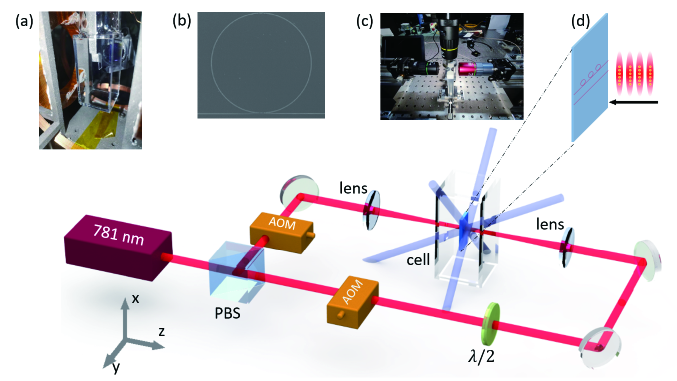
Figure 1 illustrates our experimental setup for studying the PAC, where a GaN-on-sapphire chip is placed inside the vacuum cell (). Figure 1(a) shows a photograph of our PAC platform in a vacuum cell. We use low vapor pressure epoxy (Torr Seal) to stick the chip onto a metal holder while maintaining high vacuum and enduring the high temperature during the vacuum baking process. Half of the chip without fabrication is glued onto a 316-L stainless steel holder, and the remaining part of the chip is suspended in vacuum with waveguide and microring resonator structures fabricated on the surface. The metal holder is then connected to a CF35 vacuum cube, providing heat dissipation and stability for the chip.
Figure 1(b) shows the scanning electron microscope (SEM) image of a fabricated microring resonator and the bus waveguides on top of the GaN-on-sapphire chip. The size of the sapphire substrate is . The microring resonator is vacuum-cladded for direct interaction between atoms and the evanescent field of the confined modes, with a major radius of and a cross-section of , and the optical modes of the microring are coupled to a bus waveguide through the evanescent field. Such microring resonators have been widely studied in photonics applications, due to their easy fabrication, high quality factor and small mode volume Liu et al. (2022c). Here, we adapt the GaN-on-sapphire platform for PAC following our previous theoretical proposal Liu et al. (2022a), as the system is more stable without suspended photonic structures. In addition, both GaN and sapphire are wide-band-gap materials that are transparent to ultrabroadband wavelengths (260 - 1590 nm) Yu et al. (1997); Muth et al. (1999), thus our chip is compatible with lasers working in the visible and near-visible wavelengths for many alkali and alkaline-earth atoms, allowing full optical access for cold rubidium atom cooling, trapping, transport and detection. The realization of the on-chip single-photon-level optical nonlinearity highly depends on the cooperativity parameter , where is the wavelength of the D2 line of rubidium atoms. The cooperativity parameter is proportional to the ratio of the quality factor and the mode volume for the microring resonator . For our microring resonator parameter, the currently achieved quality factor , mainly limited by the surface roughness.
As shown in Fig. 1, our optical configurations of the experiments could be divided into three parts: (i) coupling to PAC, (ii) magneto-optical trap (MOT) , and (iii) optical conveyor belt. First, at both ends the GaN-on-sapphire chip, light is coupled in and out of the photonic chip through a high numerical aperture (N.A.) objectives. Figure 1(c) shows the photograph of our testing setup for the coupling to PAC. A coupling efficiency of about for the GaN waveguide in Fig. 1(b) for optical signals with wavelength can be achieved with commercial objectives.
The cold 87Rb atoms are then prepared through a standard six-beam magneto-optical trap Metcalf and van der Straten (1999). The glass cell is connected to a mini cube and a ion pump, resulting in a pressure of mbar measured by the ion-pump current. Three pairs of cooling laser beams are generated from a laser, with the power of each beam being about and the beam waist being . The cooling laser beam is red detuned by from the D2 cycling transition. Additionally, of repump laser beams overlap with one of the cooling laser beams. The beams intersect at one point about above the surface of the chip, with additional anti-Helmholtz coils aligned with the point providing a magnetic field gradient up to . To align with our PAC, two pairs of cooling laser beams with a crossing angle of 60 degree in the X-Y plane go parallel to the chip surface, while the third pair passes through the crossing of the beams in the X-Y plane and the chip surface at an angle of 60 degree to the chip surface. Although MOT beam pairs are not oriented orthogonal to each other, 3D atom confinement is still achieved as components of each beam are projected along the orthogonal axis.
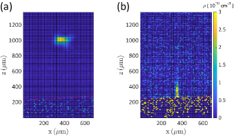
Following the 3D MOT procedure, the temperature of the atom ensemble around is finally achieved by a polarization-gradient cooling (PGC) process. With a duration of for the PGC, the cooling laser beams detuning is ramped down to from the cycling transition. Figure 2(a) shows a density contour plot of the atom ensemble, which is deduced from a single shot free space absorption imageKetterle et al. (1999). The cold atoms are about away from the chip surface, and the atom number density is about with an atom cloud radius about . The distance between the atom cloud and the chip surface can be adjusted from to by adjusting the offset coil and the alignment of the cooling beams. However, in close proximity to the chip, the density and shape of the atomic cloud is altered due to surface reflections, which is consistent with previous observationsHuet et al. (2012).
III Transporting atoms towards the chip
The optical conveyor belt is realized by an optical dipole trap, which consists of two linearly polarized counter-propagating Gaussian beams with beam waist , and the waist is located in the middle of the MOT atom cloud and the chip surface. The intensities of both beams are equal, and their optical frequencies are different by detuning . The two counterpropagating dipole laser beams come from a single laser, with corresponding to a frequency red detuned to the 87Rb atom D2 transition. The laser is split into two paths and then passed through a double-pass 80 MHz acousto-optic modulator (AOM), with controllable via the RF signals applied to the AOMs. Therefore, the two beams generate a spatially and temporally varying trap potential , where is the local trap depth and is the position of atoms along the beam axis. Trapped atoms are confined in the lattice antinodes and moved with the temporally varying trap potential (see Fig. 1(d)).
In order to transport atoms towards the surface of the PAC, we first load approximately atoms into a standing-wave dipole trap with by overlapping both dipole beams with the 3D MOT for . Here, each beam has a power of , which corresponds to a trap depth of about . After the loading process, atoms are trapped in a series of lattice antinodes along the beam axis, with an axial distribution of about limited by the size of the atom cloud. Then, a frequency chirping sequence of (see the inset of Fig. 3(a)), which is achieved by the sweep mode of the signal generator, is sent to one of the AOMs to create a moving optical conveyor belt, and the antinodes move at a velocity Kuhr et al. (2001)
| (1) |
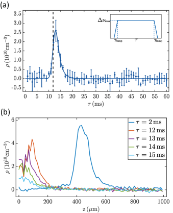
To verify the transport of atoms towards the chip surface, we take an absorption image of cold atoms in the optical conveyor belt after the transport process. Figure 2(b) shows the results indicating the ensemble of atoms near the chip surface (the dashed red line). Compared with the image of the atom cloud prepared by MOT, our conveyor belt has successfully delivered atoms towards the chip. Then, the transport of atoms in the optical conveyor belt is systematically investigated. Through a sequence of , as illustrated by the inset of Fig. 3(a), we could transport the atoms over a certain distance by ramping up in to , holding the detuning for a duration of , and then ramping down in . The distance . Figure 3(a) summarizes the measured atomic density on the chip surface for different hold times , with and a maximum transport distance limited by the block of the chip. We observed a clear atomic density peak of when , which almostly agrees with the calculated time (dashed vertical line) for transporting atoms from the center of the MOT to the chip surface.
The accumulation of atomic density on the chip surface can be described by a simple rate equation
| (2) |
where describes the atomic flux to the chip surface by the optical conveyor belt and is the linear atomic loss coefficient. Here, is mainly attributed to the atom collision and absorption loss on the chip surface, heating by the optical dipole trap, and the vacuum gas collisions. Since the atomic density is relatively low, the nonlinear atomic loss due to atomic collisions is neglected. According to the atomic cloud shape, we made the assumption that atomic flux is a Gaussian function
| (3) |
where is the maximum atomic flux density, is the time of atomic peak flux arriving at the chip surface without the block of the chip, and describes the width of the Gaussian function in the time domain. By the above rate equation, we fitted the atomic density (solid line) in Fig. 3(a), which agrees excellently with the experimental results.
Further investigations of the influence of the chip surface on the transport of atoms are shown in Fig. 3(b), where the atomic density distribution along the atom conveyor belt axis for different holding times is plotted. The origin of the -axis is set to the chip surface. The parameters of the conveyor belt are the same as in Fig. 3(a). We found that when atoms are close to the chip surface within , the peak height of atomic density distribution along the atom conveyor belt axis decreases, which indicates an increased atom loss rate.
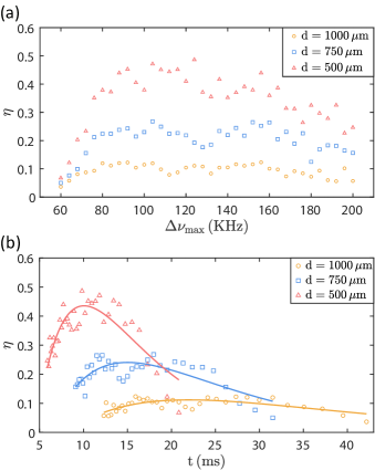
For future PAC experiments, a high density of atoms on the surface of the GaN-on-sapphire chip is desired. Therefore, we experimentally varied the location of the MOT center, and optimized the for atom transportation. The results for maximum transport distance , , and are summarized in Fig. 4, with the atomic density on the chip surface calculated from the fitting results, as shown by the solid line of Fig. 3(a). The transport efficiency is defined as the ratio of the maximum atomic density on the chip surface to the initial atomic density in the standing wave dipole trap. Comparing the different in Fig. 4(a), the transport efficiency reaches the optimum when is , and the transport efficiency drops when is further increased. In particular, the efficiency dramatically decreases when is less than . The dependence of on might be attributed to two different reasons. If is too large, the acceleration and deceleration process of the conveyor belt might induce a significant loss of atoms. Such phenomena have been studied in many other experimental works in detail Schrader et al. (2001); Hickman and Saffman (2020). In contrast, if is too small, the required is too large, and the atomic density is limited by the intrinsic atomic losses in the dipole trap. In practical cases, we aim to obtain higher transport efficiency along with less transport time. In Fig. 4(b), we present the transport efficiency with corresponding transport time for different transport parameter. Shortening the transport distance can improve both the transport efficiency and transport time, and a maximum transport efficiency close to is achieved for a maximum transport distance of . We fit our results with an empirical equation of the form
| (4) |
to describe the relation between transport efficiency with corresponding transport time. The exponential decay accounts for the intrinsic loss irrelevant to the transport velocity, while the linear term accounts for the improvement of transport efficiency with slow transport velocity. It is anticipated that the transport efficiency can be improved by reducing the transport distance. However, the disturbing of the MOT when it is in the proximity of the chip surface prevent us from achieving a shorter distance.
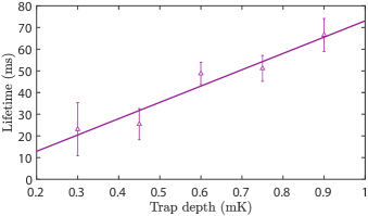
We also notice that the maximum transport efficiency is currently limited to about . While nearly lossless atom transport was achieved for a transport distance of a few milimeters in free space Schrader et al. (2001), the reflection of the dipole trap beams on the chip surface may destroy the moving lattice antinodes in our cases. This issue might be mitigated by choosing an appropriate polarization of the dipole trap beams with incident angle satisfying the Brewster angle, since the reflection can be greatly suppressed. Finally, the intrinsic heating of atoms in the conveyor belt is tested in a static standing wave dipole trap (). As shown in Fig. 5, a heating rate of is extracted from the measurement of the trap lifetime for different trap depths, which explains the severe atomic loss when .
IV Conclusion
We have demonstrated a hybrid photonic-atomic chip platform and successfully transported an ensemble of cold atoms from free space towards the chip with an optical conveyor belt. Our PAC platform is made of transparent materials, allowing full optical access for free space laser cooling, atom transport, and efficient coupling to on-chip photonic waveguides. The maximum transport efficiency of atoms is about with a transport distance of . In the future, by combining on-chip MOT laser cooling, optical transport and evanescent-field trapping of cold atoms, a more compact PAC platform is attainable through the implementation of advanced photonic structure fabrication and design strategies. Our PAC platform holds great potential for studies of atom-photon interactions and the realization of single-photon-level optical nonlinearity, which could find applications in quantum information science and quantum sensing.
V Acknowledgments
This work was funded by the National Key R&D Program (Grant No. 2021YFF0603701), the National Natural Science Foundation of China (Grants No. U21A20433, No. U21A6006, No. 92265210, No. 12104441, No. 12134014, No. 61905234, and No. 11974335), and the USTC Research Funds of the Double First-Class Initiative (Grant No. YD2030002007). CLZ was also supported by the Fundamental Research Funds for the Central Universities, and USTC Research Funds of the Double First-Class Initiative. This work was partially carried out at the USTC Center for Micro and Nanoscale Research and Fabrication.
References
- Chang et al. (2018) D. E. Chang, J. S. Douglas, A. González-Tudela, C.-L. Hung, and H. J. Kimble, “Colloquium : Quantum matter built from nanoscopic lattices of atoms and photons,” Reviews of Modern Physics 90, 031002 (2018).
- Luan et al. (2020) X. Luan, J.-B. Béguin, A. P. Burgers, Z. Qin, S.-P. Yu, and H. J. Kimble, “The integration of photonic crystal waveguides with atom arrays in optical tweezers,” Advanced Quantum Technologies 3, 2000008 (2020).
- Béguin et al. (2020) J.-B. Béguin, A. P. Burgers, X. Luan, Z. Qin, S. P. Yu, and H. J. Kimble, “Advanced apparatus for the integration of nanophotonics and cold atoms,” Optica 7, 1 (2020).
- Wang et al. (2022) W. Wang, Y. Xu, and Z. Chai, “On-chip light-atom interactions: Physics and applications,” Advanced Photonics Research 3, 2200153 (2022).
- Bouscal et al. (2023) A. Bouscal, M. Kemiche, S. Mahapatra, N. Fayard, J. Berroir, T. Ray, J.-J. Greffet, F. Raineri, A. Levenson, K. Bencheikh, C. Sauvan, A. Urvoy, and J. Laurat, “Systematic design of a robust half-W1 photonic crystal waveguide for interfacing slow light and trapped cold atoms,” arXiv , 2301.04675 (2023).
- Lvovsky et al. (2009) A. I. Lvovsky, B. C. Sanders, and W. Tittel, “Optical quantum memory,” Nature Photonics 3, 706 (2009).
- Gouraud et al. (2015) B. Gouraud, D. Maxein, A. Nicolas, O. Morin, and J. Laurat, “Demonstration of a memory for tightly guided light in an optical nanofiber,” Physical Review Letters 114, 180503 (2015).
- Pichler et al. (2017) H. Pichler, S. Choi, P. Zoller, and M. D. Lukin, “Universal photonic quantum computation via time-delayed feedback,” Proceedings of the National Academy of Sciences of the United States of America 114, 11362 (2017).
- Scheucher et al. (2016) M. Scheucher, A. Hilico, E. Will, J. Volz, and A. Rauschenbeutel, “Quantum optical circulator controlled by a single chirally coupled atom,” Science 354, 1577 (2016).
- Lodahl et al. (2017) P. Lodahl, S. Mahmoodian, S. Stobbe, A. Rauschenbeutel, P. Schneeweiss, J. Volz, H. Pichler, and P. Zoller, “Chiral quantum optics,” Nature 541, 473 (2017).
- Kimble (2008) H. J. Kimble, “The quantum internet,” Nature 453, 1023 (2008).
- Tiecke et al. (2014) T. Tiecke, J. D. Thompson, N. P. de Leon, L. Liu, V. Vuletić, and M. D. Lukin, “Nanophotonic quantum phase switch with a single atom,” Nature 508, 241 (2014).
- Muralidharan et al. (2017) S. Muralidharan, C.-L. Zou, L. Li, J. Wen, and L. Jiang, “Overcoming erasure errors with multilevel systems,” New Journal of Physics 19, 013026 (2017).
- Stehle et al. (2014) C. Stehle, C. Zimmermann, and S. Slama, “Cooperative coupling of ultracold atoms and surface plasmons,” Nature Physics 10, 937 (2014).
- Stehle et al. (2011) C. Stehle, H. Bender, C. Zimmermann, D. Kern, M. Fleischer, and S. Slama, “Plasmonically tailored micropotentials for ultracold atoms,” Nature Photonics 5, 494 (2011).
- Douglas et al. (2015) J. S. Douglas, H. Habibian, C.-L. Hung, A. V. Gorshkov, H. J. Kimble, and D. E. Chang, “Quantum many-body models with cold atoms coupled to photonic crystals,” Nature Photonics 9, 326 (2015).
- González-Tudela et al. (2015) A. González-Tudela, C.-L. Hung, D. E. Chang, J. I. Cirac, and H. J. Kimble, “Subwavelength vacuum lattices and atom-atom interactions in two-dimensional photonic crystals,” Nature Photonics 9, 320 (2015).
- Zektzer et al. (2021) R. Zektzer, N. Mazurski, Y. Barash, and U. Levy, “Nanoscale atomic suspended waveguides for improved vapour coherence times and optical frequency referencing,” Nature Photonics 15, 772 (2021).
- Sebbag et al. (2020) Y. Sebbag, A. Naiman, E. Talker, Y. Barash, and U. Levy, “Chip-scale integration of nanophotonic-atomic magnetic sensors,” ACS Photonics 8, 142 (2020).
- Lin et al. (2004) Y.-j. Lin, I. Teper, C. Chin, and V. Vuletić, “Impact of the casimir-polder potential and johnson noise on bose-einstein condensate stability near surfaces,” Phys. Rev. Lett. 92, 050404 (2004).
- Fortágh et al. (2002) J. Fortágh, H. Ott, S. Kraft, A. Günther, and C. Zimmermann, “Surface effects in magnetic microtraps,” Phys. Rev. A 66, 041604 (2002).
- Burgers et al. (2019) A. P. Burgers, L. S. Peng, J. A. Muniz, A. C. McClung, M. J. Martin, and H. J. Kimble, “Clocked atom delivery to a photonic crystal waveguide,” Proceedings of the National Academy of Sciences 116, 456 (2019).
- Thompson et al. (2013) J. D. Thompson, T. Tiecke, N. P. de Leon, J. Feist, A. Akimov, M. Gullans, A. S. Zibrov, V. Vuletić, and M. D. Lukin, “Coupling a single trapped atom to a nanoscale optical cavity,” Science 340, 1202 (2013).
- Samutpraphoot et al. (2020) P. Samutpraphoot, T. Đorđević, P. L. Ocola, H. Bernien, C. Senko, V. Vuletić, and M. D. Lukin, “Strong coupling of two individually controlled atoms via a nanophotonic cavity,” Physical Review Letters 124, 063602 (2020).
- Ðorđević et al. (2021) T. Ðorđević, P. Samutpraphoot, P. L. Ocola, H. Bernien, B. Grinkemeyer, I. Dimitrova, V. Vuletić, and M. D. Lukin, “Entanglement transport and a nanophotonic interface for atoms in optical tweezers,” Science 373, 1511 (2021).
- Kim et al. (2019) M. E. Kim, T.-H. Chang, B. M. Fields, C.-A. Chen, and C.-L. Hung, “Trapping single atoms on a nanophotonic circuit with configurable tweezer lattices,” Nature Communications 10, 1 (2019).
- Zhou et al. (2023) X. Zhou, H. Tamura, T.-H. Chang, and C.-L. Hung, “Coupling single atoms to a nanophotonic whispering-gallery-mode resonator via optical guiding,” Physical Review Letters 130, 103601 (2023).
- Aoki et al. (2006) T. Aoki, B. Dayan, E. Wilcut, W. P. Bowen, A. S. Parkins, T. Kippenberg, K. Vahala, and H. Kimble, “Observation of strong coupling between one atom and a monolithic microresonator,” Nature 443, 671 (2006).
- Will et al. (2021) E. Will, L. Masters, A. Rauschenbeutel, M. Scheucher, and J. Volz, “Coupling a single trapped atom to a whispering-gallery-mode microresonator,” Physical Review Letters 126, 233602 (2021).
- Vetsch et al. (2010) E. Vetsch, D. Reitz, G. Sagué, R. Schmidt, S. Dawkins, and A. Rauschenbeutel, “Optical interface created by laser-cooled atoms trapped in the evanescent field surrounding an optical nanofiber,” Physical Review Letters 104, 203603 (2010).
- Goban et al. (2012) A. Goban, K. Choi, D. Alton, D. Ding, C. Lacroûte, M. Pototschnig, T. Thiele, N. Stern, and H. Kimble, “Demonstration of a state-insensitive, compensated nanofiber trap,” Physical Review Letters 109, 033603 (2012).
- Corzo et al. (2019) N. V. Corzo, J. Raskop, A. Chandra, A. S. Sheremet, B. Gouraud, and J. Laurat, “Waveguide-coupled single collective excitation of atomic arrays,” Nature 566, 359 (2019).
- Reitz et al. (2013) D. Reitz, C. Sayrin, R. Mitsch, P. Schneeweiss, and A. Rauschenbeutel, “Coherence properties of nanofiber-trapped cesium atoms,” Physical Review Letters 110, 243603 (2013).
- Hümmer et al. (2019) D. Hümmer, P. Schneeweiss, A. Rauschenbeutel, and O. Romero-Isart, “Heating in nanophotonic traps for cold atoms,” Physical Review X 9, 041034 (2019).
- Shomroni et al. (2014) I. Shomroni, S. Rosenblum, Y. Lovsky, O. Bechler, G. Guendelman, and B. Dayan, “All-optical routing of single photons by a one-atom switch controlled by a single photon,” Science 345, 903 (2014).
- Barnett et al. (2000) A. H. Barnett, S. P. Smith, M. Olshanii, K. S. Johnson, A. W. Adams, and M. Prentiss, “Substrate-based atom waveguide using guided two-color evanescent light fields,” Physical Review A 61, 023608 (2000).
- Chang et al. (2019) T.-H. Chang, B. M. Fields, M. E. Kim, and C.-L. Hung, “Microring resonators on a suspended membrane circuit for atom–light interactions,” Optica 6, 1203 (2019).
- Liu et al. (2022a) A. Liu, L. Xu, X.-B. Xu, G.-J. Chen, P. Zhang, G.-Y. Xiang, G.-C. Guo, Q. Wang, and C.-L. Zou, “Proposal for low-power atom trapping on a GaN-on-sapphire chip,” Physical Review A 106, 033104 (2022a).
- Liu et al. (2022b) A. Liu, J. Liu, W. Peng, X.-B. Xu, G.-J. Chen, X. Ren, Q. Wang, and C.-L. Zou, “Multigrating design for integrated single-atom trapping, manipulation, and readout,” Physical Review A 105, 053520 (2022b).
- Meng et al. (2015) Y. Meng, J. Lee, M. Dagenais, and S. Rolston, “A nanowaveguide platform for collective atom-light interaction,” Applied Physics Letters 107, 091110 (2015).
- Chen et al. (2022) L. Chen, C.-J. Huang, X.-B. Xu, Y.-C. Zhang, D.-Q. Ma, Z.-T. Lu, Z.-B. Wang, G.-J. Chen, J.-Z. Zhang, H. X. Tang, C.-H. Dong, W. Liu, G.-Y. Xiang, G.-C. Guo, and C.-L. Zou, “Planar-Integrated Magneto-Optical Trap,” Physical Review Applied 17, 034031 (2022).
- Kuhr et al. (2001) S. Kuhr, W. Alt, D. Schrader, M. Muller, V. Gomer, and D. Meschede, “Deterministic delivery of a single atom,” Science 293, 278 (2001).
- Nussmann et al. (2005) S. Nussmann, M. Hijlkema, B. Weber, F. Rohde, G. Rempe, and A. Kuhn, “Submicron positioning of single atoms in a microcavity,” Physical Review Letters 95, 173602 (2005).
- Dinardo and Anderson (2016) B. A. Dinardo and D. Z. Anderson, “A technique for individual atom delivery into a crossed vortex bottle beam trap using a dynamic 1d optical lattice,” Review of Scientific Instruments 87, 123108 (2016).
- Liu et al. (2022c) J. Liu, F. Bo, L. Chang, C.-H. Dong, X. Ou, B. Regan, X. Shen, Q. Song, B. Yao, W. Zhang, C.-L. Zou, and Y.-F. Xiao, “Emerging material platforms for integrated microcavity photonics,” Science China Physics, Mechanics & Astronomy 65, 104201 (2022c).
- Yu et al. (1997) G. Yu, G. Wang, H. Ishikawa, M. Umeno, T. Soga, T. Egawa, J. Watanabe, and T. Jimbo, “Optical properties of wurtzite structure gan on sapphire around fundamental absorption edge (0.78–4.77 ev) by spectroscopic ellipsometry and the optical transmission method,” Applied Physics Letters 70, 3209 (1997).
- Muth et al. (1999) J. Muth, J. D. Brown, M. Johnson, Z. Yu, R. Kolbas, J. Cook, and J. Schetzina, “Absorption coefficient and refractive index of gan, aln and algan alloys,” Materials Research Society Internet Journal of Nitride Semiconductor Research 4, 502 (1999).
- Metcalf and van der Straten (1999) H. J. Metcalf and P. van der Straten, Laser Cooling and Trapping, Graduate Texts in Contemporary Physics (Springer New York, New York, NY, 1999).
- Ketterle et al. (1999) W. Ketterle, D. S. Durfee, and D. Stamper-Kurn, “Making, probing and understanding bose-einstein condensates,” arXiv preprint cond-mat/9904034 (1999).
- Huet et al. (2012) L. Huet, M. Ammar, E. Morvan, N. Sarazin, J.-P. Pocholle, J. Reichel, C. Guerlin, and S. Schwartz, “Experimental investigation of transparent silicon carbide for atom chips,” Applied Physics Letters 100, 121114 (2012).
- Schrader et al. (2001) D. Schrader, S. Kuhr, W. Alt, M. Muller, V. Gomer, and D. Meschede, “An optical conveyor belt for single neutral atoms,” Applied Physics B 73, 819 (2001).
- Hickman and Saffman (2020) G. T. Hickman and M. Saffman, “Speed, retention loss, and motional heating of atoms in an optical conveyor belt,” Physical Review A 101, 063411 (2020).