Venice: Improving Solid-State Drive Parallelism
at Low Cost via Conflict-Free Accesses
Abstract.
The performance and capacity of solid-state drives (SSDs) are continuously improving to meet the increasing demands of modern data-intensive applications. Unfortunately, communication between the SSD controller and memory chips (e.g., 2D/3D NAND flash chips) is a critical performance bottleneck for many applications. SSDs use a multi-channel shared bus architecture where multiple memory chips connected to the same channel communicate to the SSD controller with only one path. As a result, path conflicts often occur during the servicing of multiple I/O requests, which significantly limits SSD parallelism. It is critical to handle path conflicts well to improve SSD parallelism and performance.
Our goal is to fundamentally tackle the path conflict problem by increasing the number of paths between the SSD controller and memory chips at low cost. To this end, we build on the idea of using an interconnection network to increase the path diversity between the SSD controller and memory chips. We propose Venice, a new mechanism that introduces a low-cost interconnection network between the SSD controller and memory chips and utilizes the path diversity to intelligently resolve path conflicts. Venice employs three key techniques: 1) a simple router chip added next to each memory chip without modifying the memory chip design, 2) a path reservation technique that reserves a path from the SSD controller to the target memory chip before initiating a transfer, and 3) a fully-adaptive routing algorithm that effectively utilizes the path diversity to resolve path conflicts. Our experimental results show that Venice 1) improves performance by an average of 2.65/1.67 over a baseline performance-optimized/cost-optimized SSD design across a wide range of workloads, 2) reduces energy consumption by an average of 61% compared to a baseline performance-optimized SSD design. Venice’s benefits come at a relatively low area overhead.
1. Introduction
Flash-memory-based solid-state drives (SSDs) are ubiquitous, from cloud environments to mobile devices (dirik-isca-2009, ; do2013query, ; chen2011hystor, ; stefanov2013oblivistore, ; micheloni2010inside, ; agrawal2008design, ; tavakkol2014design, ; eshghi2018ssd, ; hu2012exploring, ; cho2015design, ; gao2014exploiting, ; gao2017exploiting, ; kim2018autossd, ; tavakkol2016performance, ; kim2022networked, ; lim2010faster, ; kim2019practical, ; cho2013active, ; cai-errors-2018, ; cai2015data, ; cai2013threshold, ; cai2017error, ; tavakkol2018flin, ; park2022flash, ; mutlu-emergingcomputing-2021, ; kim2020evanesco, ; cai2017vulnerabilities, ; cai2012error, ). The high performance, low power consumption and shock resistance of SSDs make them suitable replacements for hard disk drives (HDDs) (dirik-isca-2009, ; kryder2009after, ; mielke2017reliability, ). The rise in the number of data-intensive applications has resulted in the widespread adoption of SSDs in computing systems, increasing the demand for higher performance and capacity in SSDs. Although SSD vendors have significantly improved both performance and capacity of SSDs (e.g., (znand, ; NVMExpress:2014, ; micron3dxpoint, ; shibata20191, ; cai2017error, )) over the years, communication within the SSD (i.e., between the SSD controller and NAND flash chips) is still a critical performance bottleneck (grupp2012bleak, ; nishtala2015high, ; hsu2015nand, ; tavakkol2012network, ; tavakkol2014design, ; park2022flash, ; jung2012evaluation, ; jung2012physically, ; hu2011performance, ; park2010exploiting, ; mao2017improving, ; ruan2012improving, ; gao2019parallel, ; choi2018parallelizing, ) for many applications, especially workloads with a large number of random I/O requests (min2012sfs, ; han2019wal, ; kim2022networked, ; tavakkol2014design, ; tavakkol2012network, ; zhou2015efficient, ; choi2018parallelizing, ; kim2019practical, ; agrawal2008design, ; kim2015improving, ).
Commodity SSDs use a multi-channel shared bus architecture (e.g., (agrawal2008design, ; tavakkol2014design, ; dirik-isca-2009, ; eshghi2018ssd, ; hu2012exploring, ; cho2015design, ; gao2014exploiting, ; gao2017exploiting, ; kim2018autossd, ; tavakkol2016performance, ; kim2022networked, )) for communication between the SSD controller and NAND flash chips. In this architecture, the SSD controller is connected to flash chips via multiple channels (typically 4 to 16 (samsung-ssd-980, ; skhynix-gold-p31, ; microchip-16-channel-controller, )) with a number of flash chips (typically 4 to 32 (samsung-ssd-980, ; skhynix-gold-p31, ; lee2022mqsim, ; pm9a3, )) connected to each channel. Thus, each flash chip has only one path to communicate with the SSD controller and several flash chips share the same path. As a result, there is a high likelihood that multiple I/O requests access NAND flash chips on the same channel. These I/O requests should be transferred serially on the same channel, which significantly limits SSD parallelism. We call this problem path conflict. To quantify the effect of path conflicts on SSD performance, we compare the performance of a state-of-the-art baseline SSD with an ideal (i.e., path-conflict-free) SSD. We observe that the ideal SSD outperforms the baseline SSD by 4 on average across nineteen data-intensive real-world workloads (see §3 for more detail).
SSD vendors attempt to reduce path conflicts by increasing the number of channels in the SSD. However, this is not a scalable solution since increasing the number of channels makes the SSD controller more complex (e.g., the SSD controller needs more I/O pins to service more parallel channels), increasing the overall cost of the SSD. A recent prior work (kim2022networked, ) attempts to address the path conflict problem by increasing the bandwidth of each SSD channel. This work proposes to utilize the control and data pins of flash chips for both command and data transfer, effectively providing 2 the SSD channel bandwidth. Unfortunately, such techniques 1) are expensive as they require relatively large modifications to the commodity NAND flash memory chips (e.g., 20% area overhead in each flash die (kim2022networked, )), and 2) alleviate but cannot effectively resolve path conflicts (as we show in §3.3).
Our goal is to fundamentally address the path conflict problem in SSDs by providing high path diversity at low cost for communication between the SSD controller and flash chips. Our key idea is to use a low-cost interconnection network to increase the path diversity between the SSD controller and flash chips. Some prior works propose the use of an interconnection network within an SSD to provide a scalable solution to increase SSD capacity (tavakkol2014design, ; tavakkol2012network, ). Such works can potentially be repurposed to tackle the path conflict problem. However, prior SSD interconnection network designs have two main weaknesses, which prevent them from effectively addressing the path conflict problem. First, prior works impose significant area (i.e., cost) overhead as they integrate a buffered router (e.g., 16KB buffer per router port) inside each flash chip. Such a design increases the area and the number of I/O pins of the flash chip. Second, prior works do not resolve path conflicts effectively because they employ a simple deterministic routing algorithm, which cannot utilize the interconnection network’s rich path diversity (as we show in §3.3).
We propose Venice,111Named after the network of canals in the city of Venice (venice, ). a new mechanism that introduces a low-cost interconnection network of flash chips to fundamentally tackle the path conflict problem while effectively addressing the two major weaknesses of prior works on SSD interconnection networks. Venice employs three key techniques. First, Venice adds a new router chip next to each flash chip without modifying the flash chip. Routers are connected in a network topology, such as a 2D mesh. Second, Venice reserves a network path for each I/O request before initiating the command and data transfer. This technique ensures that the I/O request transfer does not experience path conflicts in the network, which avoids the need for large buffers in each router. Third, to find a free path between the SSD controller and the flash chip, Venice uses a non-minimal fully-adaptive routing algorithm that effectively utilizes the interconnection network’s path diversity.
We evaluate Venice using MQSim (tavakkol2018mqsim, ; mqsim-github, ), a state-of-the-art SSD simulator. We use two baseline SSD configurations, performance-optimized and cost-optimized and a wide variety of I/O-intensive benchmarks (see §5). Our evaluation yields three key results that demonstrate Venice’s effectiveness. First, for the performance-optimized configuration, Venice improves performance by an average of 2.65 (up to 7.10) and 1.92 (up to 4.30) compared to the baseline SSD design and best-performing prior work (tavakkol2012network, ) (without taking the overhead of prior work into account), respectively. For the cost-optimized configuration, Venice improves performance by an average of 1.67 (up to 3.68) and 1.47 (up to 2.90) compared to the baseline SSD design and the best-performing prior work (tavakkol2012network, ), respectively. Second, Venice reduces energy consumption by an average of 61% and 46% compared to the baseline performance-optimized SSD design and the best-performing prior work (tavakkol2012network, ), respectively. Third, Venice’s benefits come at a relatively low area overhead. Venice’s routers impose 8% area overhead to the SSD printed circuit board (PCB). Venice’s interconnection network links, in total, occupy 44% lower area compared to the baseline multi-channel shared bus architecture.
This paper makes the following contributions:
-
•
We demonstrate the importance of the path conflict problem in modern SSD designs, and quantify its performance impact.
-
•
We propose Venice, a new mechanism that introduces a low-cost interconnection network of flash chips to fundamentally address the path conflict problem in SSDs.
-
•
We introduce three key techniques that enable Venice: 1) a simple router chip added next to each flash chip without modifying the flash chip itself, 2) a path reservation technique to reserve paths from the SSD controller to target flash chips, and 3) a non-minimal fully-adaptive routing algorithm to effectively utilize the path diversity in the interconnection network.
-
•
We rigorously evaluate Venice and show that it significantly improves performance over state-of-the-art SSD designs on both performance- and cost-optimized SSD configurations.
2. Background
We provide a brief background on the baseline multi-channel shared bus SSD architecture. A typical modern SSD consists of an SSD controller and an array of flash chips. The host system uses a high-speed communication interface (e.g., PCIe (pcie-spec, )) to communicate with the SSD. The SSD controller communicates with the flash chips using the shared flash channels. Figure 1 shows a high-level overview of a modern SSD.
2.1. Flash Chip Array
Multiple flash chips ( ) (cai2017error, ; agrawal2008design, ) are connected to a flash controller ( ) through a shared channel in the multi-channel shared bus architecture. Each flash chip ( ) contains one or more (typically 1 to 4) flash dies. Flash dies operate independently of each other. Each die ( ) consists of multiple (e.g., 2 or 4) planes. A plane ( ) typically contains thousands of blocks, and each block ( ) consists of tens to hundreds of pages. A flash page ( ) consists of a set of flash cells connected to the same wordline within a flash block. Read and write operations are typically performed at the granularity of a flash page (e.g., 16KB in size). However, erase operations happen at block granularity (cai-errors-2018, ; cai2015data, ; cai2013threshold, ; cai2017error, ; park2022flash, ; cai2017vulnerabilities, ; cai2012error, ). Planes in the same die share the peripheral circuitry used to access pages; as such, they can concurrently operate only when accessing pages (or blocks) at the same offset, which are called multi-plane operations.
Based on the number of bits stored in a flash cell, it is categorized as a single-level cell (SLC; 1 bit) (cho2001dual, ), multi-level cell (MLC; 2 bits) (lee20043, ), triple-level cell (TLC; 3 bits) (maejima2018512gb, ), or quad-level cell (QLC; 4 bits) (cho20221, ). The capacity of the SSD increases as the flash cell stores more bits, but the increased flash cell density leads to higher latency and lower endurance (grupp2012bleak, ; dirik-isca-2009, ; mohan2010learned, ; boboila2010write, ; cai2017vulnerabilities, ; cai2017error, ; micheloni2010inside, ; mielke2017reliability, ; cai2012error, ; jimenez2014wear, ; margaglia2015improving, ; cai-errors-2018, ).
2.2. SSD Controller
The SSD controller ( ) is responsible for managing the NAND flash chips ( ) and the I/O requests sent by the host ( ). The SSD controller contains an embedded microprocessor that executes firmware called the Flash Translation Layer (FTL) ( ) (gupta2009dftl, ; tavakkol2018mqsim, ; lim2010faster, ; shin2009ftl, ; zhou2015efficient, ). The SSD controller stores metadata (e.g., a logical-to-physical page mapping table) used to manage the FTL functionality and caches frequently accessed pages in DRAM ( ) that is part of the SSD. The SSD controller consists of multiple flash controllers ( ). A flash controller is an embedded processor that interfaces with multiple flash chips using a shared channel. The flash controller selects the flash chip for a read/write operation and initiates the command and data transfer.
Host Interface Layer. Host Interface Layer (HIL) ( ) (jung2019design, ; jung2014hios, ; tavakkol2018mqsim, ) is the interface between the host system ( ) and the SSD controller ( ). HIL communicates with the host system using a communication protocol over the system I/O bus. HIL in a commodity SSD typically supports the Advanced Host Controller Interface (AHCI) (ahci, ) or the NVM Express (NVMe) (NVMExpress:2014, ) interface. AHCI builds upon the Serial ATA (SATA) (sata-spec, ) protocol, which is commonly used to connect the host system to the hard disk drives. AHCI and SATA interfaces provide very low throughput for SSDs because of the availability of a single I/O queue to submit I/O requests to the SSD.
To overcome the throughput bottleneck of AHCI and SATA, modern SSDs have adopted the NVMe protocol, which uses the PCI Express (PCIe) system bus to communicate with the host (see, e.g., (IntelP45002017, ; TOSHIBA2016, ; HGSTSN2002017, ; SandDiskSkyhawk2017, ; OCZ2017, ; tavakkol2018flin, ; tavakkol2018mqsim, ; znand, ; pm9a3, ; 980pro, ; 990pro, )). NVMe directly exposes multiple SSD I/O queues to the host, thereby enabling 1) high-bandwidth and low-latency communication between the SSD and the host, 2) more fine-grained control of the I/O request scheduling policy by the SSD controller (tavakkol2018flin, ). The host system transfers I/O requests into a Submission Queue allocated to the application in the HIL. HIL picks an I/O request from the Submission Queue and sends the request to the FTL for processing. After the completion of the I/O request, the HIL updates the Completion Queue to inform the host system.
Flash Translation Layer ( ). FTL has four major responsibilities (gupta2009dftl, ; tavakkol2018mqsim, ; lim2010faster, ; shin2009ftl, ; zhou2015efficient, ). First, for each page of data, FTL manages the mapping of each logical address (i.e., the requested address in the host system’s address space) to a physical address (i.e., the actual location in the physical flash chips where the requested data resides). Before new data is written to a flash page, an entire flash block that contains the target flash page has to be erased. This is called the erase-before-write requirement. Unfortunately, the erase-before-write requirement of NAND flash memory makes in-place writes prohibitively costly in terms of performance, energy consumption, and lifetime (cai2017error, ; kim2020evanesco, ; cai2017vulnerabilities, ; gupta2009dftl, ; cai-errors-2018, ). To overcome this issue, the FTL implements an out-of-place write policy in modern SSDs (cai2017vulnerabilities, ; cai2017error, ; cai-errors-2018, ). Whenever a page of data is written to by the host system to a logical page address, the FTL 1) invalidates the corresponding physical page address where the overwritten data resides, 2) writes the new page data to a different physical page address, and 3) updates the logical-to-physical page mapping metadata of the logical page.
Second, the FTL performs garbage collection (GC) (yang2014garbage, ; cai2017error, ; tavakkol2018mqsim, ; agrawal2008design, ; shahidi2016exploring, ; lee2013preemptible, ; jung2012taking, ; choi2018parallelizing, ; wu2016gcar, ; cai-errors-2018, ; cai2017vulnerabilities, ) to recover the wasted space due to pages invalidated by the out-of-place write policy. During GC, the FTL 1) chooses a victim block with the least number of valid pages, 2) copies all valid pages in the victim block to another block, 3) updates the logical to physical address mapping metadata for pages that have been already copied, and 4) erases the victim block to use this block for future write operations. Third, the FTL implements a wear-leveling technique to distribute the writes evenly across all the flash blocks so that the flash blocks in the SSD wear out in a uniform manner (shin2009ftl, ; lim2010faster, ; zhou2015efficient, ; murugan2011rejuvenator, ; agrawal2008design, ; jimenez2014wear, ). Having a wear-leveling mechanism in FTL is critical for SSD lifetime as the number of times a flash block can be erased and programmed is limited (sun2016exploring, ; cai2017error, ; tan2015cost, ). Fourth, the FTL avoids frequent lookups to the flash memory by caching frequently-accessed data (e.g., the logical-to-physical page mapping table (gupta2009dftl, )) or frequently-requested pages by the host in the DRAM ( ) that is present inside the SSD.
Flash Controller ( ). A flash controller (FC) (kim2021decoupled, ; kim2022networked, ; wu2012reducing, ; micheloni2010inside, ; microchip-16-channel-controller, ) is an embedded processor in an SSD that interfaces with multiple flash chips connected through a shared channel. The FTL communicates with the FC to perform a NAND flash operation. The FC communicates with the flash chips using the control/data and arbitration pins (micheloni2010inside, ; onfi-2022, ). For a write operation, the FC 1) performs data randomization to avoid high bit error rates caused by worst-case data patterns (cai2017error, ; cai2017vulnerabilities, ; cai-errors-2018, ), 2) performs Error-Correcting Code (ECC) encoding to improve reliability and performance (cai2017error, ; cai2017vulnerabilities, ; park2022flash, ; zhao2013ldpc, ; micheloni2010inside, ; tanakamaru2013error, ; park2021reducing, ), 3) sends a write command (with the physical page address), to the target flash chip, and 4) transfers the randomized ECC-encoded write data to the target flash chip. For a read operation, the FC 1) sends a read command to the target flash chip, 2) receives the read data from the flash chip, 3) performs ECC decoding and corrects possible errors in the data (cai2017error, ; cai2017vulnerabilities, ; park2022flash, ; zhao2013ldpc, ; micheloni2010inside, ; tanakamaru2013error, ; park2021reducing, ; cai-errors-2018, ),222The FC retries the read process if ECC decoding fails (park2021reducing, ; cai-errors-2018, ; cai2017vulnerabilities, ; cai2017error, ; shim2019exploiting, ; cui2022improving, ; du2017laldpc, ; micheloni2010inside, ; liu2019soml, ; cai2015data, ; cai2012error, ; cai2013threshold, ). and 4) derandomizes the read data to recover the original data.
3. Motivation
We describe the path conflict problem in a typical multi-channel shared bus SSD architecture (which we call Baseline SSD) and major approaches to mitigate path conflicts.
3.1. The Path Conflict Problem in Modern SSDs
A typical SSD (e.g., (agrawal2008design, ; dirik-isca-2009, ; gao2014exploiting, ; lee2022mqsim, ; pm9a3, ; 980pro, ; 990pro, ; eshghi2018ssd, ; hu2012exploring, ; cho2015design, ; kim2018autossd, ; tavakkol2016performance, )) uses a multi-channel shared bus architecture for communication between the SSD controller and NAND flash chips. The SSD controller is connected to flash chips via a number of shared channels (typically 4 to 16 (samsung-ssd-980, ; skhynix-gold-p31, ; microchip-16-channel-controller, )) with multiple flash chips (typically 4 to 32 (samsung-ssd-980, ; skhynix-gold-p31, ; lee2022mqsim, ; pm9a3, )) connected to each channel. Figure 2(a) shows an example configuration in such a Baseline SSD where there are four shared channels with four flash chips connected to each shared channel. In Baseline SSD, each flash chip has only one channel (or path) to communicate with the SSD controller. Unfortunately, the flash chips connected to the same channel share the same path to the SSD controller. Path sharing causes the path conflict problem, where an I/O request needs to wait for the path to become free, if the path is being used for another I/O request.
To demonstrate the path conflict problem, we show two examples of service timelines of ongoing read I/O requests in Figure 3. For simplicity, the figure shows only three major steps during a read request, the read command (CMD ), the flash read operation (RD Operation ), and read data transfer from the flash chip to the SSD controller (Transfer ).
The first example (Figure 3 top) shows two ongoing read requests to two different flash chips connected to the same channel (i.e., the two requests experience the path conflict problem). Unfortunately, in this case, only the second step ( ), flash read operation, of the two ongoing read requests can be performed in parallel. Other steps ( and ) should be performed one after the other (i.e., serially) because they use the same path, which increases the total service time (the total time taken for processing an I/O request within the SSD) of these two requests. The second example (Figure 3 bottom) shows two ongoing read requests to two flash chips connected to two different channels (i.e., no path conflict problem). This example shows that these two I/O requests can be serviced completely in parallel, which reduces the total service time of the two I/O requests.
To understand how much the path conflict problem can increase the total service time, we use the latency numbers for CMD , RD Operation , and Transfer from a performance-optimized SSD configuration (see §5). In a performance-optimized SSD configuration, CMD, RD Operation, and Transfer take 10s, 3s, and 4s, respectively (znand, ; cheong2018flash, ). The total service time for the two read requests that experience the path conflict problem (as depicted in Figure 3 top) is 11.01s (i.e., ). In contrast, ideally (i.e., without a path conflict, as depicted in Figure 3 bottom), the total service time of the two requests is 7.01s (i.e., ). Thus, in this simple example, the path conflict problem increases the average I/O access latency by 57%, which in turn results in lower SSD throughput. The performance overhead of path conflicts can be even higher when (1) more than two I/O requests experience path conflicts, and (2) the data transfer size of each request is larger (e.g., a multi-plane operation; see §2).
The path conflict problem affects the performance of read requests more than that of write requests (gao2014exploiting, ; gao2017exploiting, ; jung2012physically, ; hu2011performance, ; park2010exploiting, ; hu2012exploring, ). This is because data transfer time for a read request is comparable to or longer than the flash read latency (znand, ; 3Dxpoint, ; inteloptane, ), while the flash write latency (e.g., 100s for a performance-optimized SSD configuration (znand, ; cheong2018flash, )) dominates the total service time of a write request.
We conclude that the path conflict problem can significantly increase the total service time of I/O requests and limit SSD throughput, especially for read-intensive workloads.
3.2. Approaches to Mitigate Path Conflicts
We describe two major prior approaches to address path conflict problem and their limitations. We quantitatively analyze the effectiveness of these approaches at mitigating path conflicts in §3.3.
Increasing Flash Channel Bandwidth. A recent work by Kim et al. (kim2022networked, ) proposes the Packetized SSD (pSSD) (Figure 2(b)), a technique to increase the flash channel bandwidth to 2 the channel bandwidth of the Baseline SSD. This technique 1) utilizes control and data pins of the flash chip to transfer both commands and data, thus increasing the channel bandwidth, and 2) integrates an on-die controller inside each flash chip to enable packetization between the flash controller and the flash chip. While pSSD can reduce the performance overhead of path conflicts by reducing the I/O transfer latency, pSSD imposes significant area overhead (i.e., 20% (kim2022networked, )) in each flash chip.
Increasing Path Diversity. Prior works (kim2022networked, ; tavakkol2014design, ; tavakkol2012network, ) propose techniques to mitigate path conflicts by increasing the number of paths through which the SSD controller can access a flash chip (i.e., these approaches increase path diversity).
Kim et al. (kim2022networked, ) propose the Packetized Network SSD (pnSSD) (Figure 2(c)), a technique that provides two paths to access each flash chip, which reduces the performance overhead of path conflicts. pnSSD introduces an interconnection network similar to the 2D mesh topology (dally2004principles, ), except in each dimension, flash chips are connected using a shared bus. As a result, an NN flash chip array has N horizontal and N vertical channels. In pnSSD, a flash chip can be accessed using either a horizontal channel or a vertical channel.
Tavakkol et al. (tavakkol2012network, ; tavakkol2014design, ) propose Network-on-SSD (NoSSD) (Figure 2(d)), which replaces the multi-channel shared bus architecture with a 2D mesh interconnection network of flash chips. NoSSD significantly increases the path diversity compared to the Baseline SSD and pnSSD. However, NoSSD has two main weaknesses that limit its effectiveness at mitigating the path conflict problem. First, NoSSD imposes significant area and cost overhead due to 1) the integration of a buffered router (e.g., with a 16KB buffer per router port) inside each flash chip, and 2) 4 increase in the number of I/O pins compared to a commodity flash chip. Second, NoSSD does not utilize the path diversity effectively as NoSSD employs simple deterministic routing (i.e., the dimension-order routing algorithm (dally2004principles, )) that cannot adapt to the availability of multiple free paths between the flash controller and target flash chip.
3.3. Effectiveness of Prior Approaches
Methodology. We study the effectiveness of prior approaches at mitigating path conflicts using a state-of-the-art SSD simulator, MQSim (tavakkol2018mqsim, ; mqsim-github, ), across nineteen real-world data-intensive workloads (see §5 for our methodology). To this end, we measure the speedup of pSSD, pnSSD, and NoSSD over the Baseline SSD in a performance-optimized SSD configuration (see §5). We compare the speedup results with the speedup of the ideal (i.e., path-conflict-free) SSD. In the path-conflict-free SSD, we assume that each flash chip has a direct separate channel to communicate with the SSD controller; therefore, no path conflict can happen. An I/O request does not experience path conflicts in the path-conflict-free SSD, but it can still be delayed if the target flash chip is busy.
Performance Results. Figure 4 shows the performance of pSSD, pnSSD, NoSSD and path-conflict-free SSD compared to the Baseline SSD. We make five major observations. First, the path-conflict-free SSD provides an average of 4 (up to 11.74) the performance of the Baseline SSD since it does not suffer from any path conflict. Second, pSSD shows an average performance improvement of 27% over Baseline SSD due to its increased channel bandwidth. Third, pnSSD provides an average performance improvement of 30% over Baseline SSD due to its increased path diversity. Fourth, NoSSD outperforms Baseline SSD by 35% on average due to the significantly increased path diversity provided by the interconnection network of flash chips. Fifth, although NoSSD outperforms pSSD and pnSSD, NoSSD’s speedup is still greatly lower than the path-conflict-free SSD’s speedup (4). The main reason is that NoSSD does not utilize the path diversity effectively.
We conclude that while prior approaches improve the performance of the SSD at a large cost overhead, none of them effectively mitigate the path conflict problem, and a large potential remains between their performance and the performance of an SSD that does not suffer from path conflicts.
3.4. Our Goal
Based on our observations and analyses in §3.1, §3.2 and §3.3, we conclude that 1) the path conflict problem significantly limits the performance of modern SSDs, and 2) none of the prior approaches (i.e., pSSD, pnSSD, and NoSSD) effectively mitigate the path conflict problem even though they come with significant area overheads and cost overheads.
Our goal is to fundamentally address the path conflict problem in SSDs by 1) providing path diversity inside the SSD at low cost, and 2) effectively utilizing the increased path diversity for communication between the SSD controller and flash chips.
4. Venice
Overview. We design Venice, a new mechanism that fundamentally addresses the path conflict problem in modern SSDs. Venice 1) provides rich path diversity between the SSD controller and flash chips by introducing a low-cost interconnection network of flash chips, and 2) utilizes the path diversity to identify and reserve a conflict-free path for an I/O request .Venice’s design is based on three key techniques: (1) a low-cost interconnection network of flash chips in the SSD (§4.1), (2) reservation of a path between the flash controller and the flash chip for each I/O request (§4.2), and (3) a non-minimal fully-adaptive routing algorithm to utilize the path diversity provided by the interconnection network of flash chips (§4.3).
4.1. Low-Cost Interconnection Network of
Flash Chips
We want to provide rich path diversity between the SSD controller and flash chips at low cost. Venice can utilize the rich path diversity to eliminate path conflicts. To this end, we connect the flash chips using a low-cost interconnection network. The key design decision that enables our approach to be low cost is the separation of the router from the flash chip such that the flash chip is not modified.
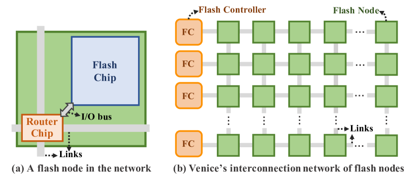
We introduce a new building block, called flash node, which consists of a flash chip and a separate router chip. Figure 5(a) shows a flash node. In each flash node, a flash chip communicates with a router chip using its I/O data pins (i.e., injection/ejection ports) that are otherwise used for connecting the flash chip to the shared channel. Our design connects the flash nodes using an interconnection network topology. Figure 5(b) shows an example interconnection network of flash nodes using the 2D mesh topology. The router chip in each flash node is connected to the router chips in the neighboring flash nodes using bidirectional links.
4.2. Path Reservation
Key Idea. To ensure that the I/O request transfer does not experience path conflicts in the network, Venice reserves a conflict-free path between the flash controller and the target flash chip for each I/O request before starting the transfer. This technique avoids the need for large buffers in each router that are otherwise required to store the data of each I/O request that experiences a path conflict.
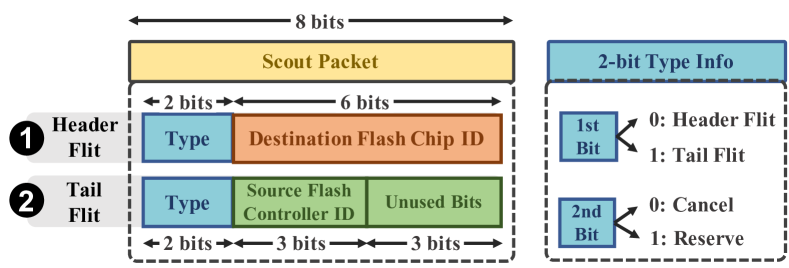
Implementation. Venice identifies and reserves a path by sending a special packet called scout packet. Figure 6 shows the structure of a scout packet for an SSD with 64 flash chips and 8 flash controllers. The scout packet consists of two 8-bit scout flits, a header flit , and a tail flit . Each scout flit contains a 2-bit type information, whose 1) most significant bit denotes whether the flit is the header flit or the tail flit, and 2) least significant bit denotes if the flit is in reserve mode to reserve a link in the path or cancel mode to cancel a reservation. The destination flash chip ID is stored in the last 6 bits of the header flit (6 bits are required to represent 64 flash chips). In the tail flit, 3 bits are used to denote the source flash controller, and the other 3 bits are unused. The source flash controller ID is the same as the scout packet ID.
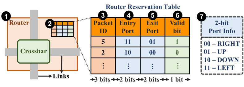
For a given I/O request, Venice checks if the closest flash controller to the target flash chip is available. If so, Venice selects the flash controller to handle the I/O request. Otherwise, Venice uses the nearest free flash controller. The source flash controller sends a scout packet in reserve mode to identify and reserve a path to the destination chip. Venice uses a routing algorithm (e.g., the non-minimal fully-adaptive routing algorithm as described in §4.3) to route a scout packet from the source flash controller to the destination flash chip. Venice reserves the interconnection network’s links that a scout packet takes to reach the destination node. Each reserved link is bidirectional, which enables data transfer 1) from the flash controller to the flash chip (e.g., a write request) using the forward path, and 2) from the flash chip to the flash controller (e.g., a read request) using the backward path. To this end, we introduce a table, called router reservation table, to each router chip. Figure 7 shows the structure of Venice’s router and router reservation table . The router reservation table keeps track of 1) the packet ID , which is the same as the source flash controller ID from which the packet was sent, and 2) which two ports (i.e., entry and exit ports) are connected bidirectionally (based on reservations that were made). Each row in the router reservation table has a valid bit that shows whether the entry is valid. The packet ID has log(n) bits to denote one of the n flash controllers, which allows up to n scout packets to be sent simultaneously. In our example interconnection network configuration with 8 flash controllers, we need 3 bits for the packet ID. The entry port and exit port information in the router reservation table each contains 2 bits to denote one of the four ports in the router.
When the scout packet arrives at the destination flash chip, Venice has already reserved the conflict-free forward and backward paths. The router connected to the destination flash chip uses the backward path to send the scout packet back to the source flash controller. Once the source flash controller receives back the scout packet, it schedules the I/O request transfer using the reserved path.
If a scout packet is unable to find a free link at a router during the path reservation process, the router enables the cancel mode in the scout packet, which cancels the reservation by removing its entry in the router reservation table. The scout packet backtracks along its path to a previously traversed router (i.e., upstream router). Depending on the routing algorithm’s adaptivity, the scout packet may either try a different free output link in the upstream router or backtrack further (i.e., to the upstream router of the upstream router). In case the scout packet is unable to find a free output link during backtracking, the scout packet can arrive back at the flash controller without reserving a path. When the source flash controller receives the scout packet in cancel mode, it retries the path reservation process immediately by sending a new scout packet.333We study more optimizations, including when to resend the scout packet, in the path reservation process in the extended version of our paper (nadig2023venice, ).
4.3. Utilizing Path Diversity
Key Idea. To effectively utilize the interconnection network’s path diversity, Venice uses a non-minimal fully-adaptive routing algorithm for routing a scout packet (during the path reservation process) through the interconnection network of flash nodes. Venice’s non-minimal fully-adaptive routing algorithm dynamically identifies a conflict-free path between the flash controller and the flash chip. This algorithm effectively utilizes the idle links in the interconnection network to find a non-minimal path when a minimal path is unavailable.
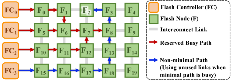
Figure 8 illustrates how a non-minimal fully-adaptive routing algorithm helps to mitigate the path conflict problem via an example. In this example, a new I/O request has as its destination flash chip. In the network, there are three paths already reserved for other I/O requests (marked in red in Figure 8): , , and . The only free flash controller, , is assigned to request . Each minimal path from to has at least one busy link, and thus, is not path-conflict-free. However, there are a number of non-minimal paths from the to that are path-conflict-free. An example is (shown in blue in Figure 8). Venice uses a non-minimal fully-adaptive routing algorithm (described in Algorithm 1) during the path reservation process to increase its ability to mitigate the path conflict problem.
To effectively use a non-minimal fully-adaptive routing algorithm during the path reservation process in Venice, we should address two key challenges: 1) performance overhead of exercising a non-minimal path to service the I/O request, and 2) the need to avoid deadlock/livelock. We describe these two key challenges and Venice’s techniques to address them.
Performance Overhead of Exercising a Non-Minimal Path. The increased path length of the non-minimal route can cause two issues. First, a non-minimal path may lead to an increase in the command/data transfer time and thus the overall latency for servicing the I/O request. After reserving a free path, the transfer latency () in seconds can be calculated using Equation 1:
| (1) |
where distance, , link_width, and are the number of links between the flash controller and flash chip (i.e., hops), the command/data transfer size in terms of the number of bytes, the link width in terms of the number of bytes, and the latency of a single transfer (of size link_width) on the link in seconds, respectively. A non-minimal path has a longer distance compared to a minimal path. We study the latency overhead of a non-minimal path for I/O data and flash command transfer. For the I/O data transfer, the performance overhead of a longer path is negligible. This is because dominates as I/O data transfers are large in size (e.g., 16KB). Flash commands, on the other hand, have a small (i.e., only a few bytes), and thus, a longer path can significantly increase their transfer latency. As discussed in §3.1, the service time of an I/O request consists of flash command transfer time, flash operation latency and I/O data transfer time. The total service time is dominated by the I/O data transfer time and the flash operation latency, and thus, the longer command transfer time due to a non-minimal path has a negligible effect on the total service time of the I/O request.
Second, a non-minimal path occupies more links in the interconnection network compared to a minimal path. If a minimal path is used instead of a non-minimal path, the extra links of a non-minimal path can potentially be used for transferring other ongoing requests, which increases the effectiveness of Venice. To this end, Venice attempts to find path-conflict-free minimal paths during the path reservation process as much as possible (as described in Algorithm 1).
Need to Avoid Deadlock/Livelock. A non-minimal fully-adaptive routing algorithm can potentially cause (1) deadlock in the interconnection network (duato2003interconnection, ; dally2004principles, ; moscibroda2009case, ; gravano1994adaptive, ; fallin2011chipper, ; fallin2012hird, ; glass1992turn, ; fu2011abacus, ; shafiee2011application, ; ebrahimi2017ebda, ; duato1995necessary, ; ausavarungnirun2014design, ), where multiple network packets cannot move forward as they circularly depend on each other to free up resources (e.g., channels, buffers), and (2) livelock (duato2003interconnection, ; dally2004principles, ; moscibroda2009case, ; gravano1994adaptive, ; fallin2011chipper, ; fallin2012hird, ; navaridas2009understanding, ; berman1992adaptive, ; glass1992turn, ; coli1995adaptive, ; ausavarungnirun2014design, ), where at least one packet keeps traversing the network without reaching its destination. Venice’s interconnection network can experience deadlock and livelock only during the path reservation process where the scout packets are routed using the non-minimal fully-adaptive routing algorithm.444Once a path between the flash controller and the destination flash chip is reserved, there is no 1) deadlock, as there is no path conflict during I/O data or flash command transfer, or 2) livelock, as the path from the source flash controller and the destination flash chip is deterministically set as a circuit.
Venice handles deadlock by using backtracking of a scout packet. When a scout packet experiences path conflict during the path reservation process, it backtracks along its path to the previously visited router (i.e., the upstream router) in order to choose a different path. As a result, a scout packet is never blocked due to resource unavailability in the network and deadlock does not happen.
Venice handles livelock by restricting the number of times a scout packet can visit the same router. A scout packet can reserve each output port of a router only once and hence, the scout packet may revisit the same router at most three times555 The number of times a scout packet can revisit a router is four minus one, i.e., number of ports in a router minus the entry port of the scout packet. in an interconnection network with a 2D mesh topology. When a scout packet revisits the same router three times, the scout packet traces its path back to the upstream router (using the router reservation table) and attempts to reserve a different output port in the upstream router. In the worst case, when a scout packet fails to reserve a path to the destination after visiting all the routers at most three times, it will return to the source flash controller. The flash controller immediately sends a new scout packet to retry the path reservation.
Implementation. Algorithm 1 shows the pseudocode for the non-minimal fully-adaptive routing algorithm in Venice. The inputs to the algorithm are: 1) scout packet ID, 2) current router ID, 3) scout packet’s destination router ID, 4) input port of the router through which the scout packet has arrived, 5) the status (free or busy) of the output ports in the router, and 6) the interconnection network structure in terms of number of rows and columns (assuming a 2D mesh topology). The algorithm returns the output port in which the scout packet should traverse to the downstream router.
Input: scout packet ID: , current router ID: , scout packet’s destination router ID: , the Input_port, the output ports’ status, and network structure: rows and columns
Output: Output_port
To find an appropriate output port, the algorithm first attempts to find a free output port that leads to a minimal path (lines 2-32). To this end, the algorithm compares the current router ID with the scout packet’s destination router ID in both X (horizontal) and Y (vertical) dimensions. Based on the comparison, it switches among nine cases (lines 5-26). In each case, the algorithm checks the status of the corresponding output port and adds the output port to the output list if the corresponding output port is free (e.g., lines 6-10).
The algorithm checks the number of output ports added to the output list (line 27). In a 2D mesh topology, the size of the output list can be either two, one, or zero. If there are two output port candidates in the output list, the algorithm randomly selects one output port using a pseudo-random number generator. We use a simple 2-bit Linear-Feedback Shift Register (LFSR) (wang1988linear, ) present in the router for the pseudo-random number generation. The algorithm adds an entry to the router reservation table using the scout packet ID, the input port, and the selected output port. The scout packet then proceeds to the downstream router using the selected output port (lines 27-29). If there is only one output port candidate in the output list, the algorithm selects that output port and records it in the router reservation table (lines 30-32).
However, if the output list is empty, the algorithm has failed to find any free output port that leads to a minimal path. In this case, the algorithm misroutes the scout packet via a free output port that leads to a non-minimal path. To this end, the algorithm randomly selects any free output port (except the ejection port) and adds an entry to the router reservation table (lines 34-45). If the only available free output port is the port that results in backtracking to the upstream router, the scout packet travels back to the upstream router, and the algorithm does not reserve the selected output port (lines 46-47). When the upstream router receives the backtracking scout packet, it clears the reservation entry for the scout packet in the router reservation table and tries another available output port, if any. This algorithm is used in conjunction with the livelock avoidance mechanism of Venice that is described earlier in this section (not shown in Algorithm 1). Note that it is also possible to employ other non-minimal fully-adaptive routing algorithms in Venice instead of this specific one we use and evaluate.
5. Methodology
Simulation Methodology. We evaluate Venice using MQSim (tavakkol2018mqsim, ; mqsim-github, ), a state-of-the-art open-source SSD simulator. MQSim models all components of the SSD, including host interface, SSD controllers, flash controllers, and flash chips. MQSim supports multi-queue SSDs and measures the end-to-end latency (tavakkol2018mqsim, ), which makes it a suitable tool for our study. We model two SSD configurations: 1) a performance-optimized configuration based on Samsung Z-NAND SSD (znand, ; cheong2018flash, ) and 2) a cost-optimized configuration based on Samsung PM9A3 SSD (pm9a3, ). Table 1 provides details of the storage characteristics of the two configurations and Venice’s design parameters used in our evaluation.
| Performance-optimized SSD (znand, ; cheong2018flash, ) | 240GB, Z-NAND (znand, ; cheong2018flash, ; SZ985, ), |
|---|---|
| 8-GB/s External I/O bandwidth (4-lane PCIe Gen4); | |
| 1.2-GB/s Flash Channel I/O rate | |
| NAND Config: 8 channels, 8 chips/channel, | |
| 1 die/chip, 2 planes/die, 128Gb die capacity, | |
| 1024 blocks/plane, 768 pages/block, 4KB page | |
| Latencies: Read(tR): 3s; Erase (tBERS): 1s | |
| Program (tPROG): 100s | |
| Cost-optimized SSD (pm9a3, ) | 1TB, 3D TLC NAND Flash, |
| 8-GB/s External I/O bandwidth (4-lane PCIe Gen4); | |
| 1.2-GB/s Flash Channel I/O rate | |
| NAND Config: 8 channels, 8 chips/channel, | |
| 1 die/chip, 2 planes/die, 1024 blocks/die, 16KB page | |
| Latencies: Read (tR): 45s; Erase (tBERS): 3.5s | |
| Program (tPROG): 650s | |
| Venice Design Parameters | Topology. 88 2D mesh topology, 8-bit 1 GHz links, |
| One router next to each flash chip | |
| Router Architecture. Two 8-bit buffers per port, | |
| 1 GHz frequency | |
| Routing Algorithm. Non-minimal fully-adaptive | |
| Switching. Circuit switching (dally2004principles, ) |
To evaluate Venice’s power overhead, we measure the power consumption of each router and network link in the interconnection network (see §6.6). We analyze 1) the average power consumption of a router by implementing its hardware description language (HDL) model and synthesizing it for the UMC 65nm technology node (umc, ), and 2) the average power consumption for a 4KB data transfer over each network link using the ORION 3.0 (kahng2015orion3, ) power model. To model the power consumption of flash read and write operations, we use the power values from Samsung Z-SSD SZ985 (SZ985, ).
Evaluated Systems. We compare Venice with the following prior approaches (described in §3): (1) Baseline SSD, a typical SSD with multi-channel shared bus architecture; (2) Packetized SSD (pSSD) (kim2022networked, ), a prior proposal that uses packetization to double the flash channel bandwidth; (3) Packetized Network SSD (pnSSD) (kim2022networked, ), a technique that increases path diversity by introducing vertical flash channels; (4) NoSSD (tavakkol2012network, ; tavakkol2014design, ), a state-of-the-art proposal on interconnection network of flash chips that uses a deterministic minimal routing policy to route I/O requests. We compare Venice and the four prior approaches with an ideal path-conflict-free SSD. In a path-conflict-free SSD, we assume that each flash chip has a direct separate channel to communicate with the SSD controller, which eliminates path conflicts.
Workloads. We select nineteen data-intensive storage workloads from MSR Cambridge traces (narayanan2008write, ), Yahoo! Cloud Serving Benchmark (YCSB) suite (cooper2010benchmarking, ), Slacker (harter2016slacker, ), SYSTOR ’17 (lee2017understanding, ) and YCSB RocksDB traces (yadgar2021ssd, ) that are collected from real enterprise and datacenter workloads. These workloads are chosen to represent diverse I/O access patterns, with different read and write ratios, I/O request sizes, and inter-request arrival times. Table 2 reports the characteristics of the workloads chosen for our evaluation.
| Traces | Read % |
|
|
|||||
|---|---|---|---|---|---|---|---|---|
| MSR Cambridge (narayanan2008write, ) | hm_0 | 36 | 8.8 | 58 | ||||
| mds_0 | 12 | 9.6 | 268 | |||||
| proj_3 | 95 | 9.6 | 19 | |||||
| prxy_0 | 3 | 7.2 | 242 | |||||
| rsrch_0 | 9 | 9.6 | 129 | |||||
| src1_0 | 56 | 43.2 | 49 | |||||
| src2_1 | 98 | 59.2 | 50 | |||||
| usr_0 | 40 | 22.8 | 98 | |||||
| wdev_0 | 20 | 9.2 | 162 | |||||
| web_1 | 54 | 29.6 | 67 | |||||
| YCSB (cooper2010benchmarking, ) | YCSB_B | 99 | 65.7 | 13 | ||||
| YCSB_D | 99 | 62 | 14 | |||||
| Slacker (harter2016slacker, ) | jenkins | 94 | 33.4 | 615 | ||||
| postgres | 82 | 13.3 | 382 | |||||
| SYSTOR ’17 (lee2017understanding, ) | LUN0 | 76 | 20.4 | 218 | ||||
| LUN2 | 73 | 16 | 320 | |||||
| LUN3 | 7 | 7.7 | 3127 | |||||
| YCSB RocksDB (yadgar2021ssd, ) | ssd-00 | 91 | 90 | 5 | ||||
| ssd-10 | 99 | 11.5 | 2 |
To evaluate Venice under real-world scenarios, where multiple workloads access the same SSD, we create mixed workloads by combining two or three independent storage workloads. Table 3 shows six mixed workloads and their different characteristics.
Mixed workloads usually have a higher intensity of I/O requests (i.e., lower inter-request arrival time between I/O requests), which likely exacerbates the path conflict problem in the SSD.
| Mix |
|
Description |
|
||||
|---|---|---|---|---|---|---|---|
| mix1 | src2_1 and proj_3 |
|
5.8 | ||||
| mix2 |
|
|
8.4 | ||||
| mix3 | prxy_0 and rsrch_0 |
|
93 | ||||
| mix4 |
|
|
56 | ||||
| mix5 |
|
|
5 | ||||
| mix6 |
|
|
3 |
Metrics. To compare Venice with prior systems, we report the following metrics in our experimental results (see §6) for each workload: 1) performance in terms of speedup in overall execution time over Baseline SSD, 2) SSD throughput in IOPS (i.e., number of I/O operations per second), 3) tail latency in the 99th percentile of I/O requests, 4) SSD power/energy consumption, and 5) power and area overheads.
6. Evaluation
6.1. Performance Analysis
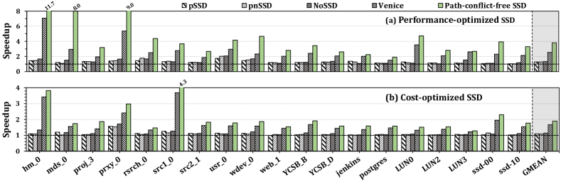
Execution Time. Figures 9(a) and 9(b) show the performance improvement of pSSD, pnSSD, NoSSD, Venice and path-conflict-free SSD over Baseline SSD in terms of speedup in overall execution time of each workload in a performance-optimized SSD and a cost-optimized SSD, respectively.
We make three key observations. First, Venice consistently outperforms all the prior approaches across all workloads in both SSD configurations. In the performance-optimized SSD configuration, Venice outperforms Baseline SSD/pSSD/pnSSD/NoSSD by an average of 2.65/2.10/2.00/1.92 across all workloads. In the cost-optimized SSD configuration, Venice shows an average performance speedup of 1.67/1.52/1.55/1.47 over Baseline SSD/pSSD/pnSSD/NoSSD. Second, Venice results in higher performance improvements in the performance-optimized SSD configuration. This is because the performance-optimized SSD uses fast flash chips (with significantly lower read/write latencies), and thus the I/O data transfer time within the SSD dominates the I/O service time. As a result, improving I/O data transfer performance in the performance-optimized SSD provides a higher improvement in workload execution time. Third, Venice performs within 45% and 25% of the path-conflict-free SSD in the performance-optimized and cost-optimized SSD configuration, respectively. We conclude that Venice significantly improves workload execution time by mitigating the path conflict problem in modern SSDs.
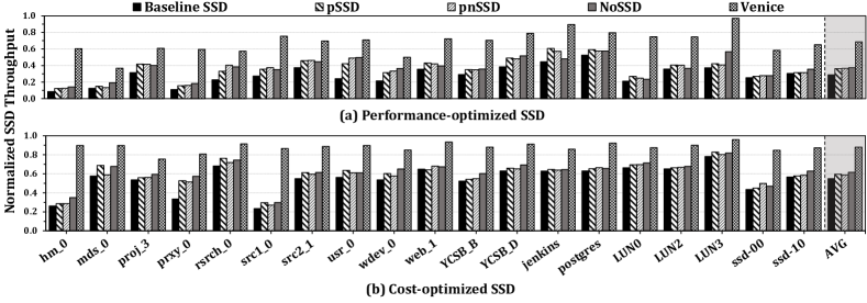
SSD Throughput. Figures 10(a) and 10(b) show the SSD throughput (in IOPS) of Baseline SSD, pSSD, pnSSD, NoSSD and Venice in a performance-optimized SSD and cost-optimized SSD, respectively. We normalize the SSD throughput results to the path-conflict-free SSD’s throughput.
We make two key observations. First, Venice improves SSD throughput over Baseline SSD/pSSD/pnSSD/NoSSD by 176%/120%/113%/102% in the performance-optimized SSD and 76%/58%/61%/51% in the cost-optimized SSD configuration. Second, Venice’s SSD throughput is within 30% and 10% of the path-conflict-free SSD’s throughput in the performance-optimized and cost-optimized SSD configuration, respectively. We conclude that Venice significantly improves SSD throughput by mitigating the path conflict problem.
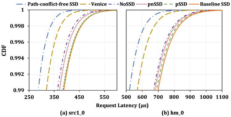
Tail Latency. Path conflicts can cause some I/O requests to experience significantly long access latencies. Figures 11(a) and 11(b) show the 99th percentile of I/O request latencies (i.e., tail latency) in the path-conflict-free SSD, Venice, NoSSD, pnSSD, pSSD and Baseline SSD in the form of a cumulative density function (CDF) for two representative workloads src1_0 and hm_0, respectively. We use only the performance-optimized SSD configuration for this experiment. We make the key observation that Venice significantly reduces the tail latency compared to prior systems. For src1_0, Venice reduces the tail latency by 32%/31%/30%/27% over Baseline SSD/pSSD/pnSSD/NoSSD. For hm_0, Venice reduces the tail latency by 22%/21%/18%/17% over Baseline SSD/pSSD/pnSSD/NoSSD.
6.2. Mixed Workloads
To evaluate the effectiveness of Venice at improving SSD performance in real-world scenarios where multiple workloads access the SSD, we compare SSD performance using different systems under six mixed workloads. Figure 12 shows the speedup of pSSD, pnSSD, NoSSD, Venice and path-conflict-free SSD over Baseline SSD for six mixed workloads. We report results only for the performance-optimized SSD configuration.
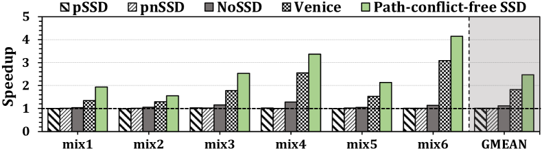
We make two key observations. First, across all mixed workloads, Venice improves performance over prior works. Venice provides an average speedup of 1.83/1.81/1.80/1.63 over Baseline SSD/pSSD/pnSSD/NoSSD. Second, Venice’s performance improvement is higher in mix6. In mix6, the average inter-request arrival time is 90% lower than its constituent workloads, leading to increased path conflicts in Baseline SSD. Venice is able to schedule I/O requests on conflict-free paths using its non-minimal fully-adaptive routing algorithm. We conclude that Venice outperforms prior approaches on high-intensity mixed workloads by effectively mitigating path conflicts.
6.3. Path Conflict Analysis
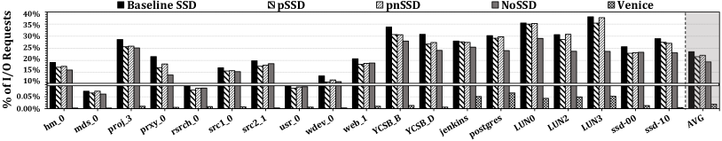
To show the effectiveness of Venice at mitigating the path conflict problem, we measure the percentage of I/O requests in each workload that experience path conflicts using different systems. Figure 13 shows the results for the Baseline SSD, pSSD, pnSSD, NoSSD and Venice in the performance-optimized SSD configuration.
We make the key observation that Venice significantly mitigates the path conflict problem. Our experimental results show that Venice provides conflict-free paths (on the first try) for 99.98% of I/O requests, on average, across all workloads, while Baseline SSD/pSSD/pnSSD/NoSSD provides conflict-free paths for 76.40%/78.47%/77.88%/80.65% of I/O requests. For a small number of I/O requests (i.e., 0.02% of I/O requests, on average), Venice fails to find conflict-free paths on the first try, and thus, the corresponding I/O requests should wait for a longer amount of time until Venice successfully reserves conflict-free paths. Venice’s path reservation process can fail due to two major reasons. First, if all flash controllers are busy processing ongoing I/O requests, Venice cannot start the path reservation process for a new I/O request until a flash controller becomes idle. Second, during the path reservation process, a scout packet (see §4.2) cannot reserve a path if all the links leading to the destination flash chip are reserved. We conclude that Venice effectively eliminates the path conflict problem via path reservation and effective utilization of path diversity in the SSD interconnection network.
6.4. Power and Energy Consumption
We study the impact of Venice and prior approaches on the SSD power and energy consumption.
Average SSD Power Consumption. Figure 14(a) shows the average power consumption for pSSD, pnSSD, NoSSD and Venice on a performance-optimized SSD configuration. Average power consumption values are normalized to the average power consumption of the Baseline SSD.
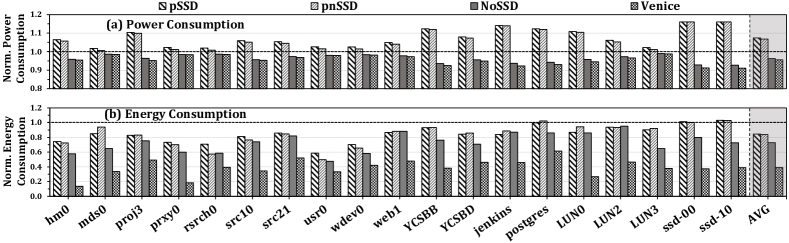
We make four key observations. First, Venice reduces SSD average power consumption by 4% compared to the Baseline SSD. This is mainly because a link in the interconnection network consumes significantly lower power than the shared channel (see §6.6). Second, Venice consumes slightly less power (around 1%) than NoSSD due to Venice’s simple router design. Third, the impact of Venice and prior systems on SSD power consumption is small since the SSD power consumption is dominated by flash operations (i.e., read, program, and erase). The number of flash operations remains the same in Venice and all prior systems.
SSD Energy Consumption. To calculate the energy consumption of Venice and prior approaches, we multiply the average power consumption by the overall execution time of each workload. Figure 14(b) shows the energy consumption for pSSD, pnSSD, NoSSD and Venice on a performance-optimized SSD configuration. Energy consumption values are normalized to the Baseline SSD.
We make the key observation that Venice has significantly lower energy consumption than prior approaches across all workloads. Venice reduces energy consumption by an average of 61%/54%/53%/46% compared to Baseline SSD/pSSD/pnSSD/NoSSD. We conclude that Venice’s lower average power consumption and lower execution time together result in largely lower energy consumption compared to prior systems.
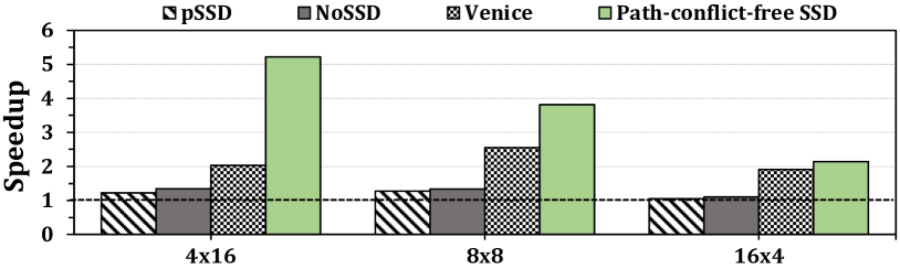
6.5. Sensitivity to Interconnection Network Configurations
We study the effect of the interconnection network configuration on Venice’s performance improvement. To this end, we compare the performance of Venice and prior works using three systems that use 4, 8, and 16 flash controllers in the performance-optimized SSD configuration. We keep the total number of flash chips in the SSD constant across the three systems. Figure 15 shows the average speedup of pSSD, NoSSD, Venice, and path-conflict-free SSD over the Baseline SSD, across all workloads. The X-axis shows three systems, 416, 88, and 164. 416, for example, denotes four flash controllers with 16 flash chips in each row of the flash array.666Note that we omit pnSSD from this study because pnSSD requires an NN flash array configuration where N is the number of flash controllers as well as the number of flash chips in each row in the flash array. Hence, 416 and 164 configurations are not supported by pnSSD.
We make two key observations from our sensitivity analysis. First, Venice provides significant speedup over prior approaches across all three systems with different numbers of flash controllers. Venice outperforms Baseline SSD/pSSD/NoSSD by 1) 2/1.7/1.5 in 416, 2) 2.6/2/1.9 in 88, and 3) 1.9/1.8/1.7 in 164. Second, Venice’s performance improvement is higher for the 88 flash array configuration compared to both 416 and 164 configurations. In the system with 4 flash controllers, Venice can reserve conflict-free paths for up to four ongoing I/O requests. Venice can reserve conflict-free paths for up to eight I/O requests in the system with 8 flash controllers. As a result, Venice has a lower ability to eliminate the path conflict problem in the system with 4 flash controllers, which results in lower performance improvements for Venice. On the other hand, the system with 16 flash controllers has a lower number of path conflicts compared to systems with 4 and 8 flash controllers, and thus, Venice provides lower performance improvement compared to those in the other two systems. We conclude that Venice is effective for different SSD interconnection network configurations.
6.6. Power and Area Overhead Analysis
Power. As discussed in §6.4, Venice reduces average power and energy consumption. This section studies the power consumption of Venice’s interconnection network router and links. We analyze the power consumption of the router by implementing its hardware description language (HDL) model and synthesizing it for the UMC 65nm technology node (umc, ). We observe that each router consumes 0.241 mW. We measure the power consumption of each network link using ORION 3.0 (kahng2015orion3, ) power model tool and observe that each link consumes about 1.08 mW for a 4KB NAND flash page transfer, which is 90% less power consumption than that of a shared channel bus. Each network link consumes significantly lower power than a shared channel bus due to its lower capacitance load. Link capacitance is lower than bus capacitance since (1) it is shorter and thinner than a shared bus and (2) it has only two drivers compared to several (e.g., 8 in an 8 flash array configuration) drivers in a shared bus. Table 4 (3rd column) summarizes the power consumption of Venice’s components. We have already observed in §6.4 that Venice reduces the average power consumption by 4% over Baseline SSD.
| Component |
|
|
|
||||
|---|---|---|---|---|---|---|---|
| Router |
|
0.241 |
|
||||
| Link |
|
1.08 |
|
Area. Venice does not impose area overhead on NAND flash chip design as it does not integrate the router inside the NAND flash chip (i.e., no pins are added to the commodity flash chips). Router chips and the links connecting them can impose area overhead on SSD printed circuit board (PCB) design. To estimate this overhead, we model the area overhead of the interconnection network’s routers and links.
We estimate the area overhead of Venice’s routers using the HDL model of the router. Each router in Venice has an area of 614 . However, each router occupies a higher area on the PCB due to its I/O pad overheads. Each router has 40 I/O pins. Considering I/O pad sizes (about 0.2 mm) and the safety distance between two I/O pads (about 0.2 mm), we expect that each router occupies about 8 , which is 8% of a typical 100 NAND flash chip (kang201913, ).
We estimate the area overhead of Venice’s links using ORION 3.0 (kahng2015orion3, ).
Assuming an 88 2D mesh topology connecting 64 NAND flash chips, Venice requires 112 network links (instead of the eight shared channels required in the baseline).
Note that we do not count injection/ejection links as they are the same as flash chips’ connectors to the shared channel bus.
Our experimental results show that each link’s area is roughly 0.04 of the shared channel area. As a result, in total, Venice’s interconnect links occupy 44% lower area compared to the baseline multi-channel shared bus architecture.777 We measure the total area overhead of Venice’s interconnect links compared to a baseline multi-channel shared bus architecture using this equation:
1 - (total area of interconnection network links) / (total area of channels in multi-channel shared bus architecture), i.e., 1 - (#Links ) / (#Channels ) = 1 - (112 0.04) / (8 1) = 0.44.
A network link occupies significantly smaller space than a bus for two main reasons. First, links are shorter than buses (e.g., by 8 in our case); thus, link wires can be 8 thinner to ensure the same impedance as the bus. Second, as the link wires are thinner, they require lower pitch sizes, reducing the overall area required by the links.
We summarize the area overhead of Venice’s components in Table 4 (4th column). We conclude that Venice’s benefits come at relatively low area overhead.
7. Related Work
To our knowledge, Venice is the first work that fundamentally addresses the path conflict problem in SSDs at low cost. We have quantitatively compared Venice extensively to three major prior works, pSSD (kim2022networked, ), pnSSD (kim2022networked, ) and NoSSD (tavakkol2012network, ; tavakkol2014design, ) in §6. In this section, we briefly review related work in two domains: 1) improving flash array parallelism, and 2) exploiting flash array parallelism.
Improving Flash Array Parallelism. Prior works propose to employ an interconnection network inside the SSD (e.g., (kim2022networked, ; tavakkol2012network, ; tavakkol2014design, ; schuetz2007hyperlink, ; gillingham2013800, ; gillingham2011256gb, ; kim2021decoupled, )). HyperLink NAND flash architecture (HLNAND) (schuetz2007hyperlink, ; gillingham2013800, ; gillingham2011256gb, ) connects the flash chips using a ring-topology interconnection network. Decoupled SSD (kim2021decoupled, ) proposes an on-chip router within each flash controller to create a network of flash controllers in the SSD. Unfortunately, both HLNAND and Decoupled SSD do not provide rich path diversity between the flash controllers and flash chips, and thus, cannot effectively mitigate the path conflict problem.
Exploiting Flash Array Parallelism. Other prior works (e.g., (park2010exploiting, ; ruan2012improving, ; jung2012physically, ; mao2017improving, ; gao2019parallel, ; jung2012evaluation, ; gao2014exploiting, ; gao2017exploiting, ; tavakkol2018flin, ; wang2013novel, )) attempt to exploit the internal parallelism in an SSD to improve the SSD performance. These works mainly focus on I/O scheduling. Jung et al. (jung2012physically, ) propose Physically Addressed Queueing (PAQ), an I/O scheduler implemented in a layer between the FTL and the flash array. PAQ selects groups of operations that can be simultaneously executed without contention for a shared resource (e.g., flash channel). Gao et al. (gao2014exploiting, ; gao2017exploiting, ) propose Parallel Issue Queuing (PIQ), a host I/O scheduler that batches I/O requests that use different flash channels to be scheduled simultaneously to exploit SSD-level parallelism. FLIN (tavakkol2018flin, ) provides both high-performance and fair I/O scheduling in modern SSDs. We believe Venice is orthogonal to these works and I/O scheduling for the Venice architecture is an interesting research direction.
Several prior works (hu2011performance, ; hu2012exploring, ; tavakkol2016performance, ; jung2012evaluation, ; chen2011essential, ; xie2018exploiting, ; zhang2019spa, ) propose techniques to exploit flash array parallelism by focusing on physical page allocation in the FTL. Unfortunately, these works fail to effectively lay out data such that SSD does not experience the path conflict problem. This is due to 1) random data access patterns in SSDs, 2) I/O interference from multiple concurrent applications, and 3) dynamic changes in device conditions.
8. Discussion
We propose Venice to improve SSD performance by mitigating the path conflict problem in SSDs. Venice can be extended to improve SSD and system performance in other ways. We discuss other use cases of Venice in this section.
Applicability of Venice to Near-Data Processing (NDP). NDP is a computing paradigm that moves the computation closer to where the data resides (e.g., (seshadri-ieeecal-2015, ; seshadri-micro-2017, ; hajinazar-asplos-2021, ; seshadri-osdi-2014, ; gao-micro-2021, ; mutlu-emergingcomputing-2021, ; park2022flash, ; aga-hpca-2017, ; li-dac-2016, ; mansouri-asplos-2022, ; gu-isca-2016, ; mailthody-micro-2019, ; mutlu2019processing, ; pei-tos-2019, ; truong-micro-2021, ; acharya-asplos-1998, ; koo-micro-2017, ; kang-micro-2021, ; jun-isca-2018, ; ghose2019processing, ; riedel2001active, ; riedel1998active, ; kang2013enabling, ; keeton1998case, ; do2013query, ; kim2016storage, ; torabzadehkashi2019catalina, ; lee2020smartssd, ; ajdari2019cidr, )). Venice’s improved parallelism can facilitate NDP inside the SSD by efficiently co-locating different operands required by the NDP operations. Prior proposals (gao-micro-2021, ; park2022flash, ) that perform in-flash bulk bitwise operations have data location constraints where the operands must be moved to a single flash chip before the computation is performed. Path conflicts can impact this data movement, which can significantly reduce the performance benefits of in-flash processing. Venice can leverage its improved flash-array parallelism to efficiently gather operand data from different flash chips to the target flash chip that performs the NDP computation.
Improving Garbage Collection. The garbage collection (GC) process (yang2014garbage, ; cai2017error, ; tavakkol2018mqsim, ; agrawal2008design, ; shahidi2016exploring, ; lee2013preemptible, ; jung2012taking, ; choi2018parallelizing, ; wu2016gcar, ; cai-errors-2018, ; cai2017vulnerabilities, ) in NAND flash-based systems is critical to reduce fragmentation and maintain free blocks for write operations. During GC, the SSD controller reads a large number of valid pages from victim blocks. These pages are written to new blocks in the same flash chip or a different flash chip. This data movement can interfere with I/O requests (kim2019alleviating, ; wu2016gcar, ; tavakkol2018flin, ; tsai2019learning, ; tavakkol2018mqsim, ; kim2022networked, ; kim2021decoupled, ; chen2016internal, ) and cause path conflicts. Venice can leverage its improved path diversity to efficiently schedule both host I/O requests and GC-related requests in parallel.
9. Conclusion
We propose Venice, a new mechanism that introduces a low-cost interconnection network of flash chips and utilizes the path diversity efficiently to fundamentally address the path conflict problem in SSDs. Venice mitigates path conflicts and improves SSD parallelism using three key techniques: (1) a simple router chip placed next to each flash chip without modifying the flash chip itself, (2) a path reservation technique to reserve a path for each I/O request from the SSD controller to the target flash chip, and (3) a non-minimal fully-adaptive routing algorithm to effectively utilize the path diversity in the interconnection network. Our evaluation shows that Venice significantly improves performance over state-of-the-art prior approaches on both performance-optimized and cost-optimized SSD configurations for a wide range of real-world data-intensive workloads, by effectively eliminating path conflicts. As the demand for performance and scalability of SSDs increases, we hope that Venice inspires future work in several directions to mitigate path conflicts and improve parallelism within the SSD.
Acknowledgements.
We thank the anonymous reviewers of ISCA 2023 for their feedback and comments. We thank the SAFARI Research Group members for valuable feedback and the stimulating intellectual environment they provide. We acknowledge the generous gifts of our industrial partners, especially Google, Huawei, Intel, Microsoft and VMware. This research was partially supported by the Semiconductor Research Corporation, the Swiss National Science Foundation, and the ETH Future Computing Laboratory.References
- (1) C. Dirik and B. Jacob, “The Performance of PC Solid-State Disks (SSDs) as a Function of Bandwidth, Concurrency, Device Architecture, and System Organization,” in ISCA, 2009.
- (2) J. Do, Y.-S. Kee, J. M. Patel, C. Park, K. Park, and D. J. DeWitt, “Query Processing on Smart SSDs: Opportunities and Challenges,” in SIGMOD, 2013.
- (3) F. Chen, D. A. Koufaty, and X. Zhang, “Hystor: Making the Best Use of Solid State Drives in High Performance Storage Systems,” in ICS, 2011.
- (4) E. Stefanov and E. Shi, “ObliviStore: High Performance Oblivious Cloud Storage,” in SP, 2013.
- (5) R. Micheloni, L. Crippa, and A. Marelli, Inside NAND Flash Memories. Springer, 2010.
- (6) N. Agrawal, V. Prabhakaran, T. Wobber, J. D. Davis, M. Manasse, and R. Panigrahy, “Design Tradeoffs for SSD Performance,” in USENIX ATC, 2008.
- (7) A. Tavakkol, M. Arjomand, and H. Sarbazi-Azad, “Design for Scalability in Enterprise SSDs,” in PACT, 2014.
- (8) K. Eshghi and R. Micheloni, “SSD Architecture and PCI Express Interface,” in Inside Solid State Drives (SSDs). Springer, 2018.
- (9) Y. Hu, H. Jiang, D. Feng, L. Tian, H. Luo, and C. Ren, “Exploring and Exploiting the Multilevel Parallelism Inside SSDs for Improved Performance and Endurance,” TC, 2012.
- (10) S. Cho, C. Park, Y. Won, S. Kang, J. Cha, S. Yoon, and J. Choi, “Design Tradeoffs of SSDs: From Energy Consumption’s Perspective,” TOS, 2015.
- (11) C. Gao, L. Shi, M. Zhao, C. J. Xue, K. Wu, and E. H.-M. Sha, “Exploiting Parallelism in I/O Scheduling for Access Conflict Minimization in Flash-based Solid State Drives,” in MSST, 2014.
- (12) C. Gao, L. Shi, C. Ji, Y. Di, K. Wu, C. J. Xue, and E. H.-M. Sha, “Exploiting Parallelism for Access Conflict Minimization in Flash-Based Solid State Drives,” TCAD, 2017.
- (13) B. S. Kim, H. S. Yang, and S. L. Min, “AutoSSD: an Autonomic SSD Architecture,” in USENIX ATC, 2018.
- (14) A. Tavakkol, P. Mehrvarzy, M. Arjomand, and H. Sarbazi-Azad, “Performance Evaluation of Dynamic Page Allocation Strategies in SSDs,” TOMPECS, 2016.
- (15) J. Kim, S. Kang, Y. Park, and J. Kim, “Networked SSD: Flash Memory Interconnection Network for High-Bandwidth SSD,” in MICRO, 2022.
- (16) S.-P. Lim, S.-W. Lee, and B. Moon, “FASTer FTL for Enterprise-Class Flash Memory SSDs,” in SNAPI, 2010.
- (17) S. Kim, J. Bae, H. Jang, W. Jin, J. Gong, S. Lee, T. J. Ham, and J. W. Lee, “Practical Erase Suspension for Modern Low-latency SSDs,” in USENIX ATC, 2019.
- (18) S. Cho, C. Park, H. Oh, S. Kim, Y. Yi, and G. R. Ganger, “Active Disk Meets Flash: A Case for Intelligent SSDs,” in ICS, 2013.
- (19) Y. Cai, S. Ghose, E. F. Haratsch, Y. Luo, and O. Mutlu, “Errors in Flash-Memory-Based Solid-State Drives: Analysis, Mitigation, and Recovery,” in Inside Solid State Drives, 2018.
- (20) Y. Cai, Y. Luo, E. F. Haratsch, K. Mai, and O. Mutlu, “Data Retention in MLC NAND Flash Memory: Characterization, Optimization, and Recovery,” in HPCA, 2015.
- (21) Y. Cai, E. F. Haratsch, O. Mutlu, and K. Mai, “Threshold Voltage Distribution in MLC NAND Flash Memory: Characterization, Analysis, and Modeling,” in DATE, 2013.
- (22) Y. Cai, S. Ghose, E. F. Haratsch, Y. Luo, and O. Mutlu, “Error Characterization, Mitigation, and Recovery in Flash-Memory-Based Solid-State Drives,” Proc. IEEE, 2017.
- (23) A. Tavakkol, M. Sadrosadati, S. Ghose, J. Kim, Y. Luo, Y. Wang, N. M. Ghiasi, L. Orosa, J. Gómez-Luna, and O. Mutlu, “FLIN: Enabling Fairness and Enhancing Performance in Modern NVMe Solid State Drives,” in ISCA, 2018.
- (24) J. Park, R. Azizi, G. F. Oliveira, M. Sadrosadati, R. Nadig, D. Novo, J. Gómez-Luna, M. Kim, and O. Mutlu, “Flash-Cosmos: In-Flash Bulk Bitwise Operations Using Inherent Computation Capability of NAND Flash Memory,” in MICRO, 2022.
- (25) O. Mutlu, S. Ghose, J. Gómez-Luna, and R. Ausavarungnirun, “A Modern Primer on Processing in Memory,” in Emerging Computing: From Devices to Systems – Looking Beyond Moore and Von Neumann. Springer, 2021.
- (26) M. Kim, J. Park, G. Cho, Y. Kim, L. Orosa, O. Mutlu, and J. Kim, “Evanesco: Architectural Support for Efficient Data Sanitization in Modern Flash-Based Storage Systems,” in ASPLOS, 2020.
- (27) Y. Cai, S. Ghose, Y. Luo, K. Mai, O. Mutlu, and E. F. Haratsch, “Vulnerabilities in MLC NAND Flash Memory Programming: Experimental Analysis, Exploits, and Mitigation Techniques ,” in HPCA, 2017.
- (28) Y. Cai, E. F. Haratsch, O. Mutlu, and K. Mai, “Error Patterns in MLC NAND Flash Memory: Measurement, Characterization, and Analysis,” in DATE, 2012.
- (29) M. H. Kryder and C. S. Kim, “After Hard Drives—What Comes Next?” TMAG, 2009.
- (30) N. R. Mielke, R. E. Frickey, I. Kalastirsky, M. Quan, D. Ustinov, and V. J. Vasudevan, “Reliability of Solid-State Drives Based on NAND Flash Memory,” Proc. IEEE, 2017.
- (31) Samsung, “Ultra-Low Latency with Samsung Z-NAND SSD,” https://semiconductor.samsung.com/resources/brochure/Ultra-Low%20Latency%20with%20Samsung%20Z-NAND%20SSD.pdf.
- (32) NVM Express Workgroup, “NVM Express Specification, Revision 1.2,” 2014.
- (33) Micron, “3D XPoint Technology, https://www.micron.com/products/advanced-solutions/3d-xpoint-technology.”
- (34) N. Shibata, K. Kanda, T. Shimizu, J. Nakai, O. Nagao, N. Kobayashi, M. Miakashi, Y. Nagadomi, T. Nakano, T. Kawabe et al., “13.1 A 1.33Tb 4-bit/Cell 3D-Flash Memory on a 96-Word-Line-Layer Technology,” in ISSCC, 2019.
- (35) L. M. Grupp, J. D. Davis, and S. Swanson, “The Bleak Future of NAND Flash Memory,” in FAST, 2012.
- (36) S. Nishtala and T. L. Lyon, “High-Capacity Solid State Disk Drives,” 2015, US Patent App. 14/598,662.
- (37) C.-D. A. Hsu, S. Arya, Y.-C. Chen, L. Zhang, and D. Xing, “NAND Interface Capacity Extender Device For Extending Solid State Drives Capacity, Performance, And Reliability,” 2015, US Patent App. 14/445,047.
- (38) A. Tavakkol, M. Arjomand, and H. Sarbazi-Azad, “Network-on-SSD: A Scalable and High-Performance Communication Design Paradigm for SSDs,” IEEE CAL, 2012.
- (39) M. Jung and M. T. Kandemir, “An Evaluation of Different Page Allocation Strategies on High-Speed SSDs.” in HotStorage, 2012.
- (40) M. Jung, E. H. Wilson III, and M. Kandemir, “Physically Addressed Queueing (PAQ): Improving Parallelism in Solid State Disks,” in ISCA, 2012.
- (41) Y. Hu, H. Jiang, D. Feng, L. Tian, H. Luo, and S. Zhang, “Performance Impact and Interplay of SSD Parallelism through Advanced Commands, Allocation Strategy and Data Granularity,” in ICS, 2011.
- (42) S.-y. Park, E. Seo, J.-Y. Shin, S. Maeng, and J. Lee, “Exploiting Internal Parallelism of Flash-based SSDs,” IEEE CAL, 2010.
- (43) B. Mao, S. Wu, and L. Duan, “Improving the SSD Performance by Exploiting Request Characteristics and Internal Parallelism,” TCAD, 2017.
- (44) X. Ruan, Z. Zong, M. I. Alghamdi, Y. Tian, X. Jiang, and X. Qin, “Improving Write Performance by Enhancing Internal Parallelism of Solid State Drives,” in IPCCC, 2012.
- (45) C. Gao, L. Shi, C. J. Xue, C. Ji, J. Yang, and Y. Zhang, “Parallel all the Time: Plane Level Parallelism Exploration for High Performance SSDs,” in MSST, 2019.
- (46) W. Choi, M. Jung, M. Kandemir, and C. Das, “Parallelizing Garbage Collection with I/O to Improve Flash Resource Utilization,” in HPDC, 2018.
- (47) C. Min, K. Kim, H. Cho, S.-W. Lee, and Y. I. Eom, “SFS: Random Write Considered Harmful in Solid State Drives,” in FAST, 2012.
- (48) K. Han, H. Kim, and D. Shin, “WAL-SSD: Address Remapping-Based Write-Ahead-Logging Solid-State Disks,” TC, 2019.
- (49) Y. Zhou, F. Wu, P. Huang, X. He, C. Xie, and J. Zhou, “An Efficient Page-level FTL to Optimize Address Translation in Flash Memory,” in EuroSys, 2015.
- (50) T. Y. Kim, D. H. Kang, D. Lee, and Y. I. Eom, “Improving Performance by Bridging the Semantic Gap between Multi-queue SSD and I/O Virtualization Framework,” in MSST, 2015.
- (51) Samsung, “Samsung 980 NVMe M.2 SSD, https://www.anandtech.com/show/16504/the-samsung-ssd-980-500gb-1tb-review.”
- (52) SK Hynix, “SK Hynix Gold P31 SSD, https://ssd.skhynix.com/gold_p31/.”
- (53) Microchip, “Microchip 16-Channel PCIe Gen 5 Enterprise NVMe SSD Controller, https://www.microchip.com/en-us/about/news-releases/products/highest-performance-16-channel-pcie-gen-5-enterprise-nvme-ssd-controller.”
- (54) D. Lee, D. Hong, W. Choi, and J. Kim, “MQSim-E: An Enterprise SSD Simulator,” IEEE CAL, 2022.
- (55) Samsung, “PM9A3 SSD Whitepaper,” https://semiconductor.samsung.com/resources/white-paper/PM9A3_SSD_Whitepaper.pdf.
- (56) Wikipedia, “Venice, https://en.wikipedia.org/wiki/Venice.”
- (57) A. Tavakkol, J. Gómez-Luna, M. Sadrosadati, S. Ghose, and O. Mutlu, “MQSim: A Framework for Enabling Realistic Studies of Modern Multi-Queue SSD Devices,” in FAST, 2018.
- (58) CMU-SAFARI, “MQSim,” https://github.com/CMU-SAFARI/MQSim.git.
- (59) PCI-SIG, “PCI Express Specification 6.0,” 2022, https://pcisig.com/pci-express-6.0-specification.
- (60) T. Cho, Y.-T. Lee, E.-C. Kim, J.-W. Lee, S. Choi, S. Lee, D.-H. Kim, W.-G. Han, Y.-H. Lim, J.-D. Lee et al., “A Dual-Mode NAND Flash Memory: 1-Gb Multilevel and High-Performance 512-Mb Single-Level Modes,” JSSC, 2001.
- (61) S. Lee, Y.-T. Lee, W.-K. Han, D.-H. Kim, M.-S. Kim, S.-H. Moon, H. C. Cho, J.-W. Lee, D.-S. Byeon, Y.-H. Lim et al., “A 3.3V 4Gb Four-Level NAND Flash Memory with 90nm CMOS Technology,” in ISSCC, 2004.
- (62) H. Maejima, K. Kanda, S. Fujimura, T. Takagiwa, S. Ozawa, J. Sato, Y. Shindo, M. Sato, N. Kanagawa, J. Musha et al., “A 512Gb 3b/Cell 3D Flash Memory on a 96-Word-Line-Layer Technology,” in ISSCC, 2018.
- (63) W. Cho, J. Jung, J. Kim, J. Ham, S. Lee, Y. Noh, D. Kim, W. Lee, K. Cho, K. Kim et al., “A 1-Tb, 4b/Cell, 176-Stacked-WL 3D-NAND Flash Memory with Improved Read Latency and a 14.8 Gb/mm2 Density,” in ISSCC, 2022.
- (64) V. Mohan, T. Siddiqua, S. Gurumurthi, and M. R. Stan, “How I Learned to Stop Worrying and Love Flash Endurance,” HotStorage, 2010.
- (65) S. Boboila and P. Desnoyers, “Write Endurance in Flash Drives: Measurements and Analysis,” in FAST, 2010.
- (66) X. Jimenez, D. Novo, and P. Ienne, “Wear Unleveling: Improving NAND Flash Lifetime by Balancing Page Endurance,” in FAST, 2014.
- (67) F. Margaglia and A. Brinkmann, “Improving MLC flash performance and endurance with Extended P/E Cycles,” in MSST, 2015.
- (68) A. Gupta, Y. Kim, and B. Urgaonkar, “DFTL: A Flash Translation Layer Employing Demand-based Selective Caching of Page-level Address Mappings,” in ASPLOS, 2009.
- (69) J.-Y. Shin, Z.-L. Xia, N.-Y. Xu, R. Gao, X.-F. Cai, S. Maeng, and F.-H. Hsu, “FTL Design Exploration in Reconfigurable High-Performance SSD for Server Applications,” in ICS, 2009.
- (70) M. Jung, W. Choi, M. Kwon, S. Srikantaiah, J. Yoo, and M. T. Kandemir, “Design of a Host Interface Logic for GC-Free SSDs,” TCAD, 2019.
- (71) M. Jung, W. Choi, S. Srikantaiah, J. Yoo, and M. T. Kandemir, “HIOS: A Host Interface I/O Scheduler for Solid State Disks,” in ISCA, 2014.
- (72) Serial ATA International Organization, “AHCI specification for Serial ATA,” https://www.intel.com/content/www/us/en/io/serial-ata/ahci.html.
- (73) Serial ATA International Organization, “Serial ATA Revision 3.1,” 2011, https://sata-io.org/system/files/specifications/SerialATA_Revision_3_1_Gold.pdf.
- (74) Intel Corporation, “Intel 3D NAND SSD DC P4500 Series, Data Sheet,” 2017.
- (75) Toshiba Corporation, “PX04PMB Series, Data Sheet,” 2016.
- (76) Western Digital Corporation, “HGST Ultrastar SN200 Series, Data Sheet,” 2017.
- (77) Western Digital Corp., “SanDisk Skyhawk & Skyhawk Ultra NVMe PCIe SSD, Data Sheet,” 2017.
- (78) OCZ, “RD400/400A Series, Data Sheet,” 2016.
- (79) Samsung, “Samsung NVMe SSD 980 PRO,” https://download.semiconductor.samsung.com/resources/brochure/SSD_980_PRO_980_PRO_with_Heatsink_Brochure.pdf.
- (80) Samsung, “Samsung NVMe SSD 990 PRO,” https://download.semiconductor.samsung.com/resources/brochure/990_PRO_Series_Brouchure_Web_Version_1.0.pdf.
- (81) M.-C. Yang, Y.-M. Chang, C.-W. Tsao, P.-C. Huang, Y.-H. Chang, and T.-W. Kuo, “Garbage Collection and Wear Leveling for Flash Memory: Past and Future,” in SMARTCOMP, 2014.
- (82) N. Shahidi, M. T. Kandemir, M. Arjomand, C. R. Das, M. Jung, and A. Sivasubramaniam, “Exploring the Potentials of Parallel Garbage Collection in SSDs for Enterprise Storage Systems,” in SC, 2016.
- (83) J. Lee, Y. Kim, G. M. Shipman, S. Oral, and J. Kim, “Preemptible I/O Scheduling of Garbage Collection for Solid State Drives,” TCAD, 2013.
- (84) M. Jung, R. Prabhakar, and M. T. Kandemir, “Taking Garbage Collection Overheads Off the Critical Path in SSDs,” in Middleware, 2012.
- (85) S. Wu, Y. Lin, B. Mao, and H. Jiang, “GCaR: Garbage Collection aware Cache Management with Improved Performance for Flash-based SSDs,” in ICS, 2016.
- (86) M. Murugan and D. H. Du, “Rejuvenator: A Static Wear Leveling Algorithm for NAND Flash Memory with Minimized Overhead,” in MSST, 2011.
- (87) H. Sun, G. Chen, X. Liang, and W. Liu, “Exploring SSD Endurance Model based on Write Amplification and Temperature,” in IGSC, 2016.
- (88) S. Tan, R. Yu, S. Wan, and Q. Cao, “Cost-effectively Improving Life Endurance of MLC NAND Flash SSDs via Hierarchical Data Redundancy and Heterogeneous Flash Memory,” in NAS, 2015.
- (89) J. Kim, M. Jung, and J. Kim, “Decoupled SSD: Reducing Data Movement on NAND-Based Flash SSD,” IEEE CAL, 2021.
- (90) G. Wu and X. He, “Reducing SSD Read Latency via NAND Flash Program and Erase Suspension,” in FAST, 2012.
- (91) ONFI Workgroup, “Open NAND Flash Interface Specification Revision 5.1,” 2022, https://media-www.micron.com/-/media/client/onfi/specs/onfi_5_1_final_1,-d-,0.pdf.
- (92) K. Zhao, W. Zhao, H. Sun, X. Zhang, N. Zheng, and T. Zhang, “LDPC-in-SSD: Making Advanced Error Correction Codes Work Effectively in Solid State Drives,” in FAST, 2013.
- (93) S. Tanakamaru, Y. Yanagihara, and K. Takeuchi, “Error-Prediction LDPC and Error-Recovery Schemes for Highly Reliable Solid-State Drives (SSDs),” JSSC, 2013.
- (94) J. Park, M. Kim, M. Chun, L. Orosa, J. Kim, and O. Mutlu, “Reducing Solid-State Drive Read Latency by Optimizing Read-Retry,” in ASPLOS, 2021.
- (95) Y. Shim, M. Kim, M. Chun, J. Park, Y. Kim, and J. Kim, “Exploiting Process Similarity of 3D Flash Memory for High Performance SSDs,” in MICRO, 2019.
- (96) J. Cui, Z. Zeng, J. Huang, W. Yuan, and L. T. Yang, “Improving 3-D NAND SSD Read Performance by Parallelizing Read-Retry,” TCAD, 2022.
- (97) Y. Du, D. Zou, Q. Li, L. Shi, H. Jin, and C. J. Xue, “LaLDPC: Latency-aware LDPC for Read Performance Improvement of Solid State Drives,” in MSST, 2017.
- (98) C.-Y. Liu, J. B. Kotra, M. Jung, M. T. Kandemir, and C. R. Das, “SOML Read: Rethinking the Read Operation Granularity of 3D NAND SSDs,” in ASPLOS, 2019.
- (99) W. Cheong, C. Yoon, S. Woo, K. Han, D. Kim, C. Lee, Y. Choi, S. Kim, D. Kang, G. Yu et al., “A Flash Memory Controller for 15s Ultra-Low-Latency SSD Using High-Speed 3D NAND Flash with 3s Read Time,” in ISSCC, 2018.
- (100) I. Newsroom, “Intel and micron produce breakthrough memory technology, july 28, 2015.”
- (101) Intel, “Intel Optane SSD DC P4801X Series, https://ark.intel.com/content/www/us/en/ark/products/149365/intel-optane-ssd-dc-p4801x-series-100gb-2-5in-pcie-x4-3d-xpoint.html.”
- (102) W. J. Dally and B. P. Towles, Principles and Practices of Interconnection Networks. Elsevier, 2004.
- (103) R. Nadig, M. Sadrosadati, H. Mao, N. Mansouri Ghiasi, A. Tavakkol, J. Park, H. Sarbazi-Azad, J. Gómez-Luna, and O. Mutlu, “Venice: Improving Solid-State Drive Parallelism at Low Cost via Conflict-Free Accesses,” in arXiv, 2023.
- (104) J. Duato, S. Yalamanchili, and L. M. Ni, Interconnection Networks: An Engineering Approach. Morgan Kaufmann, 2003.
- (105) T. Moscibroda and O. Mutlu, “A Case for Bufferless Routing in On-Chip Networks,” in ISCA, 2009.
- (106) L. Gravano, G. D. Pifarre, P. E. Berman, and J. L. C. Sanz, “Adaptive Deadlock- and Livelock-Free Routing With all Minimal Paths in Torus Networks,” IEEE TPDS, 1994.
- (107) C. Fallin, C. Craik, and O. Mutlu, “CHIPPER: A Low-complexity Bufferless Deflection Router,” in HPCA, 2011.
- (108) C. Fallin, X. Yu, K. K.-W. Chang, R. Ausavarungnirun, G. Nazario, R. Das, and O. Mutlu, “HiRD: A Low-Complexity, Energy-Efficient Hierarchical Ring Interconnect,” CMU SAFARI Tech. Report, 2012.
- (109) C. J. Glass and L. M. Ni, “The Turn Model for Adaptive Routing,” in ISCA, 1992.
- (110) B. Fu, Y. Han, J. Ma, H. Li, and X. Li, “An Abacus Turn Model for Time/Space-Efficient Reconfigurable Routing,” in ISCA, 2011.
- (111) A. Shafiee, M. Zolghadr, M. Arjomand, and H. Sarbazi-Azad, “Application-aware deadlock-free oblivious routing based on extended turn-model,” in ICCAD, 2011.
- (112) M. Ebrahimi and M. Daneshtalab, “EbDa: A New Theory on Design and Verification of Deadlock-Free Interconnection Networks,” in ISCA, 2017.
- (113) J. Duato, “A Necessary and Sufficient Condition for Deadlock-Free Adaptive Routing in Wormhole Networks,” TPDS, 1995.
- (114) R. Ausavarungnirun, C. Fallin, X. Yu, K. K.-W. Chang, G. Nazario, R. Das, G. H. Loh, and O. Mutlu, “Design and Evaluation of Hierarchical Rings with Deflection Routing,” in SBAC-PAD, 2014.
- (115) J. Navaridas, M. Luján, J. Miguel-Alonso, L. A. Plana, and S. Furber, “Understanding the Interconnection Network of SpiNNaker,” in ICS, 2009.
- (116) P. E. Berman, L. Gravano, G. D. Pifarre, and J. L. Sanz, “Adaptive Deadlock-and Livelock-Free Routing with All Minimal Paths in Torus Networks,” in SPAA, 1992.
- (117) M. Coli and P. Palazzari, “An Adaptive Deadlock and Livelock Free Routing Algorithm,” in EMPDP, 1995.
- (118) L.-T. Wang and E. J. McCluskey, “Linear Feedback Shift Register Design Using Cyclic Codes,” TC, 1988.
- (119) Samsung, “Samsung Z-SSD SZ985, https://image.semiconductor.samsung.com/content/samsung/p6/semiconductor/newsroom/tech-blog/samsung-z-ssd-sz985/Brochure_Samsung_S-ZZD_SZ985_1804.pdf.”
- (120) UMC, “55 / 65 / 90nm, https://www.umc.com/en/Product/technologies/Detail/55_65_90nm.”
- (121) A. B. Kahng, B. Lin, and S. Nath, “ORION3. 0: A Comprehensive NoC Router Estimation Tool,” ESL, 2015.
- (122) D. Narayanan, A. Donnelly, and A. Rowstron, “Write Off-Loading: Practical Power Management for Enterprise Storage,” TOS, 2008.
- (123) B. F. Cooper, A. Silberstein, E. Tam, R. Ramakrishnan, and R. Sears, “Benchmarking Cloud Serving Systems with YCSB,” in SoCC, 2010.
- (124) T. Harter, B. Salmon, R. Liu, A. C. Arpaci-Dusseau, and R. H. Arpaci-Dusseau, “Slacker: Fast Distribution with Lazy Docker Containers,” in FAST, 2016.
- (125) C. Lee, T. Kumano, T. Matsuki, H. Endo, N. Fukumoto, and M. Sugawara, “Understanding Storage Traffic Characteristics on Enterprise Virtual Desktop Infrastructure,” in SYSTOR, 2017.
- (126) G. Yadgar, M. Gabel, S. Jaffer, and B. Schroeder, “SSD-Based Workload Characteristics and their Performance Implications,” TOS, 2021.
- (127) D. Kang, M. Kim, S. C. Jeon, W. Jung, J. Park, G. Choo, D.-k. Shim, A. Kavala, S.-B. Kim, K.-M. Kang et al., “13.4 A 512Gb 3-bit/Cell 3D 6th-Generation V-NAND Flash Memory with 82MB/s Write Throughput and 1.2 Gb/s Interface,” in ISSCC, 2019.
- (128) R. Schuetz, H. Oh, J.-K. Kim, H.-B. Pyeon, S. A. Przybylski, and P. Gillingham, “HyperLink NAND Flash Architecture for Mass Storage Applications,” in NVSMW, 2007.
- (129) P. Gillingham, D. Chinn, E. Choi, J.-K. Kim, D. Macdonald, H. Oh, H.-B. Pyeon, and R. Schuetz, “800 MB/s DDR NAND Flash Memory Multi-Chip Package With Source-Synchronous Interface for Point-to-Point Ring Topology,” IEEE Access, 2013.
- (130) P. Gillingham, J.-K. Kim, R. Schuetz, H.-B. Pyeon, H. Oh, D. Macdonald, E. Choi, and D. Chinn, “A 256Gb NAND Flash Memory Stack with 300MB/s HLNAND Interface Chip for Point-to-Point Ring Topology,” in IMW, 2011.
- (131) H. Wang, P. Huang, S. He, K. Zhou, C. Li, and X. He, “A Novel I/O Scheduler for SSD with Improved Performance and Lifetime,” in MSST, 2013.
- (132) F. Chen, R. Lee, and X. Zhang, “Essential Roles of Exploiting Internal Parallelism of Flash Memory based Solid State Drives in High-Speed Data Processing,” in HPCA, 2011.
- (133) W. Xie, Y. Chen, and P. C. Roth, “Exploiting Internal Parallelism for Address Translation in Solid-State Drives,” TOS, 2018.
- (134) W. Zhang, Q. Cao, H. Jiang, J. Yao, Y. Dong, and P. Yang, “SPA-SSD: Exploit Heterogeneity and Parallelism of 3D SLC-TLC Hybrid SSD to Improve Write Performance ,” in ICCD, 2019.
- (135) V. Seshadri, K. Hsieh, A. Boroumand, D. Lee, M. A. Kozuch, O. Mutlu, P. B. Gibbons, and T. C. Mowry, “Fast Bulk Bitwise AND and OR in DRAM,” IEEE CAL, 2015.
- (136) V. Seshadri, D. Lee, T. Mullins, H. Hassan, A. Boroumand, J. Kim, M. A. Kozuch, O. Mutlu, P. B. Gibbons, and T. C. Mowry, “Ambit: In-Memory Accelerator for Bulk Bitwise Operations Using Commodity DRAM Technology,” in MICRO, 2017.
- (137) N. Hajinazar, G. F. Oliveira, S. Gregorio, J. D. Ferreira, N. M. Ghiasi, M. Patel, M. Alser, S. Ghose, J. Gómez-Luna, and O. Mutlu, “SIMDRAM: A Framework for Bit-Serial SIMD Processing Using DRAM,” in ASPLOS, 2021.
- (138) S. Seshadri, M. Gahagan, S. Bhaskaran, T. Bunker, A. De, Y. Jin, Y. Liu, and S. Swanson, “Willow: A User-Programmable SSD,” in USENIX OSDI, 2014.
- (139) C. Gao, X. Xin, Y. Lu, Y. Zhang, J. Yang, and J. Shu, “ParaBit: Processing Parallel Bitwise Operations in NAND Flash Memory Based SSDs,” in MICRO, 2021.
- (140) S. Aga, S. Jeloka, A. Subramaniyan, S. Narayanasamy, D. Blaauw, and R. Das, “Compute Caches,” in HPCA, 2017.
- (141) S. Li, C. Xu, Q. Zou, J. Zhao, Y. Lu, and Y. Xie, “Pinatubo: A Processing-in-Memory Architecture for Bulk Bitwise Operations in Emerging Non-Volatile Memories,” in DAC, 2016.
- (142) N. Mansouri Ghiasi, J. Park, H. Mustafa, J. Kim, A. Olgun, A. Gollwitzer, D. Senol Cali, C. Firtina, H. Mao, N. Almadhoun Alserr, R. Ausavarungnirun, N. Vijaykumar, M. Alser, and O. Mutlu, “GenStore: A High-Performance In-Storage Processing System for Genome Sequence Analysis,” in ASPLOS, 2022.
- (143) B. Gu, A. S. Yoon, D.-H. Bae, I. Jo, J. Lee, J. Yoon, J.-U. Kang, M. Kwon, C. Yoon, S. Cho et al., “Biscuit: A Framework for Near-Data Processing of Big Data Workloads,” in ISCA, 2016.
- (144) V. S. Mailthody, Z. Qureshi, W. Liang, Z. Feng, S. G. De Gonzalo, Y. Li, H. Franke, J. Xiong, J. Huang, and W.-m. Hwu, “Deepstore: In-Storage Acceleration for Intelligent Queries,” in MICRO, 2019.
- (145) O. Mutlu, S. Ghose, J. Gómez-Luna, and R. Ausavarungnirun, “Processing data where it makes sense: Enabling in-memory computation,” J. MICPRO, 2019.
- (146) S. Pei, J. Yang, and Q. Yang, “REGISTOR: A Platform for Unstructured Data Processing inside SSD Storage,” TOS, 2019.
- (147) M. S. Truong, E. Chen, D. Su, L. Shen, A. Glass, L. R. Carley, J. A. Bain, and S. Ghose, “RACER: Bit-Pipelined Processing Using Resistive Memory,” in MICRO, 2021.
- (148) A. Acharya, M. Uysal, and J. Saltz, “Active Disks: Programming Model, Algorithms and Evaluation,” ASPLOS, 1998.
- (149) G. Koo, K. K. Matam, T. I, H. K. G. Narra, J. Li, H.-W. Tseng, S. Swanson, and M. Annavaram, “Summarizer: Trading Communication with Computing Near Storage,” in MICRO, 2017.
- (150) L. Kang, Y. Xue, W. Jia, X. Wang, J. Kim, C. Youn, M. J. Kang, H. J. Lim, B. Jacob, and J. Huang, “IceClave: A Trusted Execution Environment for In-Storage Computing,” in MICRO, 2021.
- (151) S.-W. Jun, A. Wright, S. Zhang, S. Xu, and Arvind, “GraFBoost: Using Accelerated Flash Storage for External Graph Analytics,” in ISCA, 2018.
- (152) S. Ghose, A. Boroumand, J. S. Kim, J. Gómez-Luna, and O. Mutlu, “Processing-in-Memory: A Workload-Driven Perspective,” IBM JRD, 2019.
- (153) E. Riedel, C. Faloutsos, G. A. Gibson, and D. Nagle, “Active Disks for Large-Scale Data Processing,” Computer, 2001.
- (154) E. Riedel, G. Gibson, and C. Faloutsos, “Active Storage for Large-Scale Data Mining and Multimedia Applications,” VLDB, 1998.
- (155) Y. Kang, Y.-s. Kee, E. L. Miller, and C. Park, “Enabling Cost-effective Data Processing with Smart SSD,” in MSST, 2013.
- (156) K. Keeton, D. A. Patterson, and J. M. Hellerstein, “A Case for Intelligent Disks (IDISKs),” SIGMOD Record, 1998.
- (157) S. Kim, H. Oh, C. Park, S. Cho, S.-W. Lee, and B. Moon, “In-storage Processing of Database Scans and Joins,” Information Sciences, 2016.
- (158) M. Torabzadehkashi, S. Rezaei, A. Heydarigorji, H. Bobarshad, V. Alves, and N. Bagherzadeh, “Catalina: In-storage Processing Acceleration for Scalable Big Data Analytics,” in EMPDP, 2019.
- (159) J. H. Lee, H. Zhang, V. Lagrange, P. Krishnamoorthy, X. Zhao, and Y. S. Ki, “SmartSSD: FPGA Accelerated Near-Storage Data Analytics on SSD,” IEEE CAL, 2020.
- (160) M. Ajdari, P. Park, J. Kim, D. Kwon, and J. Kim, “CIDR: A Cost-effective In-line Data Reduction System for Terabit-per-second Scale SSD Arrays,” in HPCA, 2019.
- (161) J. Kim, K. Lim, Y. Jung, S. Lee, C. Min, and S. H. Noh, “Alleviating Garbage Collection Interference Through Spatial Separation in All Flash Arrays,” in USENIX ATC, 2019.
- (162) W.-C. Tsai, S.-M. Wu, and L.-P. Chang, “Learning-Assisted Write Latency Optimization for Mobile Storage,” in RTCSA, 2019.
- (163) F. Chen, B. Hou, and R. Lee, “Internal Parallelism of Flash Memory-Based Solid-State Drives,” TOS, 2016.