Microscopic Examination of SRF-quality Nb Films through Local Nonlinear Microwave Response
Abstract
The performance of superconducting radio-frequency (SRF) cavities is sometimes limited by local defects. To investigate the RF properties of these local defects, a near-field magnetic microwave microscope is employed. Local third harmonic response () and its temperature-dependence and RF power-dependence are measured for one Nb/Cu film grown by Direct Current Magnetron Sputtering (DCMS) and six Nb/Cu films grown by High Power Impulse Magnetron Sputtering (HiPIMS) with systematic variation of deposition conditions. Five out of the six HiPIMS Nb/Cu films show a strong third harmonic response that is likely coming from a low- surface defect with a transition temperature between 6.3 K and 6.8 K, suggesting that this defect is a generic feature of air-exposed HiPIMS Nb/Cu films. One possible origin of such a defect is grain boundaries hosting a low- impurity such as oxidized Nb. Time-Dependent Ginzburg-Landau (TDGL) simulations are performed to better understand the measured third harmonic response. The simulation results show that the third harmonic response of RF vortex nucleation caused by surface defects can qualitatively explain the experimental data. Moreover, the density of surface defects that nucleate RF vortices, and how deep an RF vortex travels through these surface defects, can be extracted qualitatively from third harmonic response measurements. From the point of view of these two properties, the best Nb/Cu film for SRF applications can be identified.
I Introduction
In high-energy physics, there is continued interest in building next-generation particle accelerators (for example, the International Linear Collider, ILC) using bulk Nb superconducting radio-frequency (SRF) cavities Padamsee (2017); Bambade et al. (2019). For the ILC, around 10000 SRF cavities will be built.
The quality of an SRF cavity is typically quantified by its quality factor (Q-factor) as a function of the accelerating gradient for the particle beam. Real-world materials are not perfect. The Q-factors of SRF cavities are usually below their theoretical predictions. In particular, as the accelerating gradient, and hence the RF magnetic field on the Nb surfaces, becomes strong, the Q-factor drops significantly (this is called the Q-slope) Ciovati (2006); Gurevich (2006a, 2012, 2017). Such a Q-slope phenomenon limits the RF field supported by the SRF cavities, which then limits the performance of the particle accelerator. Besides the Q-slope phenomenon, quenches are also frequently observed in many SRF cavities Champion et al. (2009); Bao and Guo (2019); Posen et al. (2015a). One reason for a quench is that a superconductor is locally heated up to exceed its critical temperature and loses superconductivity. Both the Q-slope and defect-nucleated quenches indicate that the performance of SRF cavities is limited by breakdown events below the theoretically predicted intrinsic critical field of the superconductor Gurevich (2006a, 2012); Padamsee (2017). These breakdowns are sometimes caused by uncontrolled local defects Kneisel et al. (2015); Antoine (2019); Weingarten (2023). Candidates of defects in SRF cavities include oxides Yoon et al. (2008); Proslier et al. (2008); Romanenko and Schuster (2017); Semione et al. (2019, 2021), impurities Russo (2007); Kharitonov et al. (2012), grain boundaries Carlson et al. (2021); Lee et al. (2007); Polyanskii et al. (2011); Köszegi et al. (2017); Wang et al. (2018, 2022a); Lee et al. (2020), dislocations Wang et al. (2022a); Romanenko and Padamsee (2010); Bieler et al. (2010), surface roughness Wang et al. (2022b); Ries et al. (2020), etc. To make high Q-factor SRF cavities that operate to high accelerating gradients, it is necessary to understand these defects, in particular their influence on the RF properties of SRF cavities. Therefore, there is a need to understand in detail the RF properties of these local defects.
In SRF material science, various kinds of techniques have been developed to characterize SRF cavities and SRF materials. For example, researchers routinely measure the Q-factor Dhakal et al. (2014) and residual resistance Gonnella et al. (2014) of SRF cavities. However, it is costly and time-consuming to fabricate and measure an entire cavity. As a result, many measurements are performed on coupon samples of SRF materials, including measurements of RF quench field Posen et al. (2015a); Kleindienst et al. (2015); Keckert et al. (2021a) and surface resistance Kleindienst et al. (2015); Arzeo et al. (2022); Keckert et al. (2021b, a).
Another quantity of interest is the vortex penetration field because SRF cavities are expected to operate best in the Meissner state (vortex-free) to avoid dissipation due to vortex motion James et al. (2012); Posen et al. (2015a); Ries et al. (2020); Carlson et al. (2021); Antoine et al. (2019). Superconductors show strong nonlinearity in the presence of vortices and show relatively weak nonlinearity in the vortex-free Meissner state. The nonlinear electrodynamic response arises when properties of the superconductor (such as the superfluid density) become time-dependent during the RF cycle. One manifestation of nonlinearity is that the superconductor creates response currents to the stimulation at frequencies other than the driving frequency. Utilizing the connection between vortices and nonlinearity, the vortex penetration field can be determined by measuring the third harmonic response of a superconductor subjected to a time-harmonic magnetic field Lamura et al. (2009). In particular, the vortex penetration field of thin films and multilayer structures have been studied with such alternating current (AC) (kHz regime) third harmonic response magnetometry Antoine et al. (2010, 2011, 2013); Katyan and Antoine (2015); Aburas et al. (2017); Antoine et al. (2019); Ito et al. (2019, 2020).
The techniques described above (Q-factor, residual resistance, RF quench field, surface resistance, vortex penetration field, etc.) help physicists to characterize the global properties of SRF materials. However, none of them can directly study the local RF properties of SRF materials.
Motivated by the need to study RF properties of local defects, we successfully built and operated a near-field magnetic microwave microscope using a scanned loop (the original version) Lee et al. (2000); Lee and Anlage (2003); Lee et al. (2005a, b); Mircea et al. (2009) as well as a magnetic writer from a magnetic recording hard-disk drive (the microwave microscope adopted in this work) Tai et al. (2011, 2012, 2014a, 2014b, 2015); Oripov et al. (2019). The spatial resolution of the local probe of the microwave microscope adopted in this work is in the sub-micron scale, and the frequency is in the range of several GHz. Since the presence of a vortex is closely related to the third harmonic response, we measure the third harmonic response and its dependence on temperature and RF field amplitude. With this microwave microscope, the local RF properties of SRF materials are explored by measuring locally-generated third harmonic response.
Bulk Nb is the standard choice for fabricating SRF cavities. The main reason is that Nb has the highest critical temperature ( K) and the highest first critical field ( mT) of all the pure metals at ambient pressure. Besides bulk Nb, there are some candidate alternative materials for SRF applications Valente-Feliciano (2016), including Nb film on Cu Arbet-Engels et al. (2001); Russo (2007); James et al. (2012); Ries et al. (2020); Sublet et al. (2015); Arzeo et al. (2022); Roach et al. (2012); Rosaz et al. (2022), Nb3Sn on bulk Nb substrate Lee et al. (2020); Posen et al. (2015b, a); Posen and Hall (2017); Trenikhina et al. (2017); Ilyina et al. (2019); Carlson et al. (2021), multilayer structure (superconductor-insulator-superconductor structures, for instance) Gurevich (2006b); Kubo et al. (2014); Kubo (2016); Wang et al. (2022b); Gurevich (2017); Antoine et al. (2010, 2019), etc. The potential benefits of using materials other than bulk Nb would be a higher and a potentially higher critical field . Here we focus on Nb films on Cu.
The development of the deposition of Nb films onto Cu cavities has a long history Calatroni (2006). In particular, the first Nb/Cu cavities were produced at CERN in the early 1980s Benvenuti et al. (1984). Motivations for Nb thin film technology for SRF applications include better thermal stability (Nb/Cu cavities allow operation at 4 K, rather than 2K, because of the superior thermal conductivity of Cu) and reducing material cost (high purity Nb costs around 40 times more than Cu). The performance of bulk Nb cavities is approaching the intrinsic limit of the material. On the contrary, Nb/Cu cavities typically suffer from serious Q-slope problems Aull et al. (2015); Palmieri and Vaglio (2015), which limits their use in high accelerating fields. Solving the Q-slope problem in Nb/Cu cavities is essential for making them competitive for use in high-field accelerators.
In this work, we use our near-field magnetic microwave microscope to study local RF properties (on sub-micron scales, at several GHz) of SRF-quality Nb/Cu films produced at CERN. In particular, surface defects of these Nb/Cu films are the main focus of this work.
The outline of this paper is as follows: In Sec. II, we describe the experimental setup. In Sec. III, we show the experimental results of these Nb/Cu films and focus on surface defect signals. In Sec. IV, we perform Time-Dependent Ginzburg-Landau (TDGL) simulations to better understand the experimental results, and compare these Nb/Cu films. In Sec. V, we summarize the experimental results of these Nb/Cu films and identify the best one for SRF application.
II Experimental setup
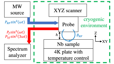
The setup of our near-field magnetic microwave microscope (identical to that described in Ref. Oripov et al. (2019)) is described in this section. A schematic of the setup is shown in Fig. 1.
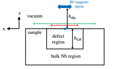
The heart of our microwave microscope is the magnetic writer head (provided by Seagate Technology) that is used in conventional hard-disk drives. The central part of the magnetic writer head is basically a solenoid that generates a localized RF magnetic field. The solenoid is in the sub-micron scale, which sets the spatial resolution of our microscope. In the setup, a Seagate magnetic writer head is attached to a cryogenic XYZ positioner (sub-micron spatial resolution) and used in a scanning probe microscope fashion. The probe is in contact with the sample during the third harmonic measurement. However, the surfaces of the probe and sample are not perfectly flat, resulting in a finite probe-sample separation , estimated to be less than 1 micron.
The microwave source signal is sent to the probe (magnetic writer head) by its built-in and highly-engineered transmission line. The probe then produces a local (sub-micron scale) RF magnetic field acting on the sample surface. The superconducting sample then generates a screening current on the surface in an effort to maintain the Meissner state. This screening current generates a response magnetic field that is coupled back to the same probe, creating a propagating signal whose third harmonic component is measured by a spectrum analyzer at room temperature. is measured because it arises from both the nonlinear Meissner effect Groll et al. (2010); Makita et al. (2022), and when a vortex penetrates the sample surface and forms a vortex semi-loop Gurevich and Ciovati (2008) (as discussed in Sec. I), either due to an intrinsic mechanism or local defects (weak spot for a vortex to penetrate).
measurements of superconductor nonlinear response show tremendous dynamic range, often more than 50 dB Tai et al. (2011, 2012, 2014b, 2015); Oripov et al. (2019). The excellent instrumental nonlinear background of our measurements ( -155 dBm) allows for very sensitive measurements of superconductor nonlinearity and its variation with temperature, driving RF power, location, and probe-sample separation. Note that measurements are recorded in dBm and later converted to linear power for further study.
To improve the signal-to-noise ratio, microwave filters are installed as follows. Low pass filters are installed between the microwave source and the probe to block the unwanted harmonic signals generated by the microwave source. High pass filters are installed between the probe and the spectrum analyzer to block the fundamental input frequency signal from reaching the spectrum analyzer and producing unwanted nonlinear signals.
Measurements are performed with a variety of fixed input frequencies between 1.1 GHz and 2.2 GHz, while varying temperature and applied RF field amplitude. No external DC magnetic field is applied. The measured residual DC field near the sample at low temperatures is around 35 T, as measured by a cryogenic 3-axis magnetometer.
The base temperature for a sample in the cryostat is around 3.5 K. The sample and the thermometer are both directly mounted on the cold plate to ensure good thermalization.
III Experimental results
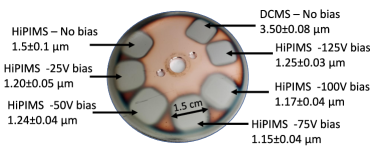
In this work, we study seven Nb films deposited on one common Cu substrate, as shown in Fig. 2. One of the samples is prepared by Direct Current Magnetron Sputtering (DCMS) with zero bias, and the sample thickness is around 3.5 m. The other six samples are prepared by High Power Impulse Magnetron Sputtering (HiPIMS), with bias from 0 V to 125 V, and the sample thickness ranges from 1.15 m to 1.5 m. The preparation of the seven Nb/Cu films is discussed in Appendix A. In the following, the HiPIMS 25 V bias Nb/Cu sample is discussed in detail, and the results of all the seven Nb/Cu samples are summarized and compared in Table 2 and in Table 3.
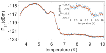
Fig. 3 shows the representative data for the third harmonic response power as a function of temperature at a fixed location on the HiPIMS 25 V bias Nb/Cu sample. A representative measurement protocol is as follows. The sample is warmed up to 10 K (above ), and then the microwave source is turned on with fixed input frequency (=1.86 GHz) and input power (=+2 dBm), and then is measured as the sample is gradually cooled down to 3.5 K. In other words, the surface of the sample experiences a fixed RF field in a sub-micron scale area during the cooldown process from 10 K to 3.5 K.
The measured in Fig. 3 can be decomposed into three segments: the region above 9.1 K, the region below 6.7 K, and the region in between. The magnetic writer head (the probe of our microwave microscope) itself has temperature-independent nonlinearity. above 9.1 K comes from this probe background and is indeed temperature-independent. A transition around 9.1 K can be seen in the inset of Fig. 3. This transition around 9.1 K comes from the intrinsic nonlinear response of the Nb film. The strongest signal here shows up below 6.7 K. In the following, such a onset temperature is called the transition temperature and is denoted as . Compared to the signal around 9.1 K, the onset around 6.7 K is dramatic. Such a signal suggests that some mechanism shows up at and below 6.7 K that produces strong nonlinearity. In summary, in Fig. 3 can be understood as the combination of three different sources of nonlinearity: temperature-independent probe background, that related to intrinsic Nb response, and mechanisms showing up at and below 6.7 K. The mechanisms leading to strong below 6.7 K are extrinsic and are likely due to surface defects. Note that below 6.7 K is much stronger than the intrinsic Nb signal around 9.1 K, suggesting that our local measurement is sensitive to surface defects.
Since the main objective of this work is investigating RF properties of surface defects, the strong below 6.7 K is the main focus in the following.
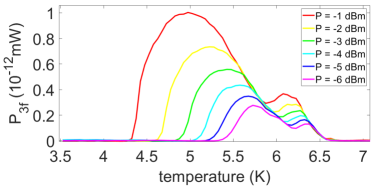
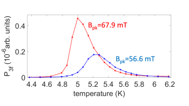
To further study the nature of below 6.7 K, for various input powers (and hence various applied RF field amplitudes ) are measured. For each measurement, the sample is warmed up to 10 K and then cooled down to 3.5 K while experiencing an applied RF field with fixed input frequency and input power. Since the measured is the combination of probe background and sample contribution, the probe background (probe background is obtained by averaging the magnitude of between 9.5 K and 10 K) is subtracted from the total signal to isolate the sample signal. The process is repeated six times, each time with a different input power. The results of the six of different input powers/RF field amplitudes are shown in the linear format in Fig. 4.
In Fig. 4, all the six exhibit a two-peak feature, and their are consistently around 6.7 K. The two-peak feature suggests that there might be two distinct mechanisms, or features, of nonlinearity. For both peaks, as the RF field amplitude increases (purple to red in Fig. 4), the maximum increases; in addition, the maximum and the low-temperature end both show up at a lower temperature. These features of are listed in Table 1. We will see that the four features of listed in Table 1 are the key features of all the nonlinear data in the sense that they show up in all the Nb/Cu films measurement results (see Fig. 4 and Fig. 6) and also in numerical simulations of superconductor nonlinear response (see Fig. 9, Fig. 13, and Fig. 14).
![[Uncaptioned image]](/html/2305.07746/assets/x5.png)
As discussed in Sec. I, is strong in the presence of magnetic vortices. In Sec. IV, we explore this idea further and show that the four key features of (Table 1) can be understood by vortex nucleation (either due to intrinsic mechanisms or extrinsic surface defects) and the vortex penetration field .
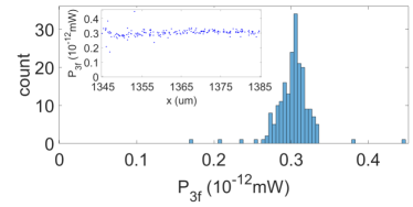
So far the measurements are taken at one single location on the surface of the sample. How about the situation at other locations? In particular, does the defect signal (the strong below 6.7 K) show up at other locations as well? To answer this question, a one-dimensional (1D) scan is performed for a 40 m range with a step size of 0.2 m. Temperature and input power are chosen to be T = 5.7 K and P = -5 dBm, and our goal is to determine the homogeneity of the signal from the lower temperature peak of the blue curve in Fig. 4. The 1D scan result is shown in Fig. 5. According to this scanning result, the signal from the defect is quite consistent and uniform at the m-scale (coefficient of variation = 0.08). One possible explanation of such uniformity is that the size of one single defect is at the nm-scale, and hence the signal of our sub-micron scale measurements comes from the contributions of multiple defects. A measurement technique with nm-scale spatial resolution is required to explore the RF properties of one single defect (scan across one single grain boundary, for example).
![[Uncaptioned image]](/html/2305.07746/assets/x8.png)
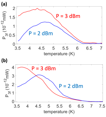
So far only the HiPIMS 25 V bias Nb/Cu sample has been discussed. and its temperature dependence and input power dependence are studied for the other six Nb/Cu samples in the same manner as the HiPIMS 25 V bias Nb/Cu sample. The HiPIMS 25 V bias Nb/Cu sample shows the two-peak feature, suggesting that the measured is the superposition of two defect signals. On the other hand, for some of the Nb/Cu samples (75 V bias, 100 V bias, 125 V bias), the defect signal shows a single-peak structure, suggesting that the measured captures only one defect signal. Fig. 6 shows the representative for the 75 V bias sample (Fig. 6 (a)) and the 125 V bias sample (Fig. 6 (b)). For both Fig. 6 (a) and (b), displays Features 1, 2, and 3 (Table 1), suggesting that these features are quite universal. Although we have no access to the temperature regime below 3.5 K, Feature 4 (Table 1) is likely to be present based on above 3.5 K.
Besides these common features, Fig. 6 (a) and Fig. 6 (b) do have a qualitative difference. In Fig. 6 (a), a stronger RF field amplitude leads to a stronger (the red curve is above the blue curve) for all temperatures. In Fig. 6 (b), on the contrary, for K, a stronger RF field amplitude leads to a weaker (the red curve is below the blue curve). In Sec. IV.4, we will show that such a difference could be related to how deep an RF vortex semi-loop penetrates into a sample through a surface defect.
The results of the defect signal and the Nb signal of all seven Nb/Cu samples are summarized in Table 2. For the six HiPIMS Nb/Cu samples, it is quite universal that measurements reveal the intrinsic Nb signal around 9 K and the extrinsic defect signal at low temperatures. Specifically, the defect signal with between 6.3 K and 6.8 K is observed for five out of the six HiPIMS Nb/Cu samples, suggesting that such a defect is a generic feature for these HiPIMS Nb/Cu samples. Moreover, the defect signals are always much stronger than the intrinsic Nb signal around 9 K, like the situation shown in Fig. 3. Scanning measurements are performed for three HiPIMS samples (25 V bias sample, 50 V bias sample and 125 V bias sample), and the results show that the defect signals are quite uniform at the m-scale for all three samples. Data for the HiPIMS 50 V bias sample and the 100 V bias sample are shown in Appendix B.
IV Discussion
IV.1 Introduction to numerical simulations
In our measurements, the applied field is a localized RF magnetic field instead of a uniform DC magnetic field. In addition, the configuration of the RF magnetic field produced by the probe is non-uniform but is similar to the field produced by a point dipole. In other words, the situation is different from the case of “a constant DC magnetic field parallel to the sample surface”. As a result, it is required to study the third harmonic response more carefully.
The Time-Dependent Ginzburg-Landau (TDGL) model is widely used for studying vortex behavior in superconductors Oripov and Anlage (2020); Wang et al. (2022b); Carlson et al. (2021); Pack et al. (2020); Kato (1999); Lara et al. (2015); Dobrovolskiy et al. (2020); Hernández and Domínguez (2008). In particular, vortices (see Sec. IV.2) and the proximity effect (see Sec. IV.3) are incorporated naturally in TDGL simulations and hence TDGL is a good tool for SRF material science. To better understand our data, numerical simulations of the TDGL equations are performed. The full TDGL equations must be solved in this case because the superconductor is subjected to a time-dependent and inhomogeneous RF magnetic field. We do not assume or impose any spatial symmetries in the model, and solve Maxwell’s equations for the dipole in free space above the superconductor, as well as inside the superconductor Oripov and Anlage (2020). The TDGL equations solved are the same as those discussed in Ref. Oripov and Anlage (2020).
In the simulations, the smooth and flat superconducting sample occupies the region, and the magnetic writer probe is approximated to be a pointlike magnetic dipole with a sinusoidal time-dependent magnetic moment (namely an RF magnetic dipole pointing in the x direction) whose frequency is 1.7 GHz (=1.7 GHz). The RF dipole locates at with =400 nm. That is, the RF magnetic dipole is above the superconducting sample and parallel to the surface of the sample. Since the magnetic field produced by the RF dipole is non-uniform, the peak RF magnetic field amplitude experienced by the superconductor is specified and is denoted as . Here is the location in the sample that experiences the strongest field, and hence is the RF field amplitude at . Because the RF field is localized, nontrivial dynamics of the sample (vortex nucleation, for example) would show up only in the region that is underneath the RF magnetic dipole (namely near ), while the region that is far away from the RF magnetic dipole would be in the vortex-free Meissner state.
In the simulations, TDGL is used to calculate the time evolution of the order parameter and the vector potential as the superconducting sample is stimulated by the time-dependent RF field produced by the horizontal point dipole above it. (There is no DC magnetic field in the simulations.) With the order parameter and the vector potential, the screening current and hence the magnetic field associated with that screening current (response of the sample) can be calculated. The response magnetic field is calculated at the location of the point dipole and it is assumed that this time-varying magnetic field induces a voltage wave that propagates up to the spectrum analyzer at room temperature. is proportional to the third Fourier component of the magnetic field (generated by the screening current) at the dipole location.
Most TDGL treatments assume a 2D sample and fields that are uniform in the third dimension. This oversimplifies the problem. It creates “artificial features that extend uniformly” in the third dimension and thus creates infinitely long vortices in the superconductor. Our approach (multi-domain 3D simulation) does not make such unrealistic assumptions. In addition, our experiment and model examine the properties of magnetic vortex semi-loops, which are thought to be the generic types of RF vortex excitations created at the surface of SRF cavities Gurevich and Ciovati (2008).
In the following, we first consider the case of a defect-free bulk Nb ( K) (Sec. IV.2) for developing central concepts relevant to nonlinear response and then propose a surface defect model (Sec. IV.3) whose shares common features with the experimental results (the four key features in Table 1). After that, we consider the surface defect model with various defect heights (Sec. IV.4) and show that can reveal how deep an RF vortex semi-loop penetrates into a sample through a surface defect. We then study another surface defect model (Sec. IV.5) and compare its with the of the first surface defect model and show that can reveal how many RF vortex semi-loops are nucleated by surface defects in each half of the RF cycle. With physical insights gained by these simulations, the Nb/Cu films can be compared further (Sec. IV.6), and the best Nb/Cu film for SRF applications can be identified.
Parameters for all the TDGL simulations are given in Appendix D.
IV.2 Calculated bulk Nb nonlinear response
Unlike a DC vortex whose behavior shows no time dependence, an RF vortex shows nontrivial dynamics, and should be examined in a time-domain manner. Here we demonstrate the time-domain analysis (focusing on the dynamics of RF vortices) for a specific RF field amplitude ( mT) and a specific temperature (8.23 K). (Material parameters of Nb are used in the defect-free bulk Nb simulations. See Appendix D.)
The dynamics of RF vortex semi-loops for bulk Nb during the first half of an RF cycle (frequency=1.7 GHz, period=s) is shown in Fig. 7, for a fixed RF field amplitude ( mT) and a fixed temperature (8.23 K). Fig. 7 (a)-(g) show the space and time dependence of the square of the normalized order parameter () (here 1 means full superconductivity and 0 means no superconductivity); the black region is where . Since the order parameter is suppressed significantly at the center of a vortex core, a vortex can be visualized by tracking the black region. Here is the value of the order parameter deep inside bulk Nb at temperature T.
In the early stage of the RF cycle, there is no RF vortex (Fig. 7 (a) and (b)), and then an RF vortex semi-loop that is parallel to the direction of the RF dipole (which points in the x direction) shows up (Fig. 7 (c), (d), (e) and (g)). The RF vortex semi-loop disappears later in the RF cycle (Fig. 7 (f)).
Besides examining the spatial distribution of the order parameter, another signature of vortices is the phase of the order parameter. Because Ginzburg-Landau theory is based on the existence of a single-valued complex superconducting order parameter (), the phase must change by integral multiples of in making a closed contour (see equation (4.45) in Tinkham (2004)), namely
where N is a positive or negative integer, or zero. The integral is quantized, and corresponds to the number of vortices enclosed by the closed contour.
Fig. 7 (i) shows the value of the integral (namely ) as a function of time. The contour is on the YZ plane and is large enough to enclose the entire nontrivial region. Note that Fig. 7 (h) and Fig. 7 (i) share a common horizontal axis. Based on Fig. 7 (i), there are no vortices at the moments of (a), (b) and (f), and there is one vortex at the moments of (c), (d) and (e), which agrees with the order parameter analysis (Fig. 7 (a)-(g)).
The time-domain analysis described here (space and time dependence of the order parameter (Fig. 7 (a)-(g)) and (Fig. 7 (i))) is applied to all TDGL simulations whenever we check whether or not there are RF vortex semi-loops.
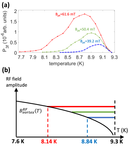
Equipped with the picture of RF vortex nucleation, now let’s move on to the resulting . The simulation result of for a fixed RF field amplitude ( mT) for bulk Nb is shown in Fig. 8 (a). The bell-shaped structure in Fig. 8 (a) can be decomposed into three segments (separated by the two dashed vertical black lines) and can be understood with the vortex penetration field (see Fig. 9) and the strength of superconductivity. An RF vortex semi-loop shows up when . Below 8.1 K, and hence the entire bulk Nb is in the vortex-free Meissner state (see Fig. 8 (b) and the purple curve in (f)), whose nonlinear response is weak. As temperature increases, decreases and hence would be greater than at a certain temperature depending on the strength of the RF stimulus. In this simulation ( mT), from the full time-domain simulation (see the discussion for Fig. 7) one finds that there is one RF vortex semi-loop (underneath the RF magnetic dipole) that penetrates the surface of the bulk Nb when the temperature is around 8.14 K (see Fig. 8 (c) and the blue curve in (f)). Roughly speaking, this implies that mT. drops/vortex nucleation is favorable as temperature increases, and indeed the second RF vortex semi-loop shows up around 8.6 K (see Fig. 8 (e) and the red curve in (f)) and thus increases with temperature between 8.1 K and 8.8 K. Besides examining the order parameter (Fig. 8 (b)-(e)), Fig. 8 (f) also shows how the vortex number changes with temperature.
The nonlinear response of the superconductor is determined not only by the number of vortices (as described above in the language of ) but also by the strength of superconductivity. As the temperature approaches the transition temperature of a superconductor, its superconductivity and hence nonlinear response becomes weak. Such a temperature dependence leads to the decreasing tail of above 8.8 K in Fig. 8 (a).
The simulation indicates that and the presence of RF vortex semi-loops are indeed closely related. Specifically, is weak as the bulk Nb is in the vortex-free Meissner state (below 8.1 K) and is strong in the presence of RF vortex semi-loops (above 8.1 K).
Fig. 9(a) summarizes the simulation results of for three different RF field amplitudes for bulk Nb. For all three RF field amplitudes, is weak at low temperatures (, vortex-free Meissner state), arises at high temperatures (, RF vortex semi-loops), and then drops with temperature as the temperature is near the critical temperature. For the red curve, the first vortex semi-loop shows up around 8.14 K, which implies ; for the blue curve, the first vortex semi-loop shows up around 8.84 K, which implies . Fig. 9(b) illustrates and the RF field amplitude dependence of the temperature range of ’s bell-shaped structure. In this RF field amplitude-temperature phase diagram, the vortex-free Meissner state occupies the region below and RF vortex semi-loops show up in the region above . It is clear that the ’s bell-shaped structure extends to lower temperatures as the RF field amplitude becomes stronger (from the blue to the green to the red in Fig. 9(a) and (b)) because of the temperature dependence of , and this explains Feature 4 in Table 1. Note that the four key features of (Table 1) are clearly observed in Fig. 9(a) (except that the onset temperature of is equal to but not below 9.3 K since this simulation is for a defect-free bulk Nb), suggesting that these key features are signatures of RF vortex nucleation.
Equipped with the intuition of and RF vortex semi-loops and their temperature dependence and RF field amplitude dependence for the defect-free bulk Nb, now let’s move on to the case with surface defects, which is the main focus of this paper.
IV.3 Simulation of vortex nucleation in grain boundaries
It is known that surface defects can serve as weak spots for RF vortex nucleation. The dynamics of RF vortices penetrating a sample surface through surface defects can be analyzed from two aspects: how many RF vortices are nucleated by surface defects, and how deep do RF vortices travel into a sample through surface defects in half an RF cycle? These two ideas could apply to RF vortex nucleation by various surface defects (grain boundaries, dislocations, etc.). In the following, we consider RF vortex nucleation in the case of grain boundaries, but the lessons of the features of and RF vortex nucleation should be generic.
As discussed in Sec. I, various kinds of surface defects could exist in SRF materials. One possible scenario of surface defects is that the grain boundaries of Nb are filled with the oxide of Nb Sung et al. (2013). The oxidation of Nb when it is exposed to air is a well-known phenomenon Yoon et al. (2008); Proslier et al. (2008); Romanenko and Schuster (2017); Semione et al. (2019, 2021); Halbritter (1987). In such oxidation, oxygen forms a solid solution in Nb and produces materials with critical temperatures below the bulk of pure Nb (9.3 K) DeSorbo (1963); Koch et al. (1974); Weingarten (2023). Nb samples with higher oxygen content tend to have a lower critical temperature. For instance, drops to around 7.33 K for 2% oxygen content, and drops to around 6.13 K for 3.5% oxygen content Koch et al. (1974).
Motivated by the oxidation of Nb in grain boundaries, here we model the oxide of Nb as a low- material (impurity phase) and consider a surface defect model that the grain boundaries of Nb are filled with the low- material. Such grain boundaries might serve as weak spots for vortex nucleation. As shown later in this section, the proximity effect is active in the grain boundaries. Here we consider one possible toy model realization of “Nb grain boundaries filled with low- material”. Of course, the toy model (a grain boundary model) considered here is just one possible scenario of surface defects that might be able to qualitatively explain the experimental results.
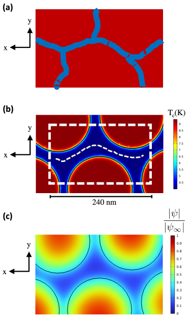
The RF dipole locates at and hence vortex semi-loops first show up near . Therefore, the physics around the origin plays a dominant role. As an approximation, surface defects (Nb grain boundaries filled with low- material) are introduced near the origin (illustrated in Fig. 10), while the region far away from the origin is set to be defect-free bulk Nb to reduce computational time. As a result, only the region around the origin characterizes the grain boundary scenario accurately, and thus the screening current is collected only from such an accurate region when calculating .
Fig. 10 shows the side view of the grain boundary model. As a surface defect model, the grain boundary extends (in the z direction) from the sample’s surface to a finite depth (grain boundary height), and the region below is set to be bulk Nb. (: sample surface; : defect whose XY cross-section is shown in Fig. 11 (b); : bulk Nb). Here the grain boundary height is set to be 200 nm.
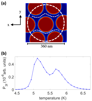
The side view of the grain boundary model is shown in Fig. 10, and the top view () is shown in Fig. 11. Fig. 11 (a) is an illustration of an Nb surface containing Nb grains (red) and grain boundaries filled with a low- impurity (blue). The realization used in the TDGL simulations is shown in Fig. 11 (b). Fig. 11 (b) is a top view of the sample’s critical temperature distribution around the origin of the grain boundary model: the red region means Nb with K, and the blue region means low- impurity with K. (Parameters of the grain boundary model are given in Appendix D.) The origin is at the center of Fig. 11 (b). The geometry is intentionally asymmetric in both the x direction and the y direction to prevent symmetry-induced artifacts. A top view of the sample’s critical temperature distribution with a broader scope (containing the defect region together with the bulk Nb region) is shown in Appendix E.
An RF vortex semi-loop that nucleates in the sample tends to be parallel to the direction of the RF dipole, which points in the x direction. Therefore, as , RF vortex semi-loops show up in the grain boundaries that are roughly parallel to the x direction. There is one grain boundary in Fig. 11 (b) that is roughly parallel to the x direction and it is marked by a white dashed curve. Grain boundaries are well-characterized inside the white dashed rectangle (the accurate region), and hence the screening current contribution to the signal recovered at the location of the dipole is collected only from inside the white dashed rectangle when calculating .
It is worth mentioning that the proximity effect shows up naturally in TDGL simulations. Fig. 11 (c) shows a snapshot of the distribution of normalized order parameter (here 1 means full superconductivity and 0 means no superconductivity) obtained by a TDGL simulation with the temperature being 5.4 K and mT. This snapshot is taken at the end of an RF cycle, namely when the RF field drops to zero ( and hence ). Due to the proximity effect, the normalized order parameter of the dark blue region is around 0.15 but not zero, even though the temperature (5.4 K) is higher than (4 K). As a result, a grain boundary filled with a low- impurity can host RF vortices even for .
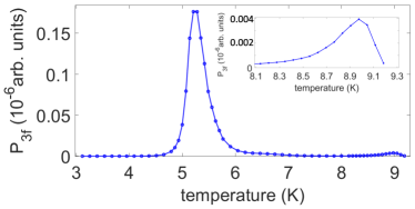
Fig. 12 shows the simulation result of for the grain boundary model shown in Fig. 10 (side view of the model) and Fig. 11 (top view of the model). Compared to the around 9 K, the between 4.5 K and 6 K is much stronger. In other words, in the presence of surface defects, generated by surface defects is much stronger than the intrinsic of Nb. In the following, we focus on the generated by surface defects.
Fig. 13 shows the simulation result of for two different RF field amplitudes for the grain boundary model. At low temperatures, the sample is in the Meissner state and is weak. As temperature increases, RF vortex semi-loops nucleate in the grain boundary marked by the white dashed curve in Fig. 11 (b) and result in strong . (The existence of RF vortex semi-loops is verified by examining the order parameter in a time-domain manner as described in Fig. 7.) This can be interpreted as , where is the vortex penetration field of the region around that specific grain boundary. Note that RF vortex semi-loops show up in the grain boundary, indicating that the grain boundary serves as the weak spot for RF vortex nucleation.
Here the upper onset temperature of is around 5.9 K. The grain boundary model is a mixture of the K Nb and the K impurity, and hence is between 4 K and 9.3 K. Of course, the numerical value of depends on how the Nb and the impurity are distributed. Our objective with this model is not to propose a specific microstructure of the sample, but to illustrate the generic nonlinear properties of a proximity-coupled defective region of the sample.
Similar to the case of bulk Nb (Fig. 9(a)), in Fig. 13 also exhibits the four key features (Table 1). Therefore, the ideas illustrated in Fig. 9(b) could describe the physics of the grain boundary model, with being 5.9 K but not 9.3 K and being the vortex penetration field of the region around the specific grain boundary, but not a bulk property. The fact that experimental data (Fig. 4 and Fig. 6) and TDGL simulation of the grain boundary model (Fig. 13) both exhibit the four key features (Table 1) and a below 9.3 K suggests that “RF vortex semi-loops nucleate in grain boundaries full of low- impurity” is indeed one of the possible mechanisms of the observed signals for the HiPIMS Nb/Cu samples.
IV.4 Effect of height of grain boundaries on
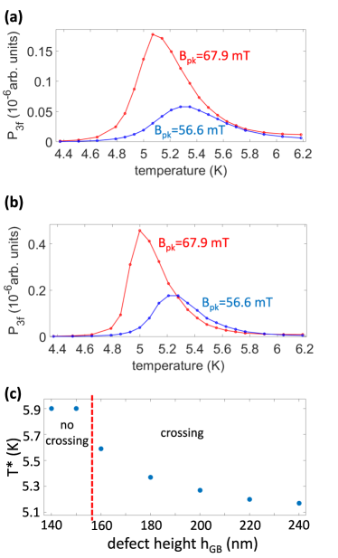
If the RF field amplitude is not very strong, RF vortex semi-loops would stay in grain boundaries () instead of entering the bulk Nb regions. Therefore, determines how deep an RF vortex semi-loop penetrates into a sample through a surface defect. In Sec. IV.3, the grain boundary height is set to be 200 nm. Here we consider the effect of varying , with everything else being the same as described in Sec. IV.3.
Fig. 14 (a) and (b) show the results for nm and nm, respectively. Fig. 14 (a) is similar to Fig. 6 (a), in the sense that a stronger RF field amplitude leads to a stronger (the red curve is above the blue curve) for all temperatures; Fig. 14 (b) is similar to Fig. 6 (b), in the sense that shows a “crossing” effect: a stronger RF field amplitude leads to a weaker (the red curve is below the blue curve) for temperatures close to . The temperature where the red curve ( with a strong RF field amplitude) and the blue curve ( with a weak RF field amplitude) cross is denoted as . For Fig. 14 (a), there is no crossing and hence K. For Fig. 14 (b), . Fig. 14 (c) shows how crossing temperature changes with grain boundary height . For a shallow grain boundary (small ), there is no crossing and hence . The crossing shows up when the grain boundary is beyond a critical depth. As grain boundary height becomes larger, the crossing effect becomes more significant ( becomes smaller, which means that the temperature window that a stronger RF field amplitude leads to a weaker becomes larger) and eventually tends to saturate.
The crossing effect can be understood as follows. In experiments/simulations, is collected by the magnetic writer/at the RF dipole location, which is at (above the sample surface). For a weak RF field amplitude, the RF vortex semi-loop in the grain boundary stays close to the sample’s surface (). As the RF field amplitude increases, the RF vortex semi-loop in the grain boundary is pushed toward the bottom of the grain boundary ()(see Appendix F), which means that the RF vortex semi-loop is farther away from the magnetic writer/the RF dipole location (), and hence the measured becomes weaker. Such a phenomenon shows up only when the RF vortex semi-loop in the grain boundary can be pushed far away from the sample surface. For a shallow grain boundary, the RF vortex semi-loop always stays just below the sample surface instead of penetrating deep into the sample, and hence doesn’t decrease as the RF field amplitude increases (no crossing effect).
The crossing effect is quantified by , which could be related to how deep an RF vortex semi-loop penetrates into a sample through a surface defect (denoted as ).
IV.5 Simulation of a defect model with two grain boundaries
In the grain boundary model discussed in Sec. IV.3 and Sec. IV.4, there is only one single grain boundary underneath and roughly parallel to the RF dipole, and thus RF vortex semi-loops nucleate in one single grain boundary and shows a single-peak feature. Such a scenario corresponds to the case that the sample’s grain boundary density is low. For a sample whose grain boundary density is high, it can be modeled as a grain boundary model that contains two grain boundaries underneath and roughly parallel to the RF dipole.
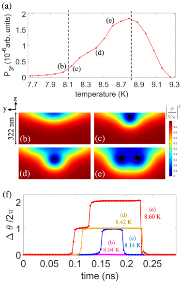
Here we consider a grain boundary model that contains two grain boundaries that are near the origin and roughly parallel to the x direction. The basic setting of the model is the same as described in Sec. IV.3. The only difference is how the Nb and the impurity are distributed horizontally, as shown in Fig. 15 (a). Fig. 15 (a) shows the top view of the critical temperature distribution and Fig. 15 (b) shows the TDGL simulation result of for this model.
in Fig. 15 (b) exhibits a two-peak feature, which can be understood as follows. At low temperatures, the sample is in the Meissner state and is weak. As temperature increases, around 4.93 K an RF vortex semi-loop nucleates in the top grain boundary and results in the lower temperature peak, and then around 5.67 K another RF vortex semi-loop nucleates in the bottom grain boundary and results in the higher temperature peak. The nucleation of the two RF vortex semi-loops is verified by monitoring (the same analysis as shown in Fig. 8). Note that the two-peak feature of the in Fig. 15 (b) (simulation) is also observed in Fig. 4 (measurement).
In this model, RF vortex semi-loops nucleate in both grain boundaries and thus result in the two-peak feature of . On the contrary, in Sec. IV.3 and Sec. IV.4, there is only one RF vortex semi-loop nucleate in one grain boundary and thus results in the single-peak feature of . In other words, the number of peaks is an indication of the density of surface defects that nucleate RF vortex semi-loops.
IV.6 Nb/Cu samples comparison
![[Uncaptioned image]](/html/2305.07746/assets/x18.png)
Larger values of are closely related to the presence of RF vortex semi-loops. By studying , we investigate surface defects that nucleate RF vortex semi-loops, which are the kinds of surface defects that are closely related to the RF performance of SRF cavities. Surface defects that don’t nucleate RF vortex semi-loops are beyond consideration here. For example, if a grain boundary is too narrow (much smaller than the coherence length of a sample) to nucleate an RF vortex semi-loop, it would be less likely to produce large amounts of . Such a grain boundary is likely to be harmless to SRF applications. In the following, surface defects refer to the kind of surface defects that nucleate RF vortex semi-loops.
Equipped with the simulation results, of surface defects can be analyzed further. First, the number of peaks can be related to the density of surface defects (). Single-peak corresponds to a low density of surface defects, and two-peak corresponds to a high density of surface defects. Second, the crossing effect of can be related to how deep an RF vortex semi-loop penetrates into a sample through a surface defect (). (no crossing) corresponds to a small (shallow), and (crossing) corresponds to a large (deep).
The assignment of qualitative surface defect properties of all seven Nb/Cu samples are summarized in Table 3. The first column shows an estimate for the density of surface defects () and the second column shows how deep an RF vortex semi-loop penetrates into a sample through a surface defect (). RF vortex penetration through surface defects is one of the main enemies of SRF applications. To achieve good SRF performance, the surface defect density should be low and the defect should be shallow. From the point of view of these two properties, the HiPIMS 75 V bias Nb/Cu sample is the best sample among the five HiPIMS Nb/Cu samples that have non-zero voltage bias.
In the numerical simulations of this work, surface defects that nucleate RF vortex semi-loops are modeled as grain boundaries. Since is associated with the behavior of RF vortex semi-loops, it is likely that the ideas of (how many RF vortex semi-loops nucleated by surface defects) and (how deep RF vortex semi-loops travel) could apply to surface defects other than grain boundaries (dislocation tangles, for example).
V Conclusion
In this work, we study seven Nb/Cu films that are candidates for SRF applications. Local measurements reveal surface defects with onset temperatures between 6.3 K and 6.8 K for five out of the six HiPIMS Nb/Cu samples, indicating that such defects are a generic feature of these air-exposed HiPIMS Nb/Cu films. coming from the low- surface defect is much stronger than the intrinsic Nb response around 9 K, suggesting that our local measurement is sensitive to surface defects. With the capability of m-scale scanning, it is found that such a defect is quite uniform in space on the m-scale.
TDGL simulations are performed to analyze the experimental results further. In particular, the simulations suggest that the density of surface defects that nucleate RF vortices and how deep RF vortices travel through these surface defects can be extracted qualitatively from our local measurements. From the point of view of these two properties, the HiPIMS 75 V bias Nb/Cu sample is the best sample for SRF applications.
VI Acknowledgement
The authors would like to thank Javier Guzman from Seagate Technology for providing magnetic write heads. C.Y.W. would like to thank Bakhrom Oripov and Jingnan Cai for helpful discussions. This work is funded by the U.S. Department of Energy/High Energy Physics through grant No. DESC0017931 and the Maryland Quantum Materials Center.
Appendix A Sample preparation
![[Uncaptioned image]](/html/2305.07746/assets/x19.png)
Here we discuss how the seven Nb/Cu films studied in this paper are prepared.
The substrate used for the Nb coatings is a 2 mm thick, oxygen-free electronic (OFE) copper disk measuring 75 mm in diameter. Prior to coating, the substrate disk is degreased using commercial detergent. The sample is then chemically polished using a mixture of sulfamic acid (, 5 g/L), hydrogen peroxide (, 5% vol.), n-butanol (5% vol.) and ammonium citrate (1 g/L) heated up at 72 for 20 minutes. After polishing, the disk is rinsed with sulfamic acid to remove the build-up of native oxide and cleaned with de-ionized water and ultra-pure ethanol.
The Cu substrate is mounted on an ultra-high vacuum (UHV) stainless steel chamber equipped with a rotatable shutter to expose in turn the areas to be coated, and the chamber is then connected to a sputtering system. Both assemblies are performed inside an ISO5 cleanroom, and the sputtering apparatus is described in detail in Rosaz et al. (2022). The entire system is transported to the coating bench where it is coupled to the pumping group and gas injection lines, and pumped down to about mbar. The pumping group and the sputtering system undergo a 48-hour bakeout at 200, during which a 4-hour activation of the Non-Evaporable Getter (NEG) pump is performed. The temperature of the UHV chamber is maintained at 150 until the start of the coating. After cooling down, the system reaches a base pressure around mbar. Ultra-pure krypton (99.998%) is injected into the system until a process pressure of mbar is reached. The seven coatings are then performed according to the deposition parameters outlined in Table 4. One of the samples is prepared by Direct Current Magnetron Sputtering (DCMS) with zero bias, and the coating thickness is around 3.5 m. The other six samples are prepared by High Power Impulse Magnetron Sputtering (HiPIMS), with bias voltages ranging from 0 V to -125 V, with coating thicknesses ranging from 1.15 m to 1.5 m.
During the coating process, the cavity temperature was monitored with an infrared thermal sensor (OMEGA OS100-SOFT) and kept constant at 150. The HiPIMS plasma discharge was maintained using a pulsed power supply (Huettinger TruPlasma HighPulse 4006) and the negative bias voltage was applied to the samples using a DC power supply (TruPlasma Bias 3018). The DCMS discharge was maintained using a Huettinger Truplasma 3005 power supply. The discharge and bias voltages and currents were monitored throughout the entire coating process using voltage (Tektronix P6015A) and current (Pearson current monitor 301×) probes whose signals are recorded by a digital oscilloscope (Picoscope 2000). After the coating, the samples were cooled down to room temperature, after which the chamber was vented with dry air. The Nb layer thickness is measured by X-ray fluorescence via the attenuation method.
Appendix B Data for the HiPIMS 50 V bias and 100 V bias Nb/Cu sample
Here we show the representative data for generated by surface defects for the HiPIMS 50 V bias and 100 V bias Nb/Cu sample. For the HiPIMS 50 V bias sample, with around 6.4 K is observed in a strong input power regime (Fig. 16 (a)), and with around 6.8 K is observed in a weak input power regime (Fig. 16 (b)). For the HiPIMS 100 V bias sample, with around 6.5 K is observed (Fig. 16 (c)).
Appendix C Check for hysteresis in measurements
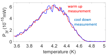
Here we check whether or not measurements exhibit hysteresis. The HiPIMS 125 V bias Nb/Cu sample first undergoes a cool down from 10 K to 3.6 K with zero RF field. The microwave signal is turned on after the temperature stabilizes at 3.6 K. The sample then gradually warms up from 3.6 K to 10 K (warm up ), and then cools down from 10 K to 3.6 K (cool down ), with the microwave signal being turned on in this process. As shown in Fig. 17, such measurement does not exhibit a clear hysteresis.
Appendix D Parameters for TDGL simulations
![[Uncaptioned image]](/html/2305.07746/assets/x22.png)
Values of parameters used in TDGL simulations are summarized in Table 5. The “impurity” sector specifies the material parameters of the low- impurity in the two surface defect models (Sec. IV.3, Sec. IV.4 and Sec. IV.5).
Material parameters (penetration depth , Ginzburg-Landau parameter , etc.) of Nb films vary from one sample to sample. For the Nb part in the TDGL simulations, we adopt the material parameters of bulk Nb instead of Nb films for simplicity.
The choice of the material parameters of the low- impurity in the two surface defect models is based on the following considerations. For simplicity, the Ginzburg-Landau parameter of the low- impurity is taken to be the same as that of bulk Nb (). In experiments, typically the measured is strong at low temperatures (surface defects) and is weak around 9 K. To simulate such a feature, a mechanism that suppresses at high temperatures is required.
One possible mechanism is that superconductivity near the sample surface, including both the impurity region and the Nb region, is suppressed significantly when the low- impurity is above its transition temperature (), namely when K. As the temperature increases significantly above (around 9 K, for example), superconductivity is weak (and thus all of the responses related to the strength of superconductivity are weak, including ) even in the Nb region, due to the proximity effect. The question is, what kind of material parameters should be assigned to the low- impurity to achieve this feature at high temperatures?
The Ginzburg-Landau free energy is given by . One can naively extend Ginzburg-Landau theory to the regime above the transition temperature of a superconductor, where becomes positive (, with ). In that case, a large and positive (of the impurity) means that superconductivity is strongly suppressed, which means that the superconductivity in nearby superconductors (the Nb region in our case) is weak due to the proximity effect. A large and positive above implies a large below , which, in turn, implies a small penetration depth (). As a result, we choose a small (16.3 nm).
Appendix E A top view for the grain boundary model in Sec. IV.3
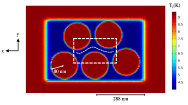
Fig. 11 (b) shows the region around the origin (which plays the dominant role in RF vortex nucleation and ) for the grain boundary model discussed in Sec. IV.3. Compared to Fig. 11 (b), Fig. 18 shows the setup over a broader range as indicated by the green dashed line in Fig. 10. Fig. 18 contains the entire defect region (the five Nb grains and the blue region) and part of the bulk Nb region as shown in Fig. 10.
Appendix F Snapshots of a vortex in a grain boundary for the grain boundary model in Sec. IV.3
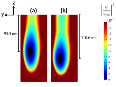
An RF vortex semi-loop is roughly parallel to the direction of the RF dipole, which points in the x direction, and hence the cross-section of the RF vortex semi-loop is on the YZ plane. Fig. 19 visualizes an RF vortex semi-loop in the grain boundary marked by the white dashed curve in Fig. 11 (b), with the vortex core corresponding to the black region, where . The RF vortex semi-loop penetrates the sample surface and the vortex core is around 93.5 nm deep for mT (Fig. 19 (a)) and is around 110.6 nm deep for mT (Fig. 19 (b)).
References
- Padamsee (2017) Hasan Padamsee, “50 years of success for srf accelerators—a review,” Superconductor science and technology 30, 053003 (2017).
- Bambade et al. (2019) Philip Bambade, Tim Barklow, Ties Behnke, Mikael Berggren, James Brau, Philip Burrows, Dmitri Denisov, Angeles Faus-Golfe, Brian Foster, Keisuke Fujii, et al., “The international linear collider: a global project,” arXiv preprint arXiv:1903.01629 (2019).
- Ciovati (2006) Gianluigi Ciovati, “Review of the frontier workshop and q-slope results,” Physica C: Superconductivity 441, 44–50 (2006).
- Gurevich (2006a) A. Gurevich, “Multiscale mechanisms of srf breakdown,” Physica C: Superconductivity 441, 38–43 (2006a).
- Gurevich (2012) Alex Gurevich, “Superconducting radio-frequency fundamentals for particle accelerators,” Reviews of Accelerator Science and Technology 5, 119–146 (2012).
- Gurevich (2017) Alex Gurevich, “Theory of rf superconductivity for resonant cavities,” Superconductor Science and Technology 30, 034004 (2017).
- Champion et al. (2009) Mark S. Champion, Lance D. Cooley, Camille M. Ginsburg, Dmitri A. Sergatskov, Rongli L. Geng, Hitoshi Hayano, Yoshihisa Iwashita, and Yujiro Tajima, “Quench-limited srf cavities: Failure at the heat-affected zone,” IEEE transactions on applied superconductivity 19, 1384–1386 (2009).
- Bao and Guo (2019) Shiran Bao and Wei Guo, “Quench-spot detection for superconducting accelerator cavities via flow visualization in superfluid helium-4,” Physical Review Applied 11, 044003 (2019).
- Posen et al. (2015a) S. Posen, N. Valles, and M. Liepe, “Radio frequency magnetic field limits of nb and nb 3 sn,” Physical review letters 115, 047001 (2015a).
- Kneisel et al. (2015) P. Kneisel, G. Ciovati, P. Dhakal, K. Saito, W. Singer, Xenia Singer, and G.R. Myneni, “Review of ingot niobium as a material for superconducting radiofrequency accelerating cavities,” Nuclear Instruments and Methods in Physics Research Section A: Accelerators, Spectrometers, Detectors and Associated Equipment 774, 133–150 (2015).
- Antoine (2019) C.Z. Antoine, “Influence of crystalline structure on rf dissipation in superconducting niobium,” Physical Review Accelerators and Beams 22, 034801 (2019).
- Weingarten (2023) Wolfgang Weingarten, “Field-dependent surface resistance for superconducting niobium accelerating cavities-condensed overview of weak superconducting defect model,” IEEE Transactions on Applied Superconductivity (2023).
- Yoon et al. (2008) Kevin E. Yoon, David N. Seidman, Claire Antoine, and Pierre Bauer, “Atomic-scale chemical analyses of niobium oxide/niobium interfaces via atom-probe tomography,” Applied Physics Letters 93, 132502 (2008).
- Proslier et al. (2008) Th Proslier, John F. Zasadzinski, L. Cooley, C. Antoine, J. Moore, J. Norem, M. Pellin, and K.E. Gray, “Tunneling study of cavity grade nb: Possible magnetic scattering at the surface,” Applied Physics Letters 92, 212505 (2008).
- Romanenko and Schuster (2017) A. Romanenko and D.I. Schuster, “Understanding quality factor degradation in superconducting niobium cavities at low microwave field amplitudes,” Physical Review Letters 119, 264801 (2017).
- Semione et al. (2019) Guilherme Dalla Lana Semione, A. Dangwal Pandey, S. Tober, J. Pfrommer, A. Poulain, J. Drnec, G. Schütz, T.F. Keller, H. Noei, V. Vonk, et al., “Niobium near-surface composition during nitrogen infusion relevant for superconducting radio-frequency cavities,” Physical Review Accelerators and Beams 22, 103102 (2019).
- Semione et al. (2021) Guilherme Dalla Lana Semione, Vedran Vonk, Arti Dangwal Pandey, Elin Grånäs, Björn Arndt, Marc Wenskat, Wolfgang Hillert, Heshmat Noei, and Andreas Stierle, “Temperature-dependent near-surface interstitial segregation in niobium,” Journal of Physics: Condensed Matter 33, 265001 (2021).
- Russo (2007) Roberto Russo, “Quality measurement of niobium thin films for nb/cu superconducting rf cavities,” Measurement Science and Technology 18, 2299 (2007).
- Kharitonov et al. (2012) Maxim Kharitonov, Thomas Proslier, Andreas Glatz, and Michael J. Pellin, “Surface impedance of superconductors with magnetic impurities,” Physical Review B 86, 024514 (2012).
- Carlson et al. (2021) Jared Carlson, Alden Pack, Mark K. Transtrum, Jaeyel Lee, David N. Seidman, Danilo B. Liarte, Nathan S. Sitaraman, Alen Senanian, Michelle M. Kelley, James P. Sethna, et al., “Analysis of magnetic vortex dissipation in sn-segregated boundaries in nb 3 sn superconducting rf cavities,” Physical Review B 103, 024516 (2021).
- Lee et al. (2007) P.J. Lee, A.A. Polyanskii, Zu-Hawn Sung, D.C. Larbalestier, C. Antoine, P.C. Bauer, C. Boffo, and H.T. Edwards, “Flux penetration into grain boundaries large grain niobium sheet for srf cavities: Angular sensitivity,” in AIP Conference Proceedings, Vol. 927 (American Institute of Physics, 2007) pp. 113–120.
- Polyanskii et al. (2011) A.A. Polyanskii, P.J. Lee, A. Gurevich, Zu-Hawn Sung, and D.C. Larbalestier, “Magneto-optical study high-purity niobium for superconducting rf application,” in AIP Conference Proceedings, Vol. 1352 (American Institute of Physics, 2011) pp. 186–202.
- Köszegi et al. (2017) J Köszegi, O. Kugeler, D. Abou-Ras, J. Knobloch, and R. Schäfer, “A magneto-optical study on magnetic flux expulsion and pinning in high-purity niobium,” Journal of Applied Physics 122, 173901 (2017).
- Wang et al. (2018) Mingmin Wang, Shreyas Balachandran, Thomas Bieler, Santosh Chetri, Chris Compton, Peter Lee, Anatolii Polyanskii, et al., “Investigation of the effect of strategically selected grain boundaries on superconducting properties of srf cavity niobium,” in 18th international conference on rf superconductivity (2018) p. 210.
- Wang et al. (2022a) Mingmin Wang, Anatolii Polyanskii, Shreyas Balachandran, Santosh Chetri, Martin A. Crimp, Peter J. Lee, and Thomas R. Bieler, “Investigation of the effect of structural defects from hydride precipitation on superconducting properties of high purity srf cavity nb using magneto-optical and electron imaging methods,” Superconductor Science and Technology 35, 045001 (2022a).
- Lee et al. (2020) Jaeyel Lee, Zugang Mao, Kai He, Tiziana Spina, Sung-Il Baik, Daniel L. Hall, Matthias Liepe, David N. Seidman, Sam Posen, et al., “Grain-boundary structure and segregation in nb3sn coatings on nb for high-performance superconducting radiofrequency cavity applications,” Acta Materialia 188, 155–165 (2020).
- Romanenko and Padamsee (2010) A. Romanenko and H. Padamsee, “The role of near-surface dislocations in the high magnetic field performance of superconducting niobium cavities,” Superconductor Science and Technology 23, 045008 (2010).
- Bieler et al. (2010) T.R. Bieler, N.T. Wright, F. Pourboghrat, C. Compton, K.T. Hartwig, D. Baars, A. Zamiri, S. Chandrasekaran, P. Darbandi, H. Jiang, et al., “Physical and mechanical metallurgy of high purity nb for accelerator cavities,” Physical Review Special Topics-Accelerators and Beams 13, 031002 (2010).
- Wang et al. (2022b) Qing-Yu Wang, Cun Xue, Chao Dong, and You-He Zhou, “Effects of defects and surface roughness on the vortex penetration and vortex dynamics in superconductor–insulator–superconductor multilayer structures exposed to rf magnetic fields: numerical simulations within tdgl theory,” Superconductor Science and Technology 35, 045004 (2022b).
- Ries et al. (2020) R. Ries, E. Seiler, F Gömöry, A. Medvids, C. Pira, and O.B. Malyshev, “Superconducting properties and surface roughness of thin nb samples fabricated for srf applications,” in Journal of Physics: Conference Series, Vol. 1559 (IOP Publishing, 2020) p. 012040.
- Dhakal et al. (2014) Pashupati Dhakal, Gianluigi Ciovati, Peter Kneisel, and Ganapati Rao Myneni, “Enhancement in quality factor of srf niobium cavities by material diffusion,” IEEE Transactions on Applied Superconductivity 25, 1–4 (2014).
- Gonnella et al. (2014) Dan Gonnella, Matthias Liepe, et al., “Cool down and flux trapping studies on srf cavities,” Proceedings of LINAC 2014 (2014).
- Kleindienst et al. (2015) Raphael Kleindienst, Andrew Burrill, Oliver Kugeler, and Jens Knobloch, Commissioning results of the HZB quadrupole resonator, Tech. Rep. (2015).
- Keckert et al. (2021a) S. Keckert, R. Kleindienst, O. Kugeler, D. Tikhonov, and J. Knobloch, “Characterizing materials for superconducting radiofrequency applications—a comprehensive overview of the quadrupole resonator design and measurement capabilities,” Review of Scientific Instruments 92, 064710 (2021a).
- Arzeo et al. (2022) Marco Arzeo, F. Avino, S. Pfeiffer, G. Rosaz, M. Taborelli, L. Vega-Cid, and W. Venturini-Delsolaro, “Enhanced radio-frequency performance of niobium films on copper substrates deposited by high power impulse magnetron sputtering,” Superconductor Science and Technology 35, 054008 (2022).
- Keckert et al. (2021b) S. Keckert, W. Ackermann, H. De Gersem, X. Jiang, AÖ Sezgin, M. Vogel, M. Wenskat, R. Kleindienst, J. Knobloch, O. Kugeler, et al., “Mitigation of parasitic losses in the quadrupole resonator enabling direct measurements of low residual resistances of srf samples,” Aip Advances 11, 125326 (2021b).
- James et al. (2012) Colt James, Mahadevan Krishnan, Brian Bures, Tsuyoshi Tajima, Leonardo Civale, Randy Edwards, Josh Spradlin, and Hitoshi Inoue, “Superconducting nb thin films on cu for applications in srf accelerators,” IEEE transactions on applied superconductivity 23, 3500205–3500205 (2012).
- Antoine et al. (2019) Claire Z. Antoine, M. Aburas, A. Four, F. Weiss, Y. Iwashita, H. Hayano, S. Kato, Takayuki Kubo, and T. Saeki, “Optimization of tailored multilayer superconductors for rf application and protection against premature vortex penetration,” Superconductor Science and Technology 32, 085005 (2019).
- Lamura et al. (2009) G. Lamura, M. Aurino, A. Andreone, and J-C Villégier, “First critical field measurements of superconducting films by third harmonic analysis,” Journal of Applied Physics 106, 053903 (2009).
- Antoine et al. (2010) C.Z. Antoine, S. Berry, S. Bouat, J.F. Jacquot, J.C. Villegier, G. Lamura, and A. Gurevich, “Characterization of superconducting nanometric multilayer samples for superconducting rf applications: First evidence of magnetic screening effect,” Physical Review Special Topics-Accelerators and Beams 13, 121001 (2010).
- Antoine et al. (2011) C.Z. Antoine, S. Berry, M. Aurino, J-F Jacquot, J-C Villegier, G. Lamura, and A. Andreone, “Characterization of field penetration in superconducting multilayers samples,” IEEE Transactions on Applied Superconductivity 21, 2601–2604 (2011).
- Antoine et al. (2013) C.Z. Antoine, J-C Villegier, and G. Martinet, “Study of nanometric superconducting multilayers for rf field screening applications,” Applied Physics Letters 102, 102603 (2013).
- Katyan and Antoine (2015) N. Katyan and C.Z. Antoine, Characterization of thin films using local magneometer, Tech. Rep. (2015).
- Aburas et al. (2017) Muhammad Aburas, C.Z. Antoine, Aurelien Four, et al., “Local magnetometer: first critical field measurement of multilayer superconductors,” in Proc. 18th Int. Conf. RF Superconductivity (SRF’17) (2017) pp. 830–834.
- Ito et al. (2019) Hayato Ito, H. Hayano, T. Kubo, T. Saeki, Y. Iwashita, R. Katayama, H. Tongu, Kyoto ICR, R. Ito, T. Nagata, et al., “Lower critical field measurement of thin film superconductor,” in 29textsuperscript th Linear Accelerator Conf.(LINAC’18), Beijing, China, 16-21 September 2018 (JACOW Publishing, Geneva, Switzerland, 2019) pp. 484–487.
- Ito et al. (2020) Hayato Ito, Hitoshi Hayano, Takayuki Kubo, and Takayuki Saeki, “Vortex penetration field measurement system based on third-harmonic method for superconducting rf materials,” Nuclear Instruments and Methods in Physics Research Section A: Accelerators, Spectrometers, Detectors and Associated Equipment 955, 163284 (2020).
- Lee et al. (2000) Sheng-Chiang Lee, C.P. Vlahacos, B.J. Feenstra, Andrew Schwartz, D.E. Steinhauer, F.C. Wellstood, and Steven M. Anlage, “Magnetic permeability imaging of metals with a scanning near-field microwave microscope,” Applied Physics Letters 77, 4404–4406 (2000).
- Lee and Anlage (2003) Sheng-Chiang Lee and Steven M. Anlage, “Spatially-resolved nonlinearity measurements of yba 2 cu 3 o 7- bicrystal grain boundaries,” Applied physics letters 82, 1893–1895 (2003).
- Lee et al. (2005a) Sheng-Chiang Lee, Mathew Sullivan, Gregory R. Ruchti, Steven M. Anlage, Benjamin S. Palmer, B. Maiorov, and E. Osquiguil, “Doping-dependent nonlinear meissner effect and spontaneous currents in high-t c superconductors,” Physical Review B 71, 014507 (2005a).
- Lee et al. (2005b) Sheng-Chiang Lee, Su-Young Lee, and Steven M. Anlage, “Microwave nonlinearities of an isolated long y ba 2 cu 3 o 7- bicrystal grain boundary,” Physical Review B 72, 024527 (2005b).
- Mircea et al. (2009) Dragos I. Mircea, Hua Xu, and Steven M. Anlage, “Phase-sensitive harmonic measurements of microwave nonlinearities in cuprate thin films,” Physical Review B 80, 144505 (2009).
- Tai et al. (2011) Tamin Tai, X. X. Xi, C.G. Zhuang, Dragos I. Mircea, and Steven M. Anlage, “Nonlinear near-field microwave microscope for rf defect localization in superconductors,” IEEE transactions on applied superconductivity 21, 2615–2618 (2011).
- Tai et al. (2012) Tamin Tai, Behnood G. Ghamsari, and Steven M. Anlage, “Nanoscale electrodynamic response of nb superconductors,” IEEE Transactions on Applied Superconductivity 23, 7100104–7100104 (2012).
- Tai et al. (2014a) Tamin Tai, B.G. Ghamsari, and Steven M. Anlage, “Modeling the nanoscale linear response of superconducting thin films measured by a scanning probe microwave microscope,” Journal of Applied Physics 115, 203908 (2014a).
- Tai et al. (2014b) Tamin Tai, Behnood G. Ghamsari, Thomas R. Bieler, Teng Tan, X. X. Xi, and Steven M. Anlage, “Near-field microwave magnetic nanoscopy of superconducting radio frequency cavity materials,” Applied Physics Letters 104, 232603 (2014b).
- Tai et al. (2015) Tamin Tai, Behnood G. Ghamsari, Tom Bieler, and Steven M. Anlage, “Nanoscale nonlinear radio frequency properties of bulk nb: Origins of extrinsic nonlinear effects,” Physical Review B 92, 134513 (2015).
- Oripov et al. (2019) Bakhrom Oripov, Thomas Bieler, Gianluigi Ciovati, Sergio Calatroni, Pashupati Dhakal, Tobias Junginger, Oleg B. Malyshev, Giovanni Terenziani, Anne-Marie Valente-Feliciano, Reza Valizadeh, et al., “High-frequency nonlinear response of superconducting cavity-grade nb surfaces,” Physical Review Applied 11, 064030 (2019).
- Valente-Feliciano (2016) Anne-Marie Valente-Feliciano, “Superconducting rf materials other than bulk niobium: a review,” Superconductor Science and Technology 29, 113002 (2016).
- Arbet-Engels et al. (2001) V. Arbet-Engels, Cristoforo Benvenuti, S. Calatroni, Pierre Darriulat, M.A. Peck, A-M Valente, and C.A. Van’t Hof, “Superconducting niobium cavities, a case for the film technology,” Nuclear Instruments and Methods in Physics Research Section A: Accelerators, Spectrometers, Detectors and Associated Equipment 463, 1–8 (2001).
- Sublet et al. (2015) Alban Sublet, Walter Venturini Delsolaro, Mathieu Therasse, Thibaut Richard, Guillaume Rosaz, Sarah Aull, Pei Zhang, Barbora Bártová, Sergio Calatroni, and Mauro Taborelli, “Developments on srf coatings at cern,” 17th International Conference on RF Superconductivity TUPB027 (2015).
- Roach et al. (2012) W.M. Roach, D.B. Beringer, J.R. Skuza, W.A. Oliver, C. Clavero, C.E. Reece, and R.A. Lukaszew, “Niobium thin film deposition studies on copper surfaces for superconducting radio frequency cavity applications,” Physical Review Special Topics-Accelerators and Beams 15, 062002 (2012).
- Rosaz et al. (2022) Guillaume Rosaz, Aleksandra Bartkowska, Carlota P.A. Carlos, Thibaut Richard, and Mauro Taborelli, “Niobium thin film thickness profile tailoring on complex shape substrates using unbalanced biased high power impulse magnetron sputtering,” Surface and Coatings Technology 436, 128306 (2022).
- Posen et al. (2015b) S. Posen, M. Liepe, and D.L. Hall, “Proof-of-principle demonstration of nb3sn superconducting radiofrequency cavities for high q 0 applications,” Applied Physics Letters 106, 082601 (2015b).
- Posen and Hall (2017) Sam Posen and Daniel Leslie Hall, “Nb3sn superconducting radiofrequency cavities: fabrication, results, properties, and prospects,” Superconductor Science and Technology 30, 033004 (2017).
- Trenikhina et al. (2017) Y. Trenikhina, S. Posen, A. Romanenko, M. Sardela, J.M. Zuo, D.L. Hall, and M. Liepe, “Performance-defining properties of nb3sn coating in srf cavities,” Superconductor Science and Technology 31, 015004 (2017).
- Ilyina et al. (2019) E.A. Ilyina, Guillaume Rosaz, Josep Busom Descarrega, Wilhelmus Vollenberg, AJG Lunt, Floriane Leaux, Sergio Calatroni, W. Venturini-Delsolaro, and Mauro Taborelli, “Development of sputtered nb3sn films on copper substrates for superconducting radiofrequency applications,” Superconductor Science and Technology 32, 035002 (2019).
- Gurevich (2006b) Alexander Gurevich, “Enhancement of rf breakdown field of superconductors by multilayer coating,” Applied Physics Letters 88, 012511 (2006b).
- Kubo et al. (2014) Takayuki Kubo, Yoshihisa Iwashita, and Takayuki Saeki, “Radio-frequency electromagnetic field and vortex penetration in multilayered superconductors,” Applied Physics Letters 104, 032603 (2014).
- Kubo (2016) Takayuki Kubo, “Multilayer coating for higher accelerating fields in superconducting radio-frequency cavities: a review of theoretical aspects,” Superconductor Science and Technology 30, 023001 (2016).
- Calatroni (2006) S. Calatroni, “20 years of experience with the nb/cu technology for superconducting cavities and perspectives for future developments,” Physica C: Superconductivity 441, 95–101 (2006).
- Benvenuti et al. (1984) Cristoforo Benvenuti, N. Circelli, and M. Hauer, “Niobium films for superconducting accelerating cavities,” Applied Physics Letters 45, 583–584 (1984).
- Aull et al. (2015) Sarah Aull, Walter Venturini Delsolaro, Tobias Junginger, Anne-Marie Valente-Feliciano, Jens Knobloch, Alban Sublet, and Pei Zhang, “On the understanding of q-slope of niobium thin films,” (2015).
- Palmieri and Vaglio (2015) V. Palmieri and R. Vaglio, “Thermal contact resistance at the nb/cu interface as a limiting factor for sputtered thin film rf superconducting cavities,” Superconductor Science and Technology 29, 015004 (2015).
- Groll et al. (2010) Nickolas Groll, Alexander Gurevich, and Irinel Chiorescu, “Measurement of the nonlinear meissner effect in superconducting nb films using a resonant microwave cavity: A probe of unconventional pairing symmetries,” Physical Review B 81, 020504 (2010).
- Makita et al. (2022) Junki Makita, C. Sundahl, Gianluigi Ciovati, C.B. Eom, and Alex Gurevich, “Nonlinear meissner effect in nb 3 sn coplanar resonators,” Physical Review Research 4, 013156 (2022).
- Gurevich and Ciovati (2008) Alexander Gurevich and Gianluigi Ciovati, “Dynamics of vortex penetration, jumpwise instabilities, and nonlinear surface resistance of type-ii superconductors in strong rf fields,” Physical Review B 77, 104501 (2008).
- Oripov and Anlage (2020) Bakhrom Oripov and Steven M. Anlage, “Time-dependent ginzburg-landau treatment of rf magnetic vortices in superconductors: Vortex semiloops in a spatially nonuniform magnetic field,” Physical Review E 101, 033306 (2020).
- Pack et al. (2020) Alden R. Pack, Jared Carlson, Spencer Wadsworth, and Mark K. Transtrum, “Vortex nucleation in superconductors within time-dependent ginzburg-landau theory in two and three dimensions: role of surface defects and material inhomogeneities,” Physical Review B 101, 144504 (2020).
- Kato (1999) Yusuke Kato, “Charging effect on the hall conductivity of single vortex in type ii superconductors,” Journal of the Physical Society of Japan 68, 3798–3801 (1999).
- Lara et al. (2015) Antonio Lara, Farkhad G. Aliev, Alejandro V. Silhanek, and Victor V. Moshchalkov, “Microwave-stimulated superconductivity due to presence of vortices,” Scientific reports 5, 9187 (2015).
- Dobrovolskiy et al. (2020) O.V. Dobrovolskiy, C. González-Ruano, A. Lara, R. Sachser, V.M. Bevz, V.A. Shklovskij, A.I. Bezuglyj, R.V. Vovk, M. Huth, and F.G. Aliev, “Moving flux quanta cool superconductors by a microwave breath,” Communications Physics 3, 64 (2020).
- Hernández and Domínguez (2008) Alexander D. Hernández and Daniel Domínguez, “Dissipation spots generated by vortex nucleation points in mesoscopic superconductors driven by microwave magnetic fields,” Physical Review B 77, 224505 (2008).
- Tinkham (2004) Michael Tinkham, Introduction to superconductivity (Courier Corporation, 2004).
- Sung et al. (2013) Z-H Sung, P.J. Lee, and D.C. Larbalestier, “Observation of the microstructure of grain boundary oxides in superconducting rf-quality niobium with high-resolution tem (transmission electron microscope),” IEEE Transactions on Applied Superconductivity 24, 68–73 (2013).
- Halbritter (1987) J. Halbritter, “On the oxidation and on the superconductivity of niobium,” Applied Physics A 43, 1–28 (1987).
- DeSorbo (1963) Warren DeSorbo, “Effect of dissolved gases on some superconducting properties of niobium,” Physical Review 132, 107 (1963).
- Koch et al. (1974) C.C. Koch, J.O. Scarbrough, and D.M. Kroeger, “Effects of interstitial oxygen on the superconductivity of niobium,” Physical Review B 9, 888 (1974).