Quantized two terminal conductance, edge states and current patterns in an open geometry 2-dimensional Chern insulator
Abstract
The quantization of the two terminal conductance in 2D topological systems is justified by the Landauer-Buttiker (LB) theory that assumes perfect point contacts between the leads and the sample. We examine this assumption in a microscopic model of a Chern insulator connected to leads, using the nonequilibrium Green’s function formalism. We find that the currents are localized both in the leads and in the insulator and enter and exit the insulator only near the corners. The contact details do not matter and a perfect point contact is emergent, thus justifying the LB theory. The quantized two-terminal conductance shows interesting finite-size effects and dependence on system-reservoir coupling.
pacs:
Introduction: The quantum Hall effect (QHE) was discovered by von Klitzing [1] in 1980. Topological properties were invoked to understand why the Hall conductance was so exactly quantized in units of . In a seminal paper, Thouless and others (TKNN) [2] identified the Chern invariant, , with the Hall conductivity, . Hatsugai [3] showed that a non-zero Chern invariant, , of the closed system implies the existence of chiral edge channels in systems with edges. Chiral edge channels are central to the physics of insulators with non-trivial topology in two dimensions. They carry dissipationless current and are, to a certain degree, robust towards symmetry preserving disorder. Apart from quantum hall systems, several other insulators with non-trivial topologies have been discovered, namely those having non-zero Chern invariants without a magnetic field, the so-called Chern insulators (CI) [4, 5, 6] and time reversal invariant insulators with non-trivial invariants, the so-called topological insulators (TI) [7, 8, 9, 10, 11, 12, 13, 14]. Topological invariants have also been defined for closed aperiodic systems such as quasi-crystals and amorphous systems, characterized by the so-called Bott index [15, 16, 17]. All these systems are characterized by chiral edge channels that provide the experimental signature of the non-trivial topology. The fact that the edge channels are dissipationless leads to the possibility of applications in devices [18]. There is growing activity in this field, so-called topological electronics, which involves engineering the edge channels.
Topological invariants are defined only for closed periodic systems, whereas experiments are typically done in open systems coupled to leads, where the current is injected/ejected. In a Hall bar geometry, the probes are away from the leads. Thus the Hall conductance, , and the longitudinal conductance, measured in the Hall bar geometry may not depend on the details of the coupling to the leads. If the Green-Kubo results are assumed to hold in an open system, the TKNN result predicts that is quantized and . Decades of experiments on QHE systems have confirmed these predictions. For 2-dimensional TI’s it has been proposed [8, 13, 19] that the signal of a non-trivial invariant is the quantization of the two-terminal conductance, . This prediction is based on theoretical models using the Landauer-Buttiker (LB) formalism, which assumes perfect transmission via point contacts from the leads to the edge channels [8, 20, 19]. It is not theoretically obvious that the assumption of perfect transmission via point contacts is physically valid and follows from a microscopic approach such as the non-equilibrium Green’s function (NEGF) formalism, where the leads are coupled to the system across its width and the transmission is explicitly related to details of both the reservoir model and its coupling with the system. This is the “theory gap” that is addressed in this work.
Since the topological properties of a 2-dimensional TI can be modelled as those of two decoupled CI’s with opposite Chern numbers, we consider the strip geometry of a CI connected to metallic leads at two opposite edges, with a voltage difference V applied across the leads. Here one can measure not only but also the two-terminal longitudinal conductance , which is the main focus of this paper. Within the LB formalism it is easy to show that is the same as [19, 21].
In this Letter, we attempt to arrive at a better understanding of the two-terminal longitudinal conductance, , in the open system by use of the NEGF formalism. For our studies, we consider the spinless BHZ (SBHZ) model [22], a Chern insulator, placed in contact with two metallic leads. Apart from measuring the conductance obtained from NEGF, we use this formalism to also extract information on the scattering states formed by the edge modes in the presence of the leads. The strip geometry makes this a highly non-trivial problem. In particular, for the scattering states, we obtain the current and charge density profiles inside the insulating region as well as in the metallic leads.
We summarize our main findings: we verify that is quantized when the Fermi level is in the band gap of the insulator, and this is independent of the strength of the coupling as well as any disorder at the contacts between the system and leads. This holds for sufficiently large system sizes while we find interesting finite size effects including oscillations whose period shows a simple scaling with the system size and the coupling strength. As expected, we find that the current in the CI is localized along the edges of the sample. Remarkably, the topological effect is felt even deep in the leads. For the case with the Fermi level set exactly at the middle of the gap, we find that the current is highly localized even in the leads, moving along a zig-zag line at to the longitudinal direction (see Fig. (3)). The current only enters and leaves the insulator near the diagonally opposite corners, despite the fact that the reservoirs are coupled to the insulator throughout its width. This justifies the emergence of the perfect point contact, which is the main assumption of the LB formalism. As the Fermi level is shifted from the middle of the gap, the current density is less sharply localised but the injection(ejection) to(from) the CI is still near the corners [21].
The Model: The SBHZ model is a simple 2D topological insulator given by a nearest neighbor tight-binding Hamiltonian on an rectangular sample. At any lattice point , there are two fermionic degrees of freedom described by the annihilation operators and , respectively. The Hamiltonian of the insulator is given by,
| (1) | |||
where we have defined the two-vectors . The topologically non-trivial phases of Chern number 1 and -1 lie in the parameter regimes of and , respectively. In these parameter regimes, the rectangular sample with edges supports dissipationless edge modes with energies that lie within the gap of the insulator.
To study the transport due to the edge modes, we consider the system in contact with two external reservoirs at the two opposite edges at and . Each reservoir is taken to consist of two decoupled layers of metallic leads that are semi-infinite in the -direction and of width in the -direction and are modelled as 2D nearest neighbour tight-binding Hamiltonians with hopping (see [21]). The contacts between the edges of the wire and the reservoirs are themselves modelled as tight-binding Hamiltonians with a uniform hopping strength of [see Fig (1a)].
Using NEGF one can obtain the non-equilibrium steady state of this system starting from a state where the left and the right reservoirs are described initially by grand canonical ensembles with chemical potentials and temperatures and while the wire is in an arbitrary state. The non-equilibrium steady state solution for the wire operators in the limit can be derived in terms of the effective Green’s function of the wire given by , where are the self energies from the reservoirs [21]. From this solution, particle and heat currents and, in fact, all two-point correlators can be derived [23, 24]. We are interested in the conductance, and the profiles of charge density and the current density in the wire (including in the reservoirs) for the zero-temperature case, in the linear response regime ( and , with ).
The total current passing through the CI, in units of , is given by , where is the two-terminal conductance of the CI and .
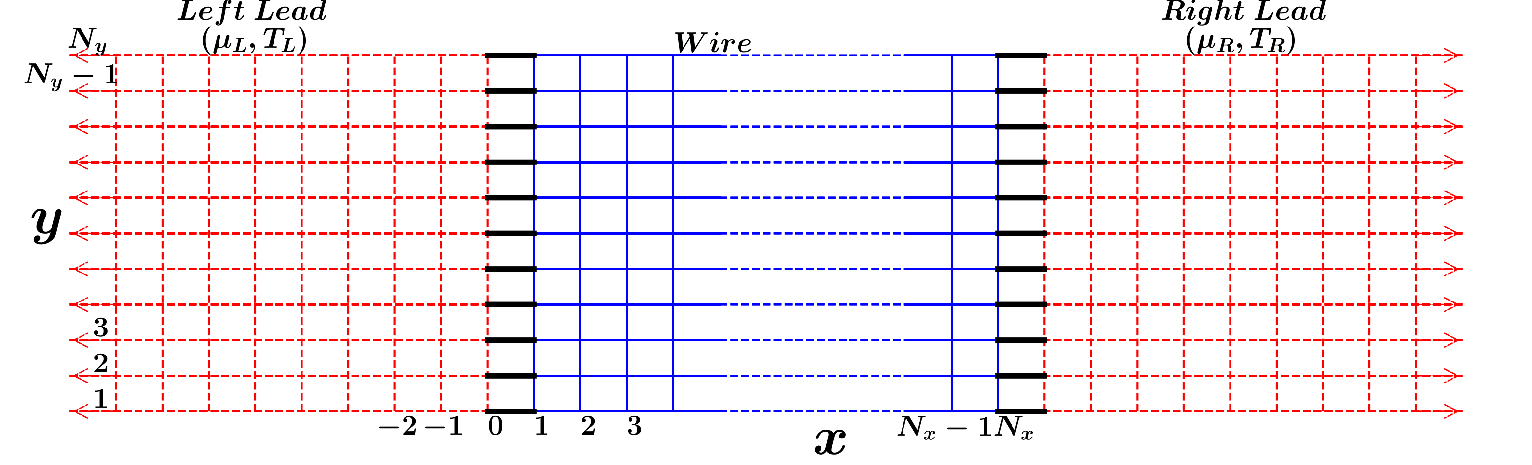
The expressions for the current density can be computed from the correlation matrix, with components given by with and the expectation value is taken in the non-equilibrium steady state. Using NEGF, can be expressed in terms of the effective Green’s function and the Fermi functions of the reservoirs [21].
The NEGF formalism can be reformulated to also compute the current density in the leads. The main idea is to use a setup where we include a part of the leads in the system Hamiltonian (see [21] for details). The current density in any finite segment of the new setup will be identical to the original setup because of uniqueness of the NESS.
As shown in [21], at and in the linear response regime, the current on any bond between sites and , with , , can be written as
| (2) | ||||
| (3) | ||||
| (4) |
where the functions are defined in [21]. We call as the excess current density on the bond and would give the nonequilibrium transport current across the CI. For points in the metal, for any , which implies that . However for points inside the CI, the topological phases support edge currents even in equilibrium, meaning that is non-vanishing on the edges, consequently . This leads to the interesting observation that the excess current density in the CI does not simply change sign when we interchange and (though the total current has this property). Note that the total current across any transverse cross-section vanishes, as expected in equilibrium. We emphasize that the excess current, , is a relatively small correction over , and is the transport current arising due to the chemical potential difference between the reservoirs. Only the total current density is expected to respect the chirality of the Chern insulator, while the excess current density can flow opposite to the chirality of the insulator since it is proportional to . With similar arguments the excess charge density, , where is the charge density for , can be expressed in terms of the correlation matrix (See Eq. (S9) in [21]). We now present numerical results for the conductance and the excess current density profiles.
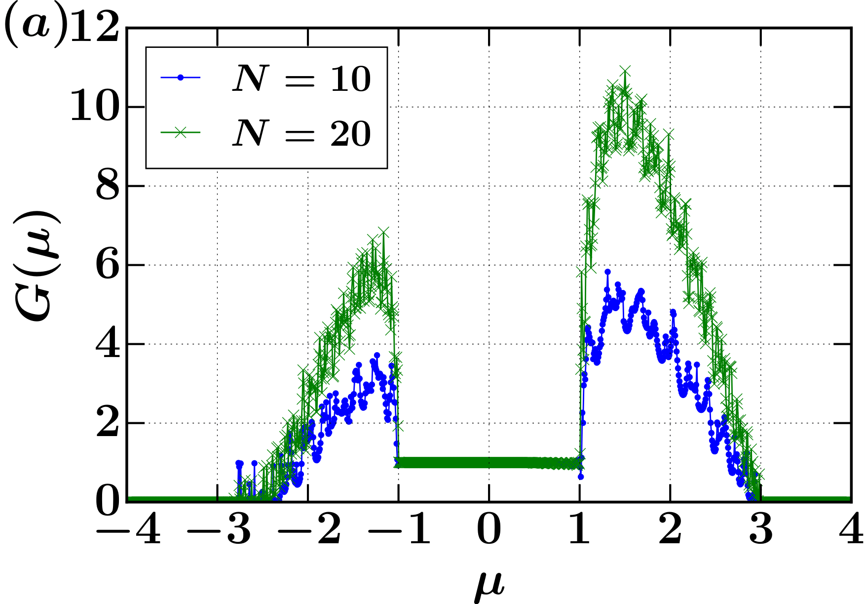
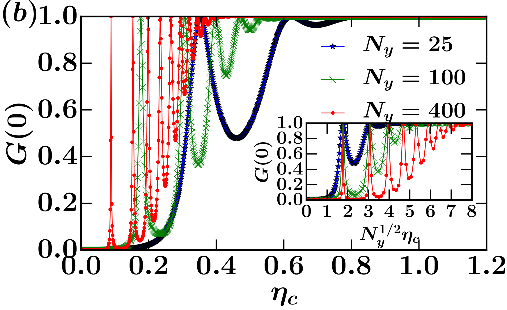
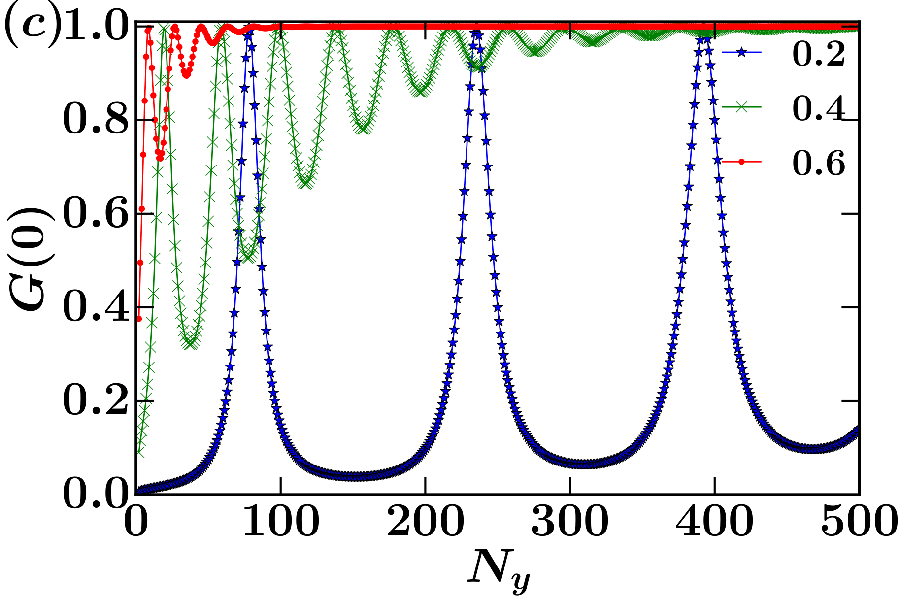
Numerical Results: For the SBHZ wire, the edge modes lie within the gap, we therefore always set to be within the gap of the insulator. In Fig. (2), we plot the conductance as a function of the Fermi level, , for two system sizes. It is seen that when the Fermi level lies in the gap, the value of the conductance (in units of ) is quantized to the value . In Fig. (2b,2c) we show the variation of the conductance, at Fermi level , with the strength of the coupling with the reservoirs, , and the width of the insulator, , respectively. From these plots, we see that the conductance strength approaches the quantized value and eventually becomes independent of and . The approach to the quantized value is oscillatory, with exact quantization being achieved at some specific values of and . The inset of Fig. (2b) shows, remarkably, that the oscillation period scales as .
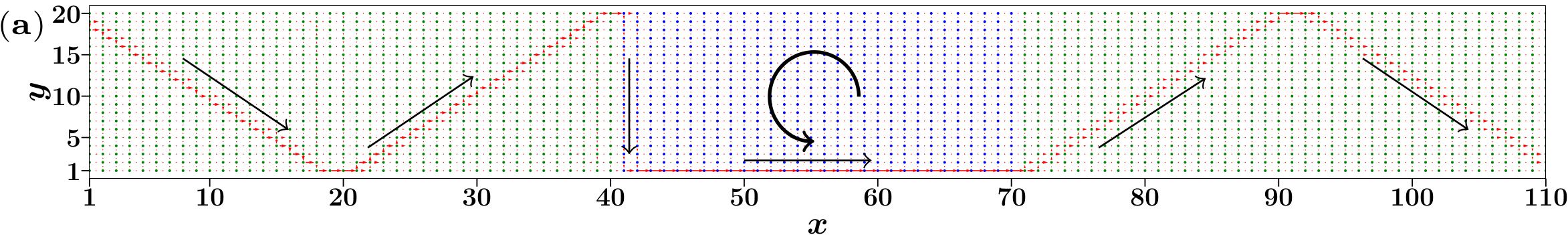
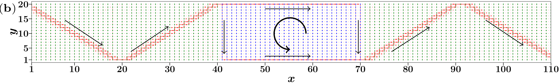
Next, in Fig. (3a), we show the excess current density at zero Fermi level inside the insulator and the normal metallic regions with and . We see that the current flows along the edges of the insulator, and the charge density is also localized along the edges [See Sec. III in [21]], as expected. Surprisingly, the excess current density is sharply localized even in the normal metallic regions. We see that the current primarily flows along the lines at degrees to the horizontal direction and gets multiply reflected until it reaches the top corner of the SBHZ wire. At this corner, it gets injected into the insulator, flows along the edges and then leaves it at the diagonally opposite corner into the normal metallic region on the other end. The current density patterns inside the Chern insulator are sensitive to the choice of and . This is due to that fact that unlike in the metal. We illustrate this in Fig. (3b) which shows the current density pattern for . The current gets injected and ejected from the diagonally opposite corners as in Fig. (3a). However, it now flows along all edges of the CI which is different from Fig. (3a) where it flows only along two of the adjoining edges of the CI. Note that the current density along the opposite edges have opposite chirality, illustrating that the excess current can flow opposite to the chirality of the CI.
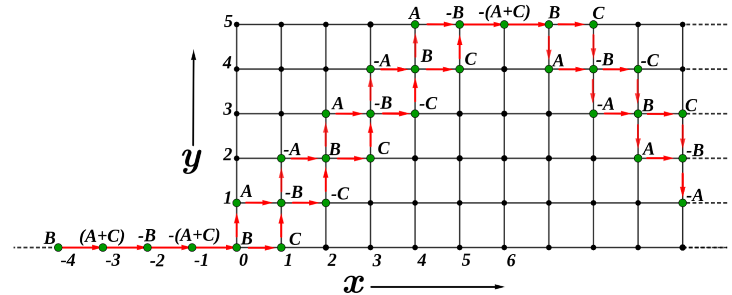
The features of the current density (corner injection and localization in the leads) are sharpest when the Fermi surface of the metal is a square in momentum space and smoothly fade away as the Fermi surface is deformed. In Sec. (IV) of [21], we illustrate this by presenting numerical results of the effects of deforming the Fermi surface on the current density. The fact that the observed localization is sharp at seems to suggest that it is very special to the scattering states formed by the edge modes of the insulator and the reservoir modes at zero energy. At zero energy, the Fermi surface in the metal is a square in momentum space. The localization arises from a particular superposition of the modes on this surface. To illustrate this, consider the setup in Fig. 4 where a current is injected into a semi-infinite metallic strip of width at the left-bottom corner through a point contact with a 1D reservoir. The motivation for considering such a setup comes from the numerical observation (in Fig. (3)) that the current is injected near the corner into the metallic region. For simplicity, let the Hamiltonian of the 1D reservoir and the metallic strip be of the nearest neighbour tight-binding form, with all the hopping parameters, including that of the point contact at the corner, set to . At any lattice site , the wave function components of the nearest neighbour points will sum to zero. In Fig 4, a solution is presented for one such scattering state with the wave function being non-zero only at certain points (large green circles). As , the solution can be written as a simple superposition of states on the square Fermi surface. This state displays a current localization similar to what we see numerically in Fig. (3b). The existence of such states at zero Fermi level and the current injection near the corners are the reasons for the observed localization of the current in the leads. In Sec. (V) of [21] we provide an argument for the observed corner injection/ejection in our numerics. We construct scattering states of the metal-CI junction in the limit and show that there is no injection of current across the junction. Hence we infer that in the strip geometry there can be no injection of current in the bulk but only near the corners.
Topological quantities are expected to be robust to the effects of weak disorder. Hence a natural question to investigate is as to what happens to the current density patterns and the quantized two-terminal conductance on introducing contact disorder. We find features of the current density as well as the quantization are retained in the presence of disorder at the contacts (See Fig. (S6) in [21]).
Conclusion: We looked at electronic transport properties due to the edge modes of a Chern insulator (CI) in the open system geometry using a microscopic approach based on the NEGF formalism, applied to the spinless-BHZ model. We found very nontrivial effects on the current density pattern inside the leads arising from the topology of the insulator. Particularly, our numerical results indicate that the current is highly localized, both in the metal and in the insulator, and the injection (ejection) into (from) the insulator happens only near the corners. The corner injection is robust to contact disorder and changes in the chemical potential. This provides a justification for the main assumption of LB, that of the emergence of an ideal point contact and consequently for the quantization of . By the analysis of scattering states that are formed at metal-CI interfaces we have provided some analytic arguments that support our observations of the current patterns.
We also verified numerically that the two terminal longitudinal conductance in the open geometry is quantized and found very interesting finite-size effects. The conductance, at Fermi level , grows non-monotonically with increasing metal-CI coupling strength, , and increasing transverse system size, . The growth to the quantized value shows oscillations with a period that scales as .
Analytic proofs of the quantization of the two-terminal conductance and the emergence of the ideal point contact for a large class of models of insulators with non-trivial topology is desirable and remains an open problem. This would lead to an understanding of topology of open systems. The experimental observation of the current patterns and the finite size-effects are intriguing possibilites.
We thank Adhip Agarwala, Anindya Das, Sriram Ganeshan, Joel Moore, Arun Paramekanti and Diptiman Sen for helpful discussions. J.M.B and A.D. acknowledge the support of the Department of Atomic Energy, Government of India, under Project No. RTI4001.
References
- Klitzing et al. [1980] K. v. Klitzing, G. Dorda, and M. Pepper, New method for high-accuracy determination of the fine-structure constant based on quantized hall resistance, Phys. Rev. Lett. 45, 494 (1980).
- Thouless et al. [1982] D. J. Thouless, M. Kohmoto, M. P. Nightingale, and M. den Nijs, Quantized hall conductance in a two-dimensional periodic potential, Phys. Rev. Lett. 49, 405 (1982).
- Hatsugai [1993] Y. Hatsugai, Chern number and edge states in the integer quantum hall effect, Phys. Rev. Lett. 71, 3697 (1993).
- Haldane [1988] F. D. M. Haldane, Model for a quantum hall effect without landau levels: Condensed-matter realization of the ”parity anomaly”, Phys. Rev. Lett. 61, 2015 (1988).
- Chang et al. [2013] C.-Z. Chang, J. Zhang, X. Feng, J. Shen, Z. Zhang, M. Guo, K. Li, Y. Ou, P. Wei, L.-L. Wang, et al., Experimental observation of the quantum anomalous hall effect in a magnetic topological insulator, Science 340, 167 (2013).
- Jotzu et al. [2014] G. Jotzu, M. Messer, R. Desbuquois, M. Lebrat, T. Uehlinger, D. Greif, and T. Esslinger, Experimental realization of the topological haldane model with ultracold fermions, Nature 515, 237 (2014).
- Kane and Mele [2005] C. L. Kane and E. J. Mele, topological order and the quantum spin hall effect, Phys. Rev. Lett. 95, 146802 (2005).
- Bernevig et al. [2006] B. A. Bernevig, T. L. Hughes, and S.-C. Zhang, Quantum spin hall effect and topological phase transition in hgte quantum wells, Science 314, 1757 (2006).
- Roy [2009a] R. Roy, classification of quantum spin hall systems: An approach using time-reversal invariance, Physical Review B 79, 195321 (2009a).
- Roy [2009b] R. Roy, Topological phases and the quantum spin hall effect in three dimensions, Physical Review B 79, 195322 (2009b).
- Fu et al. [2007] L. Fu, C. L. Kane, and E. J. Mele, Topological insulators in three dimensions, Phys. Rev. Lett. 98, 106803 (2007).
- Moore and Balents [2007] J. E. Moore and L. Balents, Topological invariants of time-reversal-invariant band structures, Physical Review B 75, 121306 (2007).
- König et al. [2007] M. König, S. Wiedmann, C. Brüne, A. Roth, H. Buhmann, L. W. Molenkamp, X.-L. Qi, and S.-C. Zhang, Quantum spin hall insulator state in hgte quantum wells, Science 318, 766 (2007).
- Hasan and Kane [2010] M. Z. Hasan and C. L. Kane, Colloquium: topological insulators, Rev. Mod. Phys. 82, 3045 (2010).
- Huang and Liu [2018] H. Huang and F. Liu, Quantum spin hall effect and spin bott index in a quasicrystal lattice, Phys. Rev. Lett. 121, 126401 (2018).
- Bandres et al. [2016] M. A. Bandres, M. C. Rechtsman, and M. Segev, Topological photonic quasicrystals: Fractal topological spectrum and protected transport, Phys. Rev. X 6, 011016 (2016).
- Agarwala and Shenoy [2017] A. Agarwala and V. B. Shenoy, Topological insulators in amorphous systems, Phys. Rev. Lett. 118, 236402 (2017).
- Tokura et al. [2017] Y. Tokura, M. Kawasaki, and N. Nagaosa, Emergent functions of quantum materials, Nature Physics 13, 1056 (2017).
- Gusev et al. [2019] G. Gusev, Z. Kvon, E. Olshanetsky, and N. Mikhailov, Mesoscopic transport in two-dimensional topological insulators, Solid State Commun. 302, 113701 (2019).
- Dolcetto et al. [2016] G. Dolcetto, M. Sassetti, and T. L. Schmidt, Edge physics in two-dimensional topological insulators, La Rivista del Nuovo Cimento 39, 113 (2016).
- [21] Supplemental material, URL_will_be_inserted_by_publisher.
- Shankar [2018] R. Shankar, Topological insulators–a review, arXiv preprint arXiv:1804.06471 (2018).
- Dhar and Sen [2006] A. Dhar and D. Sen, Nonequilibrium green’s function formalism and the problem of bound states, Phys. Rev. B 73, 085119 (2006).
- Bhat and Dhar [2020] J. M. Bhat and A. Dhar, Transport in spinless superconducting wires, Phys. Rev. B 102, 224512 (2020).