otherfnsymbols ††‡‡§§¶¶
Hyperspectral photoluminescence and reflectance microscopy of 2D materials
Abstract
Optical micro-spectroscopy is an invaluable tool for studying and characterizing samples ranging from classical semiconductors to low-dimensional materials and heterostructures. To date, most implementations are based on point-scanning techniques, which are flexible and reliable, but slow. Here, we describe a setup for highly parallel acquisition of hyperspectral reflection and photoluminescence microscope images using a push-broom technique. Spatial as well as spectral distortions are characterized and their digital corrections are presented. We demonstrate close-to diffraction-limited spatial imaging performance and a spectral resolution limited by the spectrograph. The capabilities of the setup are demonstrated by recording a hyperspectral photoluminescence map of a CVD-grown MoSe2-WSe2 lateral heterostructure, from which we extract the luminescence energies, intensities and peak widths across the interface.
I Introduction
Optical spectroscopy has proven to be an essential tool in developing the field of two-dimensional semiconductors. Starting with the observation of an indirect-to-direct band gap transition Mak et al. (2010); Splendiani et al. (2010), it has led, among many others, to the observation of the valley-dependent selection rules Cao et al. (2012); Ersfeld et al. (2020), large many-body excitonic states Chen et al. (2018); Ye et al. (2018), excitons in moiré potentials Jin et al. (2019) and magnetic proximity couplings Seyler et al. (2018).
Spectroscopy in the visible and near-infrared spectral region can be performed with sub-micrometer resolution if the light is focused down to (or near) diffraction-limited spots. This is of particular importance for samples with locally varying properties, such as lateral heterojunctions Huang et al. (2014), (gate-defined) nano-scale potentials for exciton confinement Palacios-Berraquero et al. (2017); Thureja et al. (2022), or heterostructures of different materials or stacking orders Bru-Chevallier et al. (2006); Tebbe et al. (2023) as well as for material-specific inhomogeneities, such as strain, charge and screening-induced disorder Shin et al. (2016); Raja et al. (2019); Kolesnichenko et al. (2020) or localized defects He et al. (2015).
To visualize and characterize such features, hyperspectral images, i.e. data cubes that contain data points in two spatial and one spectral dimensions, can be acquired across the entire sample. Most often, this is implemented as point-scanning techniques in which light is focused to a tight spot and scanned across the sample, either by translating the sample with mechanical stages or by moving the focus using galvanic mirrors. While this technique is straight forward to implement, it can become very time-consuming if sample areas are large and need to be scanned at high spatial resolution or if external parameter spaces, such as gate voltages or magnetic fields, are to be varied.
Several pathways exist to increase the speed of the acquisition of hyperspectral images Wang et al. (2017); Candeo et al. (2019). A common approach is to directly image the sample through different (variable) spectral filters. Although this can be a particularly fast method for multi-spectral imaging and works for photoluminescence and absorption imaging, achieving a spectral resolution over a wide range of wavelengths would require a large set of narrow-band filters or a highly tunable filter, which does not induce aberrations. A second approach is to measure several points at a time by using a line of light on the sample and a two-dimensional detector array, such as a CCD or CMOS camera, connected to a spectrometer. This technique requires mechanically scanning the sample in one dimension (also called push-broom), but one naturally achieves a high spectral sampling. While it has been applied to image biological samples in reflection Huebschman et al. (2002); Ortega et al. (2019), these implementations were not designed for conducting different optical experiments, such as photoluminescence spectroscopy, quantitative reflectance measurements or to measure polarization states. The combination of several different experiments, however, is typically needed to obtain a clear picture of the optical transitions and processes in 2D materials Mak et al. (2010); Niehues et al. (2020).
Here, we present a setup for push-broom hyperspectral reflection and photoluminescence (PL) imaging, which is able to acquire hyperspectral images at diffraction-limited performance and a spectral resolution limited by the spectrograph, which can be extended to include polarization optics. We discuss aberrations from the setup and digital image corrections, which allow the use of our setup for quantitative data analysis.
II Setup
The setup presented here is designed to be used for both, white light reflection, as well as for photoluminescence imaging in the visible and near-infrared range (400-800 nm). In both modes, a line-focus is created on the sample. The reflected or emitted light from this line-shaped area is projected onto the entrance slit of an imaging spectrometer. In the spectrometer, this creates a two-dimensional image on the CCD camera, with one dimension corresponding to wavelength and the other corresponding to a spatial dimension. After the acquisition of such an image, the sample is moved along an axis perpendicular to the line-focus by a motorized mechanical stage. An overview of the setup, which is placed on an optical table, is shown in Fig. 1.
The setup is equipped with several light sources, which can be changed using flip mirrors, including a 250 W tungsten-halogen lamp for white light experiments and a 40 mW, 532 nm continuous wave (cw) laser (Thorlabs DJ532-40). The line-focus is created in two different ways for these light sources. Since the white light source is spatially extended, it needs to be spatially filtered in order to achieve a tight focus. In point-scanning setups, this is typically achieved with a pinhole in the common focus plane of two lenses. Here, the pinhole is replaced by a slit of dimension 20 µm 3 mm in between two achromatic doublet lenses. The second lens collimates the white light, which is focused onto the sample using an objective lens. In our setup, several objectives are available, including a 100, NA=0.9 objective. The dimension of the slit and the collimating lens are chosen such that the image of the slit on the sample is just below the resolution limit of the lens. This ensures that the width of the line is as small as it can be while maintaining an intensity high enough for fast image acquisition.
For PL measurements, different laser sources can be employed; here, we use a 532 nm continuous wave (cw) laser (Thorlabs DJ532-40). It is first expanded to exceed the dimension of the back aperture of the microscope objective. The laser beam is then passed through a cylindrical lens (, 40 cm), which is placed in front of the beam splitter, at a distance of approximately in front of the microscope objective. As the objective only focuses the collimated dimension, a line-focus is generated on the sample plane.
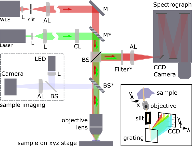
The reflected or emitted light from the line-shaped area on the sample is collected and collimated by the objective. It is then split from the incoming light path by a non-polarizing beam slitter and imaged onto the slit of the imaging spectrometer (Andor Shamrock 500i with gratings of 150, 300 and 600l/mm) by an achromatic lens ( 15 cm). Optional filters or polarization optics can be introduced in front of the focusing lens. Inside the spectrometer, the line is split into its wavelengths by the grating, creating a two-dimensional image on the CCD camera (Andor Newton DU920P-BEX2-DD). The vertical-direction of the CCD-images corresponds to a real-space y-dimension, and the horizontal-direction to a wavelength-space -dimension.
Finally, a hyperspectral data cube is recorded by moving the sample by a motorized xyz stage perpendicular to the long focus direction while taking spectral images at each position (x and y motors: PI V-408, z stage: Newport M-MVN80 with TRA25PPD actuator). Since some level of chromatic aberration exists in the setup, the raw images need to be digitally corrected before the data can be analyzed.
For alignment purposes, both the sample and the focus can be viewed simultaneously using an imaging setup. This imaging module consists of a lighting arm with an LED Light Source (Thorlabs, MNWHL4) and an aspheric collimation lens, a beam splitter, and the imaging arm with a digital color camera (The imaging source, DFK 33UX265) and an achromatic tube lens ( 10 cm). The imaging setup is introduced into the beam path with a pellicle beam splitter, which keeps the offset of the light sources on the sample to a minimum.
III Image analysis
III.1 Chromatic aberrations
Due to the use of refractive optics, some level of chromatic aberration is present in the setup. This aberration manifests mainly as a wavelength dependence of the spatial dimension on the CCD camera of the imaging spectrometer.
To visualize the distortions, we take white light reflectance images from a calibration sample of micro-patterned stripes of 5/50 nm thick Cr/Au with 0.8 µm width and unequal spacing, fabricated on Si/SiO2. Fig. 2 a shows a microscope image of the white light line-focus on this sample. The corresponding spectral image, taken with the spectrograph, is shown in Fig. 2 b. The vertical direction corresponds to the spatial dimension along the line-focus. Since gold has a higher reflectance than Si/SiO2 across this wavelength range, it appears as bright lines in the spectral dimension.
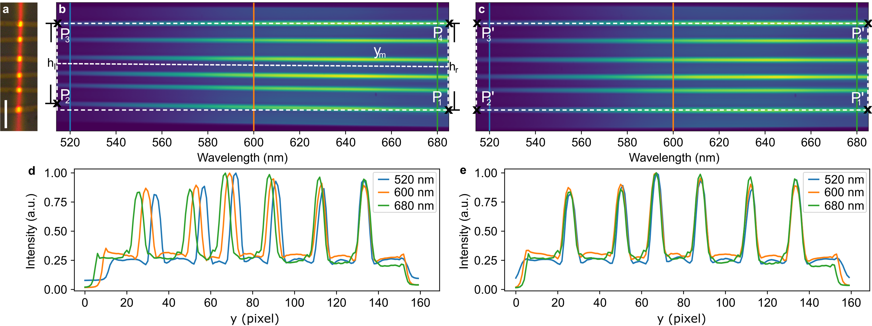
The lines in the spectral image are tilted, which is also seen in the different sizes of the vertical cuts at three different wavelengths, plotted in Figure 2 d. These distortions need to be corrected in order to retrieve the actual reflectance (or photoluminescence) spectra at each spatial point from horizontal cuts of the image.
To quantify the distortions, we first find four coordinates in the image, which correspond to two spatial points on the sample at two different wavelengths. As the wavelength axis is aberration corrected by the spectrograph, and . The y-coordinates can be found from the vertical line cuts, e.g. by the intensity maximum of the topmost and bottom-most gold feature as shown in Fig. 2 d. We find that the distortions can be well approximated to be linear in wavelength, so that the four coordinates generally lie on a (nonsymmetric) trapezoid. In the corrected image, these four coordinates need to form a rectangle, i.e. and .
For the image transformation, we work backwards, starting from a regular rectangular grid into which the raw data is supposed to be transformed. This grid is squeezed and sheared in y-direction to match the shape of the trapezoid, creating a grid of unequal spacing, but of the same amount of points at each wavelength. The intensities of the measured image are then interpolated at the positions of this grid. If displayed as an array of equally spaced pixels, this grid corresponds to the corrected image. Importantly, this transformation is different from an affine transform, as the x direction (wavelength) is not modified in this transformation.
The transformation of the rectangular grid is performed in the following way: first, the grid points are squeezed in y-direction by a factor . Using the side lengths and , the squeezing factor is given by:
| (1) |
Secondly, it is sheared such that the center line matches the middle line of the distorted image . The position of the middle line is a linear function, given by the middle heights on each side and :
| (2) |
The coordinates of each pixel on the distorted grid, , are then given in terms of the positions on the rectangular grid, , by:
| (3) |
The interpolation of the image onto these coordinates is implemented using the remap function of the python package OpenCV. The resulting image and line cuts are shown in Fig. 2 c and e. A horizontal line cut now corresponds to the reflected spectrum at one particular spatial point. The transformation is generally applied to all images before further analysis. A new calibration must be performed after each major realignment of the setup.
III.2 Intensity profiles
Images of the line-foci as well as their spatial profiles along the x and y directions are shown in Fig. 3. Along the long dimension (x-direction), the white light intensity is relatively flat over several tens of micrometers, but contains some features. The laser has an almost Gaussian shape with a full width at half maximum (FWHM) of 16 µm. These profiles directly result from the different ways the lines are achieved: as the intensity along the slit is homogeneous, so is the resulting focus, whereas the profile of the laser originates from the Gaussian shape of the collimated laser beam. Note that using a slit in the collimated laser beam instead of a cylindrical lens does not yield a more homogeneous intensity profile along the long direction, but rather leads to fringes due to diffraction Luo et al. (2015).
For a quantitative analysis of the data, the varying intensity of both white light and laser needs to be taken into account. In white light experiments, one often determines the reflection contrast, i.e. the reflected intensity on the sample divided by the intensity next to the sample. This eliminates the parameters of the setup, such as the emission spectrum of the lamp and sensitivity curve of the detector. It is possible, as the intensity of the light is typically low enough to neglect nonlinear effects. Using the push-broom technique introduced here, the reflection contrast can either be calculated taking a reference on a single point, which introduces a small error due to the remaining fluctuations of the white light. It is therefore favorable to use an entire reference line, which further eliminates these variations (see Supplementary Information for details on the implementation).
For photoluminescence experiments, the excitation power varies to a larger degree due to the profile of the laser. By taking a reference measurement of the laser intensity on the CCD of the spectrograph (or the PL intensity of a homogeneous test sample), it can nevertheless be accounted for. In this case, each row of the acquired data images is divided by the (normalized) intensity of the reference measurement. Note that this approach requires that the PL intensity be linearly dependent on the excitation power. Although this holds well, for example for neutral excitons in transition metal dichalcogenides (TMDs), it might not for the emission of other states, such as from localized defects Tongay et al. (2013) or biexcitons Ye et al. (2018); Chen et al. (2018). To study states with a nonlinear excitation dependence with the push-broom technique, the intensity in the y direction would need to be homogenized, e.g. by the use of a top-hat beam shaper or by selecting only a small fraction of the line. In order to stay within reasonable variations of excitation density, we typically truncate the PL images at approximately 50% of the maximum laser intensity and apply the intensity correction to all images.
IV Resolution of the setup
We now discuss the performance of the setup. The spatial resolution perpendicular to the line-focus is trivially given by the width of the line-focus (see Fig. 3 b). In this dimension (x-direction), we measure a FWHM of 0.40 µm for the white light source (spectrally filtered at nm) and 0.31 µm for the 532 nm laser. The slightly smaller width of the laser is likely related to the different beam profiles and the shorter wavelength of the laser beam.
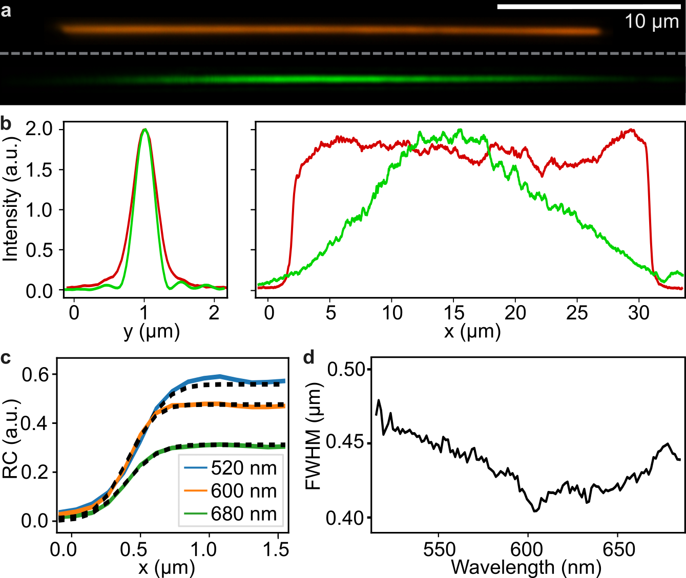
To verify that the spatial resolution in the direction parallel to the line is comparable to the FWHM in perpendicular direction, we performed knife-edge measurements, in which the white light focus is placed over the edge of a trilayer graphene flake. The measured spectral image is analyzed by taking vertical cuts at each wavelength. Three examples of these cuts are shown in Fig. 3 d. They are analyzed by fitting an error-function to the data; the resulting FWHM corresponds to the spatial resolution of the setup and is shown in Fig. 3 d). At 620 nm, the spatial resolution is indeed similar to the measured FWHM in the perpendicular direction. While the spatial resolution varies with wavelength, this is not a feature of the line-focus. It results from the chromatic aberration of the lenses used in the setup and would also be present in point-scanning techniques. The wavelength of the best (i.e. diffraction-limited) spatial resolution can be adjusted by changing the position of the last focusing lens before the spectrometer.
The spectral resolution of our setup is given by the resolution of the spectrograph. Due to the use of curved mirrors with an aberration corrected shape, it does not significantly vary with the y position (see the datasheet of the manufacturer). Using the grating with the highest groove density, the spectral resolution is on the order of 0.15 nm.
V PL imaging of lateral heterostructures

We demonstrate the capability of the setup by acquiring a hyperspectral photoluminescence and reflection contrast image of a TMD monolayer sample at room temperature; further reflection contrast measurements taken with the setup can be found in the study of Ref. Tebbe et al. (2023). The sample is a MoSe2-WSe2 in-plane heterostructure grown by chemical vapor deposition using the one-pot chemical vapor deposition growth method Sahoo et al. (2018). A micrograph of the sample is shown in Fig. 4 a.
Spectral images were taken with a laser power of 130 µW (nm), which translates to an irradiance of approximately 3 µW/µm2 (note that the data were taken with a different cylindrical lens, which led to a laser profile of 7 µm FWHM). To map the entire flake, 5 rows of 175 spectral images were taken, with step sizes of 7 µm in the y direction and 0.2 µm in the x direction. Note that the step size in the x-direction is chosen to match the real-space pitch in the y-direction on the CCD, such that the images appear without distortions. Each image had an exposure time of 4 s and the total time to acquire all data, corresponding to 49000 individual spectra, was 75 min. The 15 minutes not connected to data acquisition are linked to the communication with the camera and the moving of the mechanical stages.
The raw images are first corrected for chromatic aberration and excitation power as described in the previous sections. Afterwards, the five rows are stitched together and averaged where they overlap (see SI1 for details). A background spectrum is subtracted by averaging an area without sample (see SI2 for details of background and reference spectra). A false-color image of the hyperspectral data is shown in Fig. 4 b, where the color channels are the integrated counts (normalized to their respective maximum) in the spectral range between 1.46 to 1.54 eV (red) and 1.56 to 1.64 eV (blue). All major features seen in the micrograph can be identified (e.g. the thicker area in the middle), and the PL image appears without visible distortions. Note that the WSe2 areas appear purple, as the tail of the luminescence of WSe2 reaches into the lower-energy integration window.
In Fig. 4 c, a subset of the spectra of the data set are shown, extracted along a line perpendicular to the MoSe2-WSe2 interface (see the white arrow in Fig. 4 b). In both, MoSe2 and WSe2 regions, the PL emission shows a single peak, which is slightly asymmetric in the WSe2 region. The intensity of MoSe2 is significantly lower than that of WSe2, which has been attributed to the different ordering of bright and dark states in the two materials Wang et al. (2015); Zhang et al. (2015).
For a more quantitative analysis of the data, we fit the spectra with two Gaussian peaks. The resulting peak-heights across the interface are shown in the inset of Fig. 4 c. The dashed line indicates the interface between the two materials as seen in the optical microscope image. The most striking feature is that, while the intensity of WSe2 drops right at the interface, the intensity of MoSe2 is strongly reduced within a distance of approximately one micrometer from the interface. The drop in intensity towards the interface could be caused by a higher defect density at the interface or by diffusion and charge carrier transfer to the WSe2 side Berweger et al. (2020); Jia et al. (2020); Ambardar et al. (2022); Shimasaki et al. (2022); Beret et al. (2022). At the used irradiance of 3 µW/µm2, a reduction of PL due to exciton-exciton annihilation is not expected Lee et al. (2018).
The peak positions and widths of the entire sample are also determined by the fit and are color-coded in Fig. 4 d and e. Both peak energies are redshifted compared to literature values, indicating tensile strain across the entire sample Island et al. (2016); Aslan et al. (2018), which is common for CVD grown materials on silica Ahn et al. (2017). Both the peak position and the width show variations of few meV across the respective materials. The most obvious feature in the WSe2 is the shift towards higher peak energy and higher peak width at the corners of the triangle, which hints towards reduced tensile strain at the corners Aslan et al. (2018); Niehues et al. (2018). In the MoSe2 area, a systematic change of the peak width can be observed, with the peaks getting narrower toward the outside, which points to a greater strain towards the interface Niehues et al. (2018).
VI Conclusion and outlook
In conclusion, we implemented and characterized a hyperspectral push-broom micro-spectroscopy setup for highly parallel acquisition of reflection and photoluminescence spectra. To demonstrate the capabilities, we measured the PL spectra of a two-dimensional lateral heterostructure sample.
The implementation of the parallel measurement scheme presented here can easily be implemented in existing setups and can be combined with various measurement techniques. By inserting polarization optics, the setup can be used to map e.g. the polarization-resolved luminescence connected to the valley selection rules of TMDs Zeng et al. (2012); Mak et al. (2012), or the magnetic circular dichroism in 2D heterostructures including magnetic materials Zhong et al. (2017); Seyler et al. (2018). The concept can also be applied for Raman imaging, if a laser of sufficiently narrow line width in combination with appropriate filters is used and to other measurement techniques relevant to the semiconductor industry, such as optical critical dimension methods Hoobler and Apak (2003). Lastly, the setup can be modified to use reflective optics for a more broadband operation, potentially ranging from the infrared to the UV spectral region Ma et al. (2020).
The measurement scheme has broad applicability in studying quantitative optical properties of two-dimensional materials and beyond. It is particularly useful for imaging experiments of large sample areas or in situations in which multi-dimensional parameters scans are to be combined with high-resolution imaging.
Supplementary Material
See the supplementary material for details on how multiple passes are stitched together and how background and reference spectra are extracted from the hyperspectral images, i.e. datacubes.
Data availability statement
The data that support the findings of this study are openly available in zenodo, at doi.org/10.5281/zenodo.7924667.
Acknowledgments
This project has received funding from the European Union’s Horizon 2020 research and innovation program under grant agreement No. 881603 (Graphene Flagship). PKS acknowledges the Department of Science and Technology (DST), India (Project Code: DST/TDT/AMT/2021/003 (G)&(C)).
References
References
- Mak et al. (2010) K. F. Mak, C. Lee, J. Hone, J. Shan, and T. F. Heinz, Phys. Rev. Lett. 105, 136805 (2010).
- Splendiani et al. (2010) A. Splendiani, L. Sun, Y. Zhang, T. Li, J. Kim, C. Y. Chim, G. Galli, and F. Wang, Nano Letters 10, 1271 (2010).
- Cao et al. (2012) T. Cao, G. Wang, W. Han, H. Ye, C. Zhu, J. Shi, Q. Niu, P. Tan, E. Wang, B. Liu, and J. Feng, Nature communications 3, 887 (2012).
- Ersfeld et al. (2020) M. Ersfeld, F. Volmer, L. Rathmann, L. Kotewitz, M. Heithoff, M. Lohmann, B. Yang, K. Watanabe, T. Taniguchi, L. Bartels, J. Shi, C. Stampfer, and B. Beschoten, Nano Letters 20, 3147 (2020).
- Chen et al. (2018) S. Y. Chen, T. Goldstein, T. Taniguchi, K. Watanabe, and J. Yan, Nature Communications 9, 3717 (2018).
- Ye et al. (2018) Z. Ye, L. Waldecker, E. Y. Ma, D. Rhodes, A. Antony, B. Kim, X.-X. Zhang, M. Deng, Y. Jiang, Z. Lu, D. Smirnov, K. Watanabe, T. Taniguchi, J. Hone, and T. F. Heinz, Nature Communications 9, 3718 (2018).
- Jin et al. (2019) C. Jin, E. C. Regan, A. Yan, M. I. B. Utama, D. Wang, S. Zhao, Y. Qin, S. Yang, Z. Zheng, S. Shi, K. Watanabe, T. Taniguchi, S. Tongay, A. Zettl, and F. Wang, Nature 567, 76 (2019).
- Seyler et al. (2018) K. L. Seyler, D. Zhong, B. Huang, X. Linpeng, N. P. Wilson, T. Taniguchi, K. Watanabe, W. Yao, D. Xiao, M. A. McGuire, K. M. C. Fu, and X. Xu, Nano Letters 18, 3823 (2018).
- Huang et al. (2014) C. Huang, S. Wu, A. M. Sanchez, J. J. P. Peters, R. Beanland, J. S. Ross, P. Rivera, W. Yao, D. H. Cobden, and X. Xu, Nature Materials 13, 1096 (2014).
- Palacios-Berraquero et al. (2017) C. Palacios-Berraquero, D. M. Kara, A. R. Montblanch, M. Barbone, P. Latawiec, D. Yoon, A. K. Ott, M. Loncar, A. C. Ferrari, and M. Atatüre, Nature Communications 8, 15093 (2017).
- Thureja et al. (2022) D. Thureja, A. Imamoglu, T. Smoleński, I. Amelio, A. Popert, T. Chervy, X. Lu, S. Liu, K. Barmak, K. Watanabe, T. Taniguchi, D. J. Norris, M. Kroner, and P. A. Murthy, Nature 606, 298 (2022).
- Bru-Chevallier et al. (2006) C. Bru-Chevallier, H. Chouaib, A. Bakouboula, and T. Benyattou, Applied Surface Science 253, 194 (2006).
- Tebbe et al. (2023) D. Tebbe, M. Schütte, K. Watanabe, T. Taniguchi, C. Stampfer, B. Beschoten, and L. Waldecker, npj 2D Materials and Applications 7, 29 (2023).
- Shin et al. (2016) B. G. Shin, G. H. Han, S. J. Yun, H. M. Oh, J. J. Bae, Y. J. Song, C. Y. Park, and Y. H. Lee, Advanced Materials 28, 9378 (2016).
- Raja et al. (2019) A. Raja, L. Waldecker, J. Zipfel, Y. Cho, S. Brem, J. D. Ziegler, M. Kulig, T. Taniguchi, K. Watanabe, E. Malic, T. F. Heinz, T. C. Berkelbach, and A. Chernikov, Nature Nanotechnology 14, 832 (2019).
- Kolesnichenko et al. (2020) P. V. Kolesnichenko, Q. Zhang, T. Yun, C. Zheng, M. S. Fuhrer, and J. A. Davis, 2D Materials 7, 025008 (2020).
- He et al. (2015) Y. M. He, G. Clark, J. R. Schaibley, Y. He, M. C. Chen, Y. J. Wei, X. Ding, Q. Zhang, W. Yao, X. Xu, C. Y. Lu, and J. W. Pan, Nature Nanotechnology 10, 497 (2015).
- Wang et al. (2017) Y. W. Wang, N. P. Reder, S. Kang, A. K. Glaser, and J. T. Liu, Nanotheranostics 1, 369 (2017).
- Candeo et al. (2019) A. Candeo, B. E. Nogueira de Faria, M. Erreni, G. Valentini, A. Bassi, A. M. de Paula, G. Cerullo, and C. Manzoni, APL Photonics 4, 120802 (2019).
- Huebschman et al. (2002) M. Huebschman, R. Schultz, and H. Garner, IEEE Engineering in Medicine and Biology Magazine 21, 104 (2002).
- Ortega et al. (2019) S. Ortega, R. Guerra, M. Diaz, H. Fabelo, S. Lopez, G. M. Callico, and R. Sarmiento, IEEE Access 7, 122473 (2019).
- Niehues et al. (2020) I. Niehues, P. Marauhn, T. Deilmann, D. Wigger, R. Schmidt, A. Arora, S. Michaelis De Vasconcellos, M. Rohlfing, and R. Bratschitsch, Nanoscale 12, 20786 (2020).
- Luo et al. (2015) Z. Luo, J. Maassen, Y. Deng, Y. Du, R. P. Garrelts, M. S. Lundstrom, P. D. Ye, and X. Xu, Nat. Commun. 6, 1 (2015).
- Tongay et al. (2013) S. Tongay, J. Suh, C. Ataca, W. Fan, A. Luce, J. S. Kang, J. Liu, C. Ko, R. Raghunathanan, J. Zhou, F. Ogletree, J. Li, J. C. Grossman, and J. Wu, Scientific Reports 3, 2657 (2013).
- Sahoo et al. (2018) P. K. Sahoo, S. Memaran, Y. Xin, L. Balicas, and H. R. Gutiérrez, Nature 553, 63 (2018).
- Wang et al. (2015) G. Wang, C. Robert, A. Suslu, B. Chen, S. Yang, S. Alamdari, I. C. Gerber, T. Amand, X. Marie, S. Tongay, and B. Urbaszek, Nature Communications 6, 10110 (2015).
- Zhang et al. (2015) X. X. Zhang, Y. You, S. Y. F. Zhao, and T. F. Heinz, Physical Review Letters 115, 257403 (2015).
- Berweger et al. (2020) S. Berweger, H. Zhang, P. K. Sahoo, B. M. Kupp, L. Blackburn, E. M. Miller, T. M. Wallis, D. V. Voronine, P. Kabos, and S. U. Nanayakkara, ACS Nano 14, 14080 (2020).
- Jia et al. (2020) S. Jia, Z. Jin, J. Zhang, J. Yuan, W. Chen, W. Feng, P. Hu, P. M. Ajayan, and J. Lou, Small 16, 2002263 (2020).
- Ambardar et al. (2022) S. Ambardar, R. Kamh, Z. H. Withers, P. K. Sahoo, and D. V. Voronine, Nanoscale 14, 8050 (2022).
- Shimasaki et al. (2022) M. Shimasaki, T. Nishihara, K. Matsuda, T. Endo, Y. Takaguchi, Z. Liu, Y. Miyata, and Y. Miyauchi, ACS Nano 16, 8205 (2022).
- Beret et al. (2022) D. Beret, I. Paradisanos, H. Lamsaadi, Z. Gan, E. Najafidehaghani, A. George, T. Lehnert, J. Biskupek, U. Kaiser, S. Shree, A. Estrada-Real, D. Lagarde, X. Marie, P. Renucci, K. Watanabe, T. Taniguchi, S. Weber, V. Paillard, L. Lombez, J. M. Poumirol, A. Turchanin, and B. Urbaszek, npj 2D Materials and Applications 6, 84 (2022).
- Lee et al. (2018) Y. Lee, G. Ghimire, S. Roy, Y. Kim, C. Seo, A. K. Sood, J. I. Jang, and J. Kim, ACS Photonics 5, 2904 (2018).
- Island et al. (2016) J. O. Island, A. Kuc, E. H. Diependaal, R. Bratschitsch, H. S. Van Der Zant, T. Heine, and A. Castellanos-Gomez, Nanoscale 8, 2589 (2016).
- Aslan et al. (2018) O. B. Aslan, M. Deng, and T. F. Heinz, Physical Review B 98, 115308 (2018).
- Ahn et al. (2017) G. H. Ahn, M. Amani, H. Rasool, D. H. Lien, J. P. Mastandrea, J. W. Ager, M. Dubey, D. C. Chrzan, A. M. Minor, and A. Javey, Nature Communications 8, 608 (2017).
- Niehues et al. (2018) I. Niehues, R. Schmidt, M. Drüppel, P. Marauhn, D. Christiansen, M. Selig, G. Berghäuser, D. Wigger, R. Schneider, L. Braasch, R. Koch, A. Castellanos-Gomez, T. Kuhn, A. Knorr, E. Malic, M. Rohlfing, S. Michaelis De Vasconcellos, and R. Bratschitsch, Nano Letters 18, 1751 (2018).
- Zeng et al. (2012) H. Zeng, J. Dai, W. Yao, D. Xiao, and X. Cui, Nature nanotechnology 7, 490 (2012).
- Mak et al. (2012) K. F. Mak, K. He, J. Shan, and T. F. Heinz, Nature Nanotechnology 7, 494 (2012).
- Zhong et al. (2017) D. Zhong, K. L. Seyler, X. Linpeng, R. Cheng, N. Sivadas, B. Huang, E. Schmidgall, T. Taniguchi, K. Watanabe, M. A. McGuire, W. Yao, D. Xiao, K. M. C. Fu, and X. Xu, Science Advances 3, e1603113 (2017).
- Hoobler and Apak (2003) R. J. Hoobler and E. Apak, 23rd Annual BACUS Symposium on Photomask Technology 5256, 638 (2003).
- Ma et al. (2020) E. Y. Ma, L. Waldecker, D. Rhodes, J. Hone, K. Watanabe, T. Taniguchi, and T. F. Heinz, Review of Scientific Instruments 91, 073107 (2020).