Atomic-layer controlled THz Spintronic emission from Epitaxially grown Two dimensional PtSe2/ferromagnet heterostructures
Abstract
Terahertz (THz) Spintronic emitters based on ferromagnetic/metal junctions have become an important technology for the THz range, offering powerful and ultra-large spectral bandwidths. These developments have driven recent investigations of two-dimensional (2D) materials for new THz spintronic concepts. 2D materials, such as transition metal dichalcogenides (TMDs), are ideal platforms for SCC as they possess strong spin-orbit coupling (SOC) and reduced crystal symmetries. Moreover, SCC and the resulting THz emission can be tuned with the number of layers, electric field or strain. Here, epitaxially grown 1T-PtSe2 and sputtered Ferromagnet (FM) heterostructures are presented as a novel THz emitter where the 1T crystal symmetry and strong SOC favor SCC. High quality of as-grown PtSe2 layers is demonstrated and further FM deposition leaves the PtSe2 unaffected, as evidenced with extensive characterization. Through this atomic growth control, the unique thickness dependent electronic structure of PtSe2 allows the control of the THz emission by SCC. Indeed, we demonstrate the transition from the inverse Rashba-Edelstein effect in one monolayer to the inverse spin Hall effect in multilayers. This band structure flexibility makes PtSe2 an ideal candidate as a THz spintronic 2D material and to explore the underlying mechanisms and engineering of the SCC for THz emission.
I Introduction
During the past two decades, two-dimensional (2D) materials have raised tremendous interest in the scientific community for the novel and specific properties as a result of their reduced dimensionality and van der Waals character [1, 2, 3]. In particular, when isolated to one monolayer (ML), transition metal dichalcogenides (TMD) 1H-MX2 (with M=Mo, W and X=S, Se) become direct bandgap semiconductors with remarkable optical properties [4, 5]. In addition, inversion symmetry breaking giving rise to in-plane electric field combined with strong spin-orbit coupling gives rise to two inequivalent K valleys exhibiting spin-valley locking [6]. This property is at the origin of unique phenomena such as optical valley selection by circularly polarized light [7], large valley Hall and Nernst effects [8, 9], anisotropic spin relaxation [10] and sizeable spin-orbit torques [11]. Platinum diselenide (PtSe2) is a recent TMD that shows several key properties like air stability [12], high carrier mobility [13], high photoelectrical response in the near-infrared range [14] and defect-induced ferromagnetism [15]. By selectively substituting selenium by sulfur atoms, the polar SePtS Janus material could also be synthesized [16]. Moreover, it exhibits a layer-dependent bandgap: one monolayer of PtSe2 is a 1.9 eV bandgap semiconductor while for layers greater than 3 ML it becomes semi-metallic [17]. Finally, owing to the large atomic weight of platinum, PtSe2 possesses the greatest spin-orbit coupling among transition metal diselenides making it an excellent candidate to study spin-to-charge conversion (SCC) in van der Waals materials. In this respect, it constitutes a unique system to observe the transition from inverse Rashba-Edelstein effect (IREE) in the semiconducting phase to inverse spin Hall effect (ISHE) in the semi-metallic phase. Furthermore, 1T-PtSe2 shows crystal inversion symmetry favoring in-plane spin textures at interfaces whereas spins are mostly locked out-of-plane in 1H-MX2 preventing SCC for in-plane polarized spin currents. Angle and spin-resolved photoemission spectroscopy measurements have indeed demonstrated the existence of in-plane helical spin textures in the valence band of monolayer PtSe2 [18, 19]. To study SCC in 2D materials, spin pumping is typically used and has, for example, been used to measure the strength of IREE [20]. On the other hand, Terahertz (THz) emission spectroscopy has become a powerful and established tool to probe SCC [21, 22]. The associated devices are known as spintronic THz emitters and were first demonstrated with metallic ferromagnetic (Co, Fe…)/nonmagnetic (Pt, W…) thin films [23, 24, 25]. They present several advantages compared to other THz sources such as broadband THz emission, high efficiency and easy control of radiation parameters. To date, very few 2D materials have been incorporated in THz spintronic emitters [26, 27, 28, 29] and they all exhibit the 1H crystal structure which is not favorable to convert in-plane polarized spins into charge currents. Indeed, the combination of inversion symmetry breaking and strong SOC forces the spin of electrons with finite momentum to be out-of-plane. In this work, we have grown single crystalline mono and multilayers of 1T-PtSe2 on graphene by van der Waals epitaxy [30, 31, 32, 33] and developed a soft sputtering process to grow amorphous CoFeB on top of PtSe2 obtaining atomically sharp CoFeB/PtSe2 interface. We used a full set of characterization tools to demonstrate the structural and chemical preservation of PtSe2 after CoFeB deposition. SCC was then studied on these advanced 2D samples as a function of PtSe2 thickness from 1 to 15 ML using THz emission spectroscopy that showed the efficient generation of THz electric fields through SCC. This THz emission is shown to arise from the 1T crystal structure and large spin-orbit coupling of PtSe2. Indeed, negligible signals were obtained for 1T-VSe2 with low spin-orbit coupling and for 1H-WSe2 with 1H crystal structure. Further, the THz electric field clearly shows a two-step dependence on the PtSe2 thickness that we interpret as the transition from the IREE in the semiconducting regime to the ISHE in the semimetallic regime. As shown by ab initio calculations, the IREE arises from the large Rashba spin splitting at the PtSe2/graphene interface by the combination of large spin-orbit coupling and the interfacial electric dipole. By fitting the thickness dependence, we could extract the out-of-plane spin diffusion length in PtSe2 to be 2-3 nm and found that SCC by IREE at the PtSe2/Gr interface is twice as efficient than that of ISHE in bulk PtSe2. For its unique thickness dependent electronic structure, PtSe2 spintronic structures enable to observe the transition from IREE to ISHE and opens up perspectives for the application of these structures to THz spintronics. Furthermore, by adjusting the Fermi level position via gating the material, it will be possible to modulate and dramatically enhance the SCC efficiency and achieve further large enhancement of the spintronic THz emission.
II Results and discussion
II.1 Sample growth and characterization
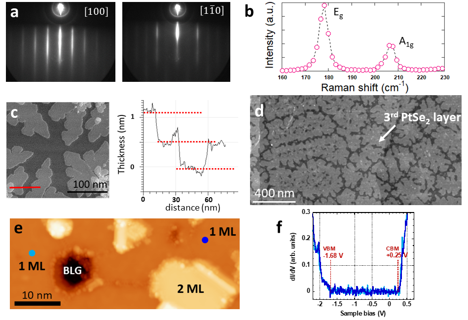
All the samples are grown under ultra-high vacuum (UHV) conditions in the low 10-10 mbar pressure range. Substrates are epitaxial graphene on undoped SiC(0001) thermally prepared by surface graphitization [34, 35]. The low spin-orbit interaction in graphene and SiC ensures negligible SCC. Prior to the growth, the substrates are annealed at 800°C during 30 minutes under UHV to desorb contaminants. The substrate is then maintained at 300°C during the growth. Platinum is evaporated using an electron gun at a constant rate of 0.003125 Å/s for 1 ML PtSe2 and 0.00625 Å/s for the other thicknesses as monitored by a quartz microbalance. Selenium is evaporated using a Knudsen cell with a vapor pressure of 10-6 mbar at the sample position. This ensures a large Se:Pt ratio greater than 10 necessary to avoid the formation of Se vacancies in the material. Up to 3 ML of PtSe2, the growth is performed in this one step whilst for thicker films, it is achieved in several steps alternating deposition and annealing at 700°C under Se to smooth out the surface. At the end of the growth, all the films are annealed at 700°C during 15 minutes to improve the crystal quality. PtSe2 grows epitaxially on graphene and typical reflection high energy electron diffraction patterns (RHEED) are shown in Fig. 1a along two azimuths 30° apart from each other. The observed thin streaks and anisotropic character demonstrate the high crystalline quality of PtSe2 films, i.e. large grain size and good crystalline orientation. As usually observed in van der Waals epitaxy of 2D materials on graphene, the mosaic spread measured by azimuthal in-plane x-ray diffraction shows a maximum of 5° [30]. Thanks to the air stability of PtSe2, it is possible to perform ex-situ characterization. The Raman spectrum (see Experimental section) for 10 ML of PtSe2 is shown in Fig. 1b. We clearly distinguish the two characteristic vibration modes of PtSe2 Eg (in-plane) at 177.9 cm-1 and A1g (out-of-plane) at 206.9 cm-1 with typical full width at half maximum (FWHM) of 4 cm-1 [36]. Atomic force microscopy (AFM) images performed on less than 1 and 3 ML are shown in Fig. 1c and 1d, respectively. For partially covered graphene in Fig. 1c, the height profile gives identical PtSe2/Gr and PtSe2/PtSe2 step heights of 0.5 nm corresponding to the c-lattice parameter of bulk PtSe2. Moreover, for 3 ML in Fig. 1d, the AFM image illustrates the quasi completion (96.6 %) of the third layer and the layer-by-layer film growth. This growth mode allows for the fine control of the number of deposited PtSe2 monolayers.
Scanning tunnelling microscopy (STM) and spectroscopy (STS) measurements were made on a sample grown on bilayer graphene (BLG). The nominal thickness of the PtSe2 film was 1 ML. As shown in Fig. 1e, the sample consists mostly of the monolayer (1 ML) PtSe2 , with small islands of bilayer PtSe2 (2 ML) and patches of the bare BLG substrate. The lateral size of the 1 ML islands is in the ten nanometers range. Fig. 1e is a medium scale STM image of an area with different semiconducting objects: a few connected 1 ML PtSe2 grains and a 2 ML island. Larger scale STM image and height distribution are shown in the Supp. Information. Fig. 1f displays spectra taken on two 1 ML grains. The curves are quite similar (this also holds for the spectra taken on the other grains), and reveal a gap estimated to be 1.93 eV. The Fermi level EF (corresponding to zero sample bias) is close to the conduction band minimum (CBM), located at +0.25 V, whereas the valence band maximum (VBM) is found to be -1.68 eV below EF. From a series of measurements on 1 ML islands on a BLG substrate we find an average gap width of 1.950.05 eV, with a CBM (VBM) located 0.240.03 eV above (1.700.05 eV below) the Fermi level. This gap value is similar to the ones reported in previous papers for 1 ML PtSe2 grown on Highly Ordered Pyrolytic Graphite (HOPG), which ranged from 1.8 eV [37] to 2.000.10 eV [38] and 2.09 eV [39]. In these reports, the CBM of the 1 ML PtSe2 on HOPG substrate is located typically 0.55 eV above the Fermi level, a value larger than the one we find here for a BLG substrate. This shift of the CBM is consistent with the difference in the work functions of BLG and HOPG, which amounts to approximately 0.20 eV [40], as expected for a weak Fermi level pinning at the graphene/TMD interface [41]. Following the same argument, the CBM of 1 ML PtSe2 grown on monolayer graphene on SiC(0001) as the one used for THz emission should be located between 100 and 150 meV above the Fermi level. It results from the decrease by 100 meV [40] to 135 meV [42] of the substrate work function between monolayer and bilayer graphene on SiC(0001). This statement is supported by experimental data for other semiconducting TMD grown on epitaxial graphene [43].
We conclude that the Fermi level of 1 ML PtSe2 is systematically shifted towards the CBM as a consequence of electron transfer from graphene to PtSe2 [44, 30]. This charge transfer is discussed later from the theoretical point of view and for its consequence on SCC.
Finally, in-plane and out-of-plane x-ray diffraction (see Experimental section) on 6 ML PtSe2 (not shown) yield the following lattice parameters: a=3.703 Å and c=5.14 Å. It corresponds to an in-plane compression of -0.6 % and out-of-plane expansion of +1.1 % with respect to bulk PtSe2 [45]. The full width at half maximum (FWHM) of (100) and (110) Bragg peaks are 0.57° and 0.61° , respectively, close to the instrumental resolution. It reveals the large grain size of the PtSe2 film.
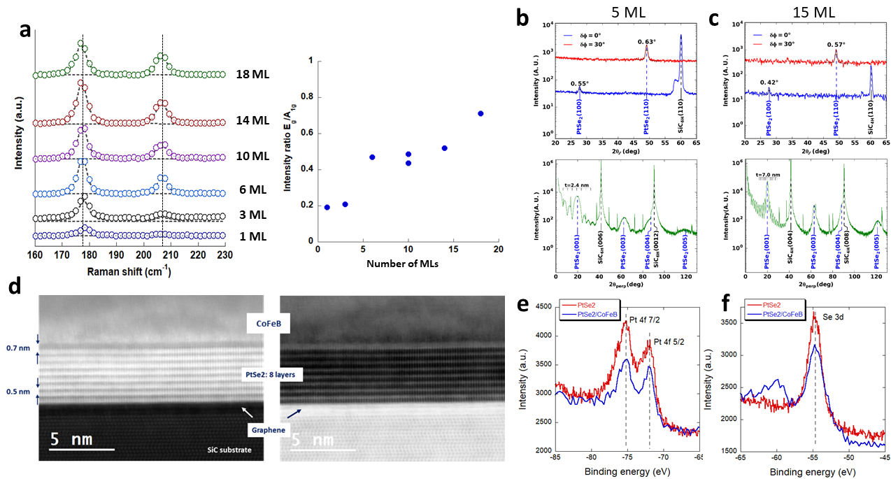
Next, in order to perform THz spintronic emission, we deposit 3 nm of amorphous CoFeB on top of PtSe2 covered by 4 nm of aluminum that transforms into AlOx to protect the ferromagnetic layer against oxidation. We use soft sputtering conditions for CoFeB deposition not to damage the PtSe2 surface. We set the argon pressure to 1.2510-2 mbar and the deposition rates are 0.319 Å/s for CoFeB and 0.265 Å/s for Al respectively. Moreover, the MBE evaporation chamber being connected to the magnetron sputtering reactor, all PtSe2 films are transferred in-situ under UHV conditions fully preserving the PtSe2 surface from contamination. In Fig. 2, we used a full set of characterization tools to study the impact of CoFeB deposition on PtSe2 properties. In Fig. 2a, all the Raman spectra for 1-18 ML of PtSe2 exhibit the two same Eg and A1g vibration modes demonstrating that the TMD film retains its crystal integrity after CoFeB deposition. For 10 ML of PtSe2, Eg and A1g peaks fall exactly at the same positions with and without CoFeB. We observe an increase of the Eg/A1g intensity ratio when increasing the thickness as already observed for pristine PtSe2 [19]. This result is confirmed by in-plane and out-of-plane x-ray diffraction as shown in Fig. 2b and 2c for 5 ML and 15 ML of PtSe2, respectively. First, the radial scans along the reciprocal directions at 0° and 30° of the substrate SiC(hh0) directions show the diffraction peaks of the substrate and PtSe2. The anisotropic character indicates that the layers are crystallographically well oriented in epitaxy with respect to the substrate. From the Bragg peak positions, we obtain the in-plane and out-of-plane lattice parameters: a=3.709 Å (resp. a=3.713 Å) and c=5.18 Å (resp. c=5.14 Å) for 5 ML (resp. 15 ML). They perfectly match the values obtained on 6 ML of PtSe2 without CoFeB. Moreover, the FWHM of in-plane (100) and (110) Bragg peaks (0.55°, 0.63° for 5 ML and 0.42°, 0.57° for 15 ML) are comparable to that of PtSe2 without CoFeB and confirms the large grain size. In addition, from the diffraction fringes around (001) Bragg peaks, we can conclude that the CoFeB/PtSe2 interface is flat at the atomic scale and deduce the film thickness to be 2.4 nm (2.5 nm expected) for 5 ML and 7.0 nm (expected 7.5 nm) for 15 ML.
These results confirm that PtSe2 films are not affected by the deposition of CoFeB. The interface atomic structure and chemical composition are further investigated by scanning transmission electron microscopy (STEM) in the high angular annular dark field (HAADF) mode and in situ x-ray photoemission spectroscopy (XPS) respectively. Fig. 2d shows in the dark and bright field modes 8 ML of PtSe2 epitaxially grown on Gr/SiC and covered by CoFeB. We clearly distinguish an atomically sharp interface with a 0.7 nm gap between the PtSe2 and CoFeB. In Fig. 2e and 2f, XPS spectra of Pt 4f and Se 3d core levels are recorded on 3 ML of PtSe2 before and after deposition of 1 nm of CoFeB. For both elements, the spectra superimpose before and after CoFeB deposition while the signal decrease after CoFeB deposition is due to the partial absorption of photoelectrons by the metallic film. To summarize, we can conclude from TEM and XPS analysis that the PtSe2 surface is preserved after CoFeB deposition.
II.2 THz spintronic emission
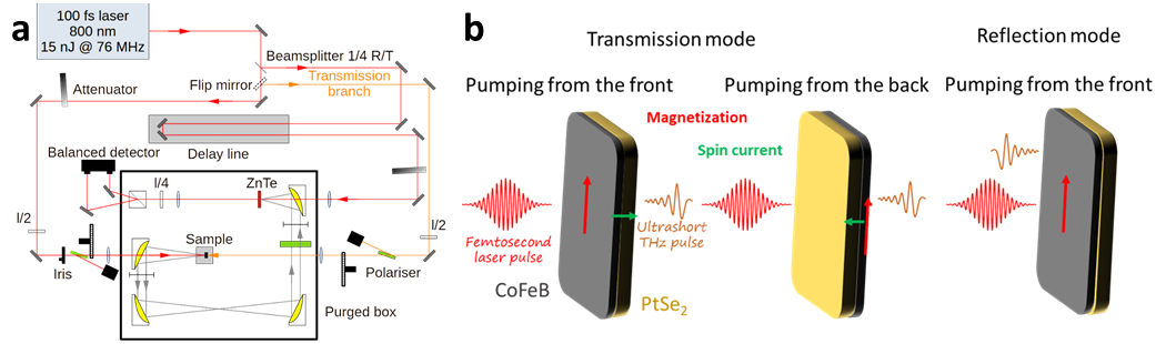
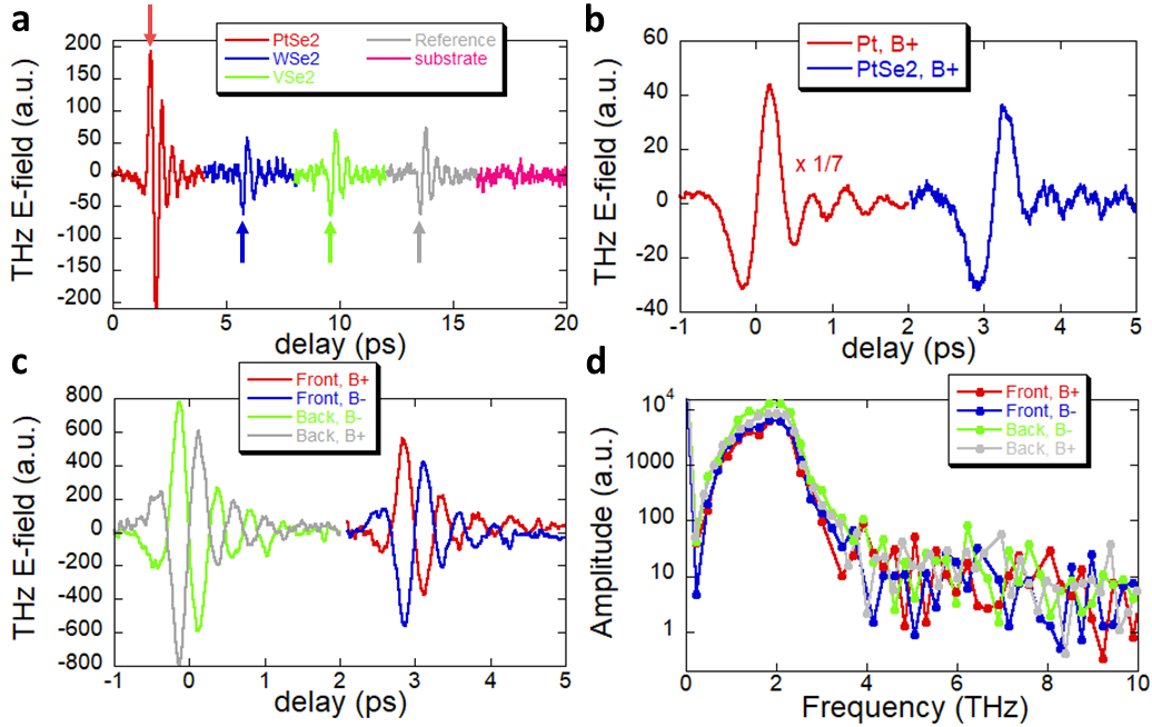
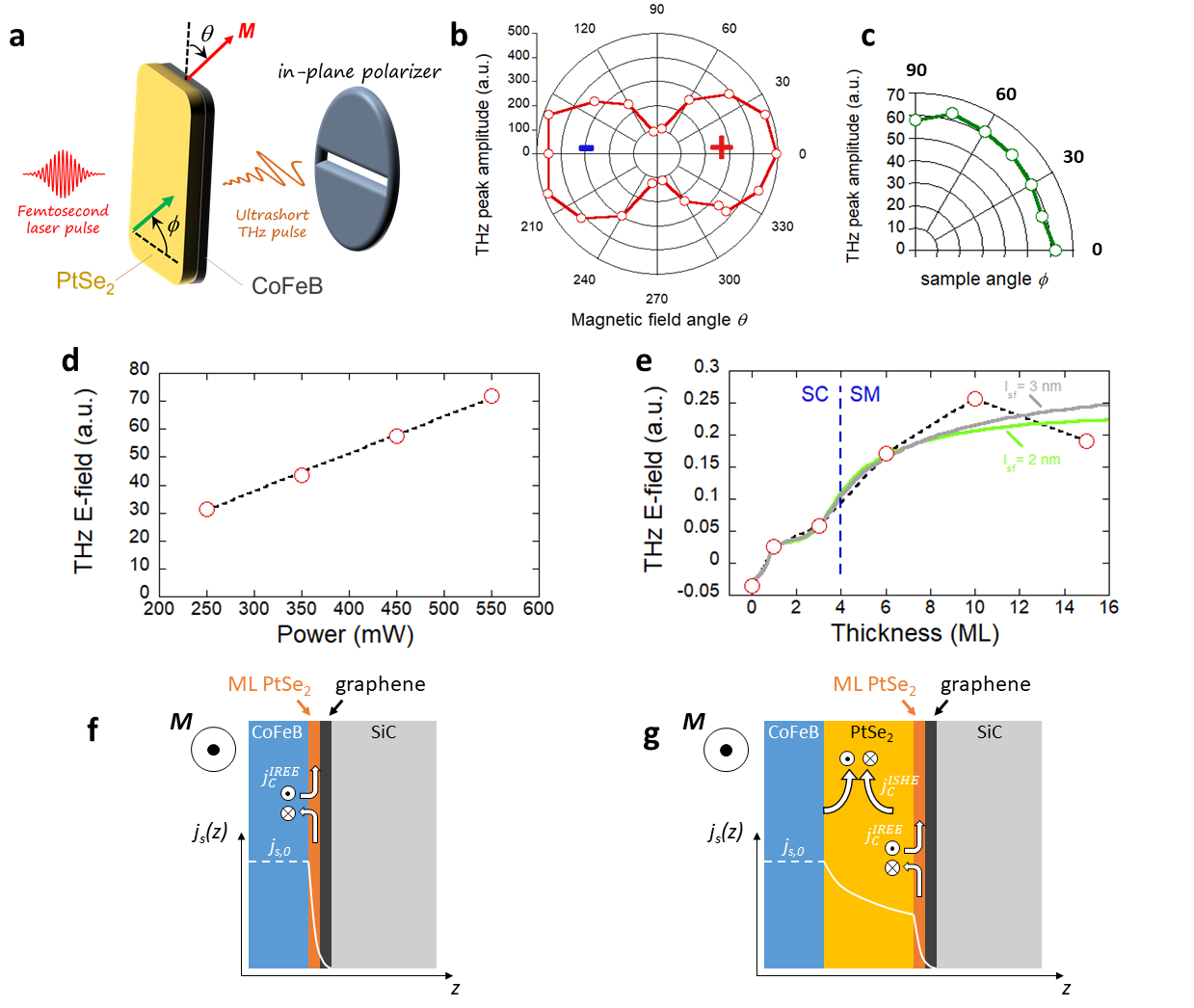
Measurements of the emitted THz waves from CoFeB/TMD samples are performed using THz emission time domain spectroscopy (TDS) as depicted in Fig. 3a. The sample is placed in a magnetic mount to apply an in-plane magnetic field of approximately 20 mT, with independent rotation of the sample and magnetic field. It is excited by a Ti:Sapphire oscillator (Coherent MIRA, 15-100 fs pulse length and horizontal polarization) at a wavelength of 800 nm in the near infrared (NIR) range. The average power exciting the sample is about 300 mW (after modulation by a chopper), adjustable by a half-wave plate followed by a polarizer. The emitted radiation is collected by a system of parabolic mirrors and the residual NIR pump is filtered by a Teflon plate. The last parabolic mirror with a hole in the center superimposes the emitted THz and the probe NIR pulse and focuses the THz beam on a ZnTe crystal for electro-optic detection with sensitivity set to horizontal component of the THz electric field (E-field). The ultrashort femtosecond laser pulse excites spin polarized electron-hole pairs in the ferromagnet (CoFeB) creating a net spin accumulation that generates a spin current into the non-magnetic layer (here the TMD) to be converted into a transverse charge current by ultrafast SCC. This results in an emitted electromagnetic pulse with frequencies in the THz range. As shown in Fig. 3b, we use both transmission (from the front and back sides) and reflection modes, which are used to show the spintronic origins of the THz emission. In Fig. 4a, we first compare spintronic THz emission from different samples: Gr/SiC bare substrate, CoFeB/Gr/SiC reference sample, CoFeB/VSe2, CoFeB/WSe2 and CoFeB/PtSe2. VSe2, WSe2 and PtSe2 are all 10 ML-thick. The epitaxial growth of VSe2 and WSe2 on graphene are detailed in [33] and [46], respectively. First, we clearly see that only CoFeB/PtSe2 gives an enhanced THz signal with respect to the reference sample. Moreover, the Gr/SiC substrate adds no background signal. Next, CoFeB/VSe2, CoFeB/WSe2 and the reference sample exhibit the same THz emitted signal in sign and amplitude. We thus conclude that the origin of SCC is the same in all three samples. The common feature between the three samples being the AlOx/CoFeB interface, we believe that the THz signal comes from the SCC at this interface through the inverse Rashba-Edelstein mechanism and/or from the self-emission of CoFeB due to unbalanced spin-flips at both interfaces. It also demonstrates that SCC in Gr/SiC, VSe2 and WSe2 is negligible. This can be justified by the low spin-orbit coupling of Gr/SiC and 1T-VSe2 whereas spin-valley locking favors out-of-plane spin polarization in 2H-WSe2 which partially prevents SCC when in-plane spins are injected. By looking at the first E-field maximum of each sample (indicated by arrows in Fig. 4a), we notice that it is opposite for PtSe2 pointing out another SCC mechanism taking place in PtSe2, opposite to the Rashba-Edelstein effect at the AlOx/CoFeB interface. In the following, we focus on THz spintronic emission from PtSe2. In Fig. 4b, we first compare the THz signals for pure Pt (5 nm) and PtSe2 (10 ML, 5 nm) with the magnetic field applied in the same direction (B+). The SCC in Pt and PtSe2 have the same sign and the magnitude is 7 times higher in Pt. Then, to verify the magnetic character of THz emission, we apply the magnetic field in two opposite directions (B+ and B-) and record the THz E-field in transmission mode by optically pumping the sample from the front and the back sides as shown in Fig. 4c. The opposite signs for B+ and B- and between front and back side pumping indicate the magnetic nature of the emission due to SCC in PtSe2. The overall signal being less when pumping from the front side, it proves that SiC partially absorbs THz waves. Finally, in Fig. 4d, we plot the Fourier transform of the 4 spectra shown in Fig. 4c and find the same broad band emission in the 0-4 THz range which is comparable to other THz spintronic emitters [47]. In order to study the influence of the ferromagnetic layer and deposition technique on THz emission, we performed the same measurements using 3 nm of cobalt deposited in situ on 10 ML of PtSe2 by electron beam evaporation (see Supp. Info.). We find very similar results showing that the ferromagnetic layer and deposition method have almost no influence on THz emission from PtSe2.
We then study the magnetic field angle () dependence in the geometry shown in Fig. 5a where a horizontal linear polarizer is introduced between the sample and the detector. Along a full 0°-360° rotation as shown in Fig. 5b, we obtain a typical cos() emission pattern with a phase reversal for opposite magnetic field directions (B+ at 0° and B- at 180°) which is a clear experimental evidence of SCC process in PtSe2. No sizeable asymmetry in the emission lobes is observed meaning that non-magnetic contributions to the THz signal are negligible in this material. Regarding the sample angle () dependence in Fig. 5c, we observe an isotropic signal with respect to the azimuthal crystalline orientation as expected for SCC like ISHE or IREE [48]. Moreover, the linear dependence of the THz signal (EB++EB-)/2 on the laser pump power in Fig. 5d is another experimental evidence of SCC in PtSe2.
II.3 SCC mechanism in PtSe2
In order to study the origin of SCC in PtSe2, we performed thickness dependent measurements as shown in Fig. 5e. For this, we pumped the magnetic layer from the backside and measured the THz signal in transmission mode. We took into account the absorption of the laser and THz waves by PtSe2 to normalize the signal (see Supp. Info.). The curve exhibits a two-step behavior that we interpret as IREE for thin PtSe2 coverage (first step) and ISHE for thicker PtSe2 (second step). Indeed, the second step appears at the semiconductor (SC) to semimetallic (SM) transition of PtSe2 as given by electrical van der Pauw measurements (see Supp. Info.). This is illustrated in Fig. 5f and 5g respectively where we assume that IREE takes place in the PtSe2 monolayer in contact with graphene and ISHE in the semi metallic bulk PtSe2. Based on these assumptions, we use a simple spin diffusion model to fit the experimental data. First, we assume that the spin current generated by optical excitation in CoFeB is completely absorbed in PtSe2 (spin sink model). We denote , , , and as the PtSe2 thickness, spin diffusion length in PtSe2, the spin current at the CoFeB/PtSe2 interface, the spin Hall angle of PtSe2 and effective spin Hall angle at the PtSe2/Gr interface, respectively. We use the following equations:
| (1) |
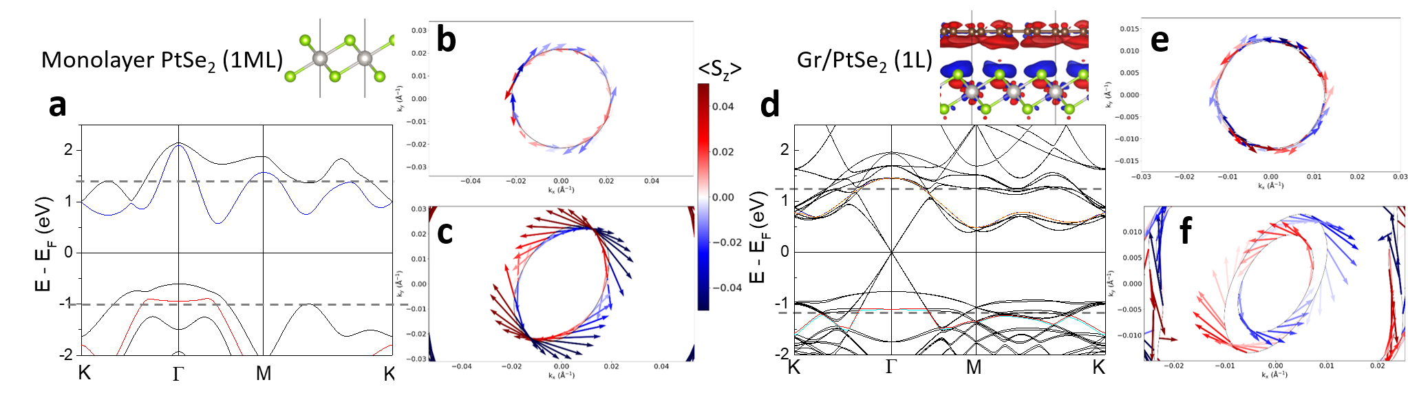
to describe the spin current at a depth from the CoFeB/PtSe2 interface and the layer-integrated spin current in PtSe2 . The profile of is depicted in Fig. 5f and 5g. The total charge current generated by IREE and ISHE can be written as: where is a step function and (resp. ) the PtSe2 thickness for which IREE (resp. ISHE) sets in. The Rashba-Edelstein length is then defined as: and we assume to be independent of . The best fit to the experimental data gives the following parameters: =0.35 nm; =1.7 nm; between 2 nm (green fitting curve in Fig. 5e) and 3 nm (grey fitting curve in Fig. 5e) and 2. is comparable to 1 ML of PtSe2 (0.27 nm) in agreement with IREE and corresponds to 3-4 ML of PtSe2 at the transition from semiconductor to semimetal in good agreement with ISHE. We find a short spin diffusion length between 2 nm (4 ML) and 3 nm (6 ML). The equivalent platinum thickness (corresponding to the Pt amount in 2 nm and 3 nm of PtSe2) is between 0.65 nm and 0.975 nm demonstrating that the spin flip rate with flow along the normal to the film plane is larger in PtSe2 than in Pt. This finding raises the question of spin diffusion with flow along the normal in lamellar systems. In particular, the role of van der Waals gaps needs to be taken into account. The short spin diffusion length could be explained if vdW gaps act as effective tunnel barriers in spin transport: during the tunnelling time between two PtSe2 layers, in-plane spin flips occur within individual PtSe2 layers limiting the vertical spin transport. This would deserve further investigation and the development of a more general theory which is out of the scope of the present work. Finally, we find that IREE and ISHE have the same sign and IREE is twice more efficient than ISHE. To support our conclusions and understand the mechanisms responsible for the THz spintronic emission, we have performed first principles calculations based on the projector-augmented wave (PAW) method [49] as implemented in the VASP package [50, 51, 52] using the generalized gradient approximation [53] and including spin-orbit coupling. The PtSe2/Gr heterostructure was constructed by matching 22 supercell of 1T-PtSe2 with 33 supercell of graphene on top so that to minimize the lattice mismatch to less than 1.5 %. A sufficient vacuum layer of 20 Å thickness was added to the heterostructure. The atomic coordinates were relaxed until the forces became smaller than 1 meV/Å. A kinetic energy cutoff of 550 eV has been used for the plane-wave basis set and a -centered 15151 k-mesh was used to sample the first Brillouin zone. To describe correctly the interaction across the interface, van der Waals forces were used with Grimme type dispersion-corrected density functional theory-D2 [54]. The two-dimensional spin textures were calculated for a 1010 -centered 2D k-mesh and the PyProcar package [55] was used to plot them. In Fig. 6a and 6d, we compare the calculated band structures for a freestanding PtSe2 and that of monolayer-PtSe2/Gr heterostructure. The relaxed interlayer distance between PtSe2 and Gr is found to be 3.29 Å which induces charge transfer across the interface depicted by the charge clouds in the inset of Fig. 6d. We estimate a charge transfer of about 0.04 transferred from the graphene to the PtSe2; a relatively small value that is consistent with the weak vdW interaction type. This is also reflected through the preserved band structure features of pristine graphene and PtSe2 in the heterostructure which is consistent with previous theoretical reports [56]. To assess the potential Rashba effect at PtSe2/Gr interface, the calculated spin textures for monolayer PtSe2 and PtSe2/Gr heterostructure are compared. Two representative bands are chosen: one in the conduction band (CB) and the other in the valence (VB) that are highlighted in blue and red in Fig. 6a, respectively. The corresponding two-dimensional spin textures displayed for the CB (VB) in Fig. 6b and 6c, show two contours with opposite spin helicities, however, they are degenerate with no splitting. This is implicit since there is no source of inversion symmetry breaking in a freestanding PtSe2 monolayer. In this respect, the spin textures observed in Refs.[18, 19] can only be explained by the presence of an interface electric field. Interfacing PtSe2 monolayer with graphene breaks the symmetry due to the interfacial dipole and thus induces a Rashba splitting of those bands as can be seen from the spin textures in Fig. 6e and 6f. Indeed, the band splitting is found to be larger for the VB with an estimated Rashba parameter meV.Å and can be explained by its orbital character which is mainly contributed by the p-orbitals of Se whereas the CB is dominated by Pt d-orbitals. Despite the fact that Pt has larger spin-orbit strength, the Se atoms are positioned at the interface which makes their bands more sensitive to the interfacial dipole effect. Although often neglected in the transition metal systems owing to the reduced hole velocity in the VB, the first step in THz emission (Fig. 6e) most probably originates from IREE in this valence band where spin polarized hot holes are injected from CoFeB. However, it is difficult to estimate the fraction of hot holes reaching this band since the position of the Fermi level altered by CoFeB deposition is unknown. ISHE in multilayers PtSe2, corresponding to the second step in THz emission (Fig. 6e), can be of extrinsic or intrinsic origin and further investigation would be required to identify its exact mechanism. Nevertheless, as shown in the Supp. Info., we already observe avoided band crossings in the VB of 3 ML PtSe2 that are supposed to contribute to intrinsic ISHE.
III Conclusion
In conclusion, we have realised large area and high quality 2D PtSe2 on graphene by molecular beam epitaxy, on which in-situ grown CoFeB is sputtered to study THz SCC phenomena. By performing a careful and extensive characterization of PtSe2 layers before and after CoFeB deposition, we find that the 2D material retains its structural and chemical properties. For SCC, we performed spintronic THz emission spectroscopy and find efficient THz emission from PtSe2, whereas VSe2 and WSe2 give negligible signals owing to low SOC and 1H crystal symmetry, respectively. From the PtSe2 heterostructures, we clearly demonstrate the magnetic origin of the THz signal and unveil the physical origin of the SCC through a PtSe2 thickness dependence study. The emitted THz electric field as a function of the number of PtSe2 monolayers exhibits a clear two-step behaviour, which reflects the transition from the IREE in semiconducting thin PtSe2 (3 ML) to ISHE in thicker semimetallic PtSe2 (3 ML). We also deduce the vertical spin diffusion length in PtSe2 to be 2-3 nm and find that IREE is twice as efficient compared to ISHE for SCC. Our conclusions are supported by first principles calculations showing the existence of Rashba SOC at the PtSe2/Gr interface. The unique band structure flexibility of PtSe2 makes it an ideal candidate as a THz spintronic 2D material and to further explore the underlying mechanisms and engineering of the SCC for THz emission.
IV Experimental Section
Raman spectroscopy
For Raman measurements, we used a Renishaw INVIA 1 spectrometer with a green laser (532 nm) and a 1800 gr/mm grating. The microscope objective magnification was 100 and the numerical aperture 0.9. The laser power was 150 W/m2. All the spectra correspond to the average of at least three spectra recorded at different locations on the samples.
X-ray diffraction
The grazing incidence X-ray diffraction (GIXD) was done with a SmartLab Rigaku diffractometer equipped with a copper rotating anode beam tube (Kα=1.54 Å) operating at 45 kV and 200 mA. Parallel in-plane collimators of 0.5° of resolution were used both on the source and detector sides. The out-of-plane XRD measurements were performed using a Panalytical Empyrean diffractometer operated at 35 kV and 50 mA, with a cobalt source, (Kα= 1.79 Å). A PIXcel-3D detector allowed a resolution of 0.02° per pixel, in combination with a divergence slit of 0.125°. Both diffractometers are equipped with multilayer mirror on the incident beam and Kβ filter on the diffracted beam.
Transmission electron microscopy
Scanning transmission electron microscopy (STEM) measurements
were performed using a Cs-corrected FEI
Themis at 200 kV. HAADF-STEM (high-angle annular
dark field) images were acquired using a convergence angle
of 20 mrad and collecting electrons scattered at angles
higher than 60 mrad. STEM specimens were prepared by
the focused ion beam (FIB) lift-out technique using a Zeiss
Crossbeam 550. The sample was coated with protective
carbon and platinum layers prior to the FIB cut.
X-ray photoemission spectroscopy
XPS was performed in situ using a Staib Instruments spectrometer. We used an aluminum anode with emission operating at 300 W. The signal was optimized on the Se LMM Auger spectra at a binding energy of 184 eV. The C1s line was used to set the binding energy scale.
V Acknowledgements
The authors acknowledge the support from the European Union’s Horizon 2020 research and innovation Programme under grant agreement No 881603 (Graphene Flagship), No 829061 (FET-OPEN NANOPOLY) and No 964735 (FET-OPEN EXTREME-IR). The French National Research Agency (ANR) is acknowledged for its support through the ANR-18-CE24-0007 MAGICVALLEY and ESR/EQUIPEX+ ANR-21-ESRE-0025 2D-MAG projects. The LANEF framework (No. ANR-10-LABX-0051) is acknowledged for its support with mutualized infrastructure.
References
- [1] Novoselov, K., Geim, A., Morozov, S., Jiang, D., Zhang, Y., Dubonos, S., Grigorieva, I. & A. A. Firsov Electric Field Effect in Atomically Thin Carbon Films. Science. 306, 666-669 (2004).
- [2] Novoselov, K., Geim, A., Morozov, S., Jiang, D., Katsnelson, M., Grigorieva, I., Dubonos, S. & Firsov, A. Two-dimensional gas of massless Dirac fermions in graphene. Nature. 438, 197-200 (2005).
- [3] Cao, Y., Fatemi, V., Fang, S., Watanabe, K., Taniguchi, T., Kaxiras, E. & Jarillo-Herrero, P. Unconventional superconductivity in magic-angle graphene superlattices. Nature. 556, 43-50 (2018).
- [4] Mak, K., Lee, C., Hone, J., Shan, J. & Heinz, T. Atomically Thin MoS2: A New Direct-Gap Semiconductor. Phys. Rev. Lett.. 105, 136805 (2010).
- [5] Cadiz, F., Courtade, E., Robert, C., Wang, G., Shen, Y., Cai, H., Taniguchi, T., Watanabe, K., Carrere, H., Lagarde, D., Manca, M., Amand, T., Renucci, P., Tongay, S., Marie, X. & Urbaszek, B. Excitonic Linewidth Approaching the Homogeneous Limit in MoS2-Based van der Waals Heterostructures. Phys. Rev. X. 7, 021026 (2017).
- [6] Xiao, D., Liu, G., Feng, W., Xu, X. & Yao, W. Coupled Spin and Valley Physics in Monolayers of MoS2 and Other Group-VI Dichalcogenides. Phys. Rev. Lett.. 108, 196802 (2012).
- [7] Sallen, G., Bouet, L., Marie, X., Wang, G., Zhu, C., Han, W., Lu, Y., Tan, P., Amand, T., Liu, B. & Urbaszek, B. Robust optical emission polarization in MoS2 monolayers through selective valley excitation. Phys. Rev. B. 86, 081301 (2012).
- [8] Mak, K., McGill, K., Park, J. & P. L. McEuen The valley Hall effect in MoS2 transistors. Science. 344, 1489-1492 (2014).
- [9] Dau, M., Vergnaud, C., Marty, A., Beigné, C., Gambarelli, S., Maurel, V., Journot, T., Hyot, B., Guillet, T., Grévin, B., Okuno, H. & Jamet, M. The valley Nernst effect in WSe2. Nature Communications. 10, 5796 (2019).
- [10] Benítez, L., Sierra, J., Savero Torres, W., Arrighi, A., Bonell, F., Costache, M. & Valenzuela, S. Strongly anisotropic spin relaxation in graphene–transition metal dichalcogenide heterostructures at room temperature. Nature Physics. 14, 303-308 (2018).
- [11] Guimarães, M., Stiehl, G., MacNeill, D., Reynolds, N. & Ralph, D. Spin–Orbit Torques in NbSe2/Permalloy Bilayers. Nano Letters. 18, 1311-1316 (2018).
- [12] Zhao, Y., Qiao, J., Yu, Z., Yu, P., Xu, K., Lau, S., Zhou, W., Liu, Z., Wang, X., Ji, W. & Chai, Y. High-Electron-Mobility and Air-Stable 2D Layered PtSe2 FETs. Advanced Materials. 29, 1604230 (2017).
- [13] Bonell, F., Marty, A., Vergnaud, C., Consonni, V., Okuno, H., Ouerghi, A., Boukari, H. & Jamet, M. High carrier mobility in single-crystal PtSe2 grown by molecular beam epitaxy on ZnO(0001). 2D Materials. 9, 015015 (2021).
- [14] Cao, B., Ye, Z., Yang, L., Gou, L. & Wang, Z. Recent progress in Van der Waals 2D PtSe2. Nanotechnology. 32, 412001 (2021).
- [15] Avsar, A., Cheon, C., Pizzochero, M., Tripathi, M., Ciarrocchi, A., Yazyev, O. & Kis, A. Probing magnetism in atomically thin semiconducting PtSe2. Nature Communications. 11, 4806 (2020).
- [16] Sant, R., Gay, M., Marty, A., Lisi, S., Harrabi, R., Vergnaud, C., Dau, M., Weng, X., Coraux, J., Gauthier, N., Renault, O., Renaud, G. & Jamet, M. Synthesis of epitaxial monolayer Janus SPtSe. Npj 2D Materials And Applications. 4, 41 (2020).
- [17] Villaos, R., Crisostomo, C., Huang, Z., Huang, S., Padama, A., Albao, M., Lin, H. & Chuang, F. Thickness dependent electronic properties of Pt dichalcogenides. Npj 2D Materials And Applications. 3, 2 (2019).
- [18] Yao, W., Wang, E., Huang, H., Deng, K., Yan, M., Zhang, K., Miyamoto, K., Okuda, T., Li, L., Wang, Y., Gao, H., Liu, C., Duan, W. & Zhou, S. Direct observation of spin-layer locking by local Rashba effect in monolayer semiconducting PtSe2 film. Nature Communications. 8, 14216 (2016).
- [19] Yan, M., Wang, E., Zhou, X., Zhang, G., Zhang, H., Zhang, K., Yao, W., Lu, N., Yang, S., Wu, S., Yoshikawa, T., Miyamoto, K., Okuda, T., Wu, Y., Yu, P., Duan, W. & Zhou, S. High quality atomically thin PtSe2 films grown by molecular beam epitaxy. 2D Materials. 4, 045015 (2017).
- [20] Bangar, H., Kumar, A., Chowdhury, N., Mudgal, R., Gupta, P., Yadav, R., Das, S. & Muduli, P. Large Spin-To-Charge Conversion at the Two-Dimensional Interface of Transition-Metal Dichalcogenides and Permalloy. ACS Applied Materials & Interfaces. 14, 41598-41604 (2022).
- [21] Seifert, T., Jaiswal, S., Martens, U., Hannegan, J., Braun, L., Maldonado, P., Freimuth, F., Kronenberg, A., Henrizi, J., Radu, I., Beaurepaire, E., Mokrousov, Y., Oppeneer, P., Jourdan, M., Jakob, G., Turchinovich, D., Hayden, L., Wolf, M., Münzenberg, M., Kläui, M. & Kampfrath, T. Efficient metallic spintronic emitters of ultrabroadband terahertz radiation. Nature Photonics. 10, 483-488 (2016).
- [22] Rongione, E., Baringthon, L., She, D., Patriarche, G., Lebrun, R., Lemaître, A., Morassi, M., Reyren, N., Mičica, M., Mangeney, J., Tignon, J., Bertran, F., Dhillon, S., Le Fèvre, P., Jaffrès, H. & George, J. Spin-Momentum Locking and Ultrafast Spin-Charge Conversion in Ultrathin Epitaxial Bi1-xSbx Topological Insulator. Advanced Science. n/a, 2301124.
- [23] Hawecker, J., Dang, T., Rongione, E., Boust, J., Collin, S., George, J., Drouhin, H., Laplace, Y., Grasset, R., Dong, J., Mangeney, J., Tignon, J., Jaffrès, H., Perfetti, L. & Dhillon, S. Spin Injection Efficiency at Metallic Interfaces Probed by THz Emission Spectroscopy. Advanced Optical Materials. 9, 2100412 (2021).
- [24] Dang, T., Hawecker, J., Rongione, E., Baez Flores, G., To, D., Rojas-Sanchez, J., Nong, H., Mangeney, J., Tignon, J., Godel, F., Collin, S., Seneor, P., Bibes, M., Fert, A., Anane, M., George, J., Vila, L., Cosset-Cheneau, M., Dolfi, D., Lebrun, R., Bortolotti, P., Belashchenko, K., Dhillon, S. & Jaffrès, H. Ultrafast spin-currents and charge conversion at 3d-5d interfaces probed by time-domain terahertz spectroscopy. Applied Physics Reviews. 7, 041409 (2020).
- [25] Cheng, L., Li, Z., Zhao, D. & Chia, E. Studying spin–charge conversion using terahertz pulses. APL Materials. 9, 070902 (2021).
- [26] Cheng, L., Wang, X., Yang, W., Chai, J., Yang, M., Chen, M., Wu, Y., Chen, X., Chi, D., Goh, K., Zhu, J., Sun, H., Wang, S., Song, J., Battiato, M., Yang, H. & Chia, E. Far out-of-equilibrium spin populations trigger giant spin injection into atomically thin MoS2. Nature Physics. 15, 347-351 (2019).
- [27] Nádvorník, L., Gueckstock, O., Braun, L., Niu, C., Gräfe, J., Richter, G., Schütz, G., Takagi, H., Zeer, M., Seifert, T., Kubaščík, P., Pandeya, A., Anane, A., Yang, H., Bedoya-Pinto, A., Parkin, S., Wolf, M., Mokrousov, Y., Nakamura, H. & Kampfrath, T. Terahertz Spin-to-Charge Current Conversion in Stacks of Ferromagnets and the Transition-Metal Dichalcogenide NbSe2. Advanced Materials Interfaces. 9, 2201675 (2022).
- [28] Khusyainov, D., Guskov, A., Ovcharenko, S., Tiercelin, N., Preobrazhensky, V., Buryakov, A., Sigov, A. & Mishina, E. Increasing the Efficiency of a Spintronic THz Emitter Based on WSe2/FeCo. Materials. 14 (2021).
- [29] Cong, K., Vetter, E., Yan, L., Li, Y., Zhang, Q., Xiong, Y., Qu, H., Schaller, R., Hoffmann, A., Kemper, A., Yao, Y., Wang, J., You, W., Wen, H., Zhang, W. & Sun, D. Coherent control of asymmetric spintronic terahertz emission from two-dimensional hybrid metal halides. Nature Communications. 12, 5744 (2021).
- [30] Dau, M., Gay, M., Di Felice, D., Vergnaud, C., Marty, A., Beigné, C., Renaud, G., Renault, O., Mallet, P., Le Quang, T., Veuillen, J., Huder, L., Renard, V., Chapelier, C., Zamborlini, G., Jugovac, M., Feyer, V., Dappe, Y., Pochet, P. & Jamet, M. Beyond van der Waals Interaction: The Case of MoSe2 Epitaxially Grown on Few-Layer Graphene. ACS Nano. 12, 2319-2331 (2018).
- [31] Dau, M., Vergnaud, C., Gay, M., Alvarez, C., Marty, A., Beigné, C., Jalabert, D., Jacquot, J., Renault, O., Okuno, H. & Jamet, M. van der Waals epitaxy of Mn-doped MoSe2 on mica. APL Materials. 7, 051111 (2019).
- [32] Vergnaud, C., Dau, M., Grévin, B., Licitra, C., Marty, A., Okuno, H. & Jamet, M. New approach for the molecular beam epitaxy growth of scalable WSe2 monolayers. Nanotechnology. 31, 255602 (2020).
- [33] Vélez-Fort, E., Hallal, A., Sant, R., Guillet, T., Abdukayumov, K., Marty, A., Vergnaud, C., Jacquot, J., Jalabert, D., Fujii, J., Vobornik, I., Rault, J., Brookes, N., Longo, D., Ohresser, P., Ouerghi, A., Veuillen, J., Mallet, P., Boukari, H., Okuno, H., Chshiev, M., Bonell, F. & Jamet, M. Ferromagnetism and Rashba Spin–Orbit Coupling in the Two-Dimensional (V,Pt)Se2 Alloy. ACS Applied Electronic Materials. 4, 259-268 (2022).
- [34] Kumar, B., Baraket, M., Paillet, M., Huntzinger, J., Tiberj, A., Jansen, A., Vila, L., Cubuku, M., Vergnaud, C., Jamet, M., Lapertot, G., Rouchon, D., Zahab, A., Sauvajol, J., Dubois, L., Lefloch, F. & Duclairoir, F. Growth protocols and characterization of epitaxial graphene on SiC elaborated in a graphite enclosure. Physica E: Low-dimensional Systems And Nanostructures. 75 pp. 7-14 (2016).
- [35] Pallecchi, E., Lafont, F., Cavaliere, V., Schopfer, F., Mailly, D., Poirier, W. & Ouerghi, A. High Electron Mobility in Epitaxial Graphene on 4H-SiC(0001) via post-growth annealing under hydrogen. Scientific Reports. 4, 4558 (2014).
- [36] El Sachat, A., Xiao, P., Donadio, D., Bonell, F., Sledzinska, M., Marty, A., Vergnaud, C., Boukari, H., Jamet, M., Arregui, G., Chen, Z., Alzina, F., Sotomayor Torres, C. & Chavez-Angel, E. Effect of crystallinity and thickness on thermal transport in layered PtSe2. Npj 2D Materials And Applications. 6, 32 (2022).
- [37] Li, J., Kolekar, S., Ghorbani-Asl, M., Lehnert, T., Biskupek, J., Kaiser, U., Krasheninnikov, A. & Batzill, M. Layer-Dependent Band Gaps of Platinum Dichalcogenides. ACS Nano. 15, 13249-13259 (2021).
- [38] Zhang, L., Yang, T., Sahdan, M., Arramel, Xu, W., Xing, K., Feng, Y., Zhang, W., Wang, Z. & Wee, A. Precise Layer-Dependent Electronic Structure of MBE-Grown PtSe2. Advanced Electronic Materials. 7, 2100559 (2021).
- [39] Wu, X., Qiao, J., Liu, L., Shao, Y., Liu, Z., Li, L., Zhu, Z., Wang, C., Hu, Z., Ji, W., Wang, Y. & Gao, H. Shallowing interfacial carrier trap in transition metal dichalcogenide heterostructures with interlayer hybridization. Nano Research. 14, 1390-1396 (2021).
- [40] Hibino, H., Kageshima, H., Kotsugi, M., Maeda, F., Guo, F. & Watanabe, Y. Dependence of electronic properties of epitaxial few-layer graphene on the number of layers investigated by photoelectron emission microscopy. Phys. Rev. B. 79, 125437 (2009).
- [41] Liu, Y., Stradins, P. & Su-Huai Wei Van der Waals metal-semiconductor junction: Weak Fermi level pinning enables effective tuning of Schottky barrier. Science Advances. 2, e1600069 (2016).
- [42] Filleter, T., Emtsev, K., Seyller, T. & Bennewitz, R. Local work function measurements of epitaxial graphene. Applied Physics Letters. 93, 133117 (2008).
- [43] Quang, T., Cherkez, V., Nogajewski, K., Potemski, M., Dau, M., Jamet, M., Mallet, P. & Veuillen, J. Scanning tunneling spectroscopy of van der Waals graphene/semiconductor interfaces: absence of Fermi level pinning. 2D Materials. 4, 035019 (2017).
- [44] Dappe, Y., Almadori, Y., Dau, M., Vergnaud, C., Jamet, M., Paillet, C., Journot, T., Hyot, B., Pochet, P. & Grévin, B. Charge transfers and charged defects in WSe2/graphene-SiC interfaces. Nanotechnology. 31, 255709 (2020).
- [45] Furuseth, S., Selte, K. & Kjekshus, A. Redetermined Crystal Structures of NiTe2, PdTe2, PtS2, PtSe2, and PtTe2. Acta Chemica Scandinavica. 19, 735-741 (1965).
- [46] Dau, M., Vergnaud, C., Marty, A., Beigné, C., Gambarelli, S., Maurel, V., Journot, T., Hyot, B., Guillet, T., Grévin, B., Okuno, H. & Jamet, M. The valley Nernst effect in WSe2. Nature Communications. 10, 5796 (2019).
- [47] Wang, M., Zhang, Y., Guo, L., Lv, M., Wang, P. & Wang, X. Spintronics Based Terahertz Sources. Crystals. 12 (2022).
- [48] Rongione, E., Fragkos, S., Baringthon, L., Hawecker, J., Xenogiannopoulou, E., Tsipas, P., Song, C., Mičica, M., Mangeney, J., Tignon, J., Boulier, T., Reyren, N., Lebrun, R., George, J., Le Fèvre, P., Dhillon, S., Dimoulas, A. & Jaffrès, H. Ultrafast Spin-Charge Conversion at SnBi2Te4/Co Topological Insulator Interfaces Probed by Terahertz Emission Spectroscopy. Advanced Optical Materials. 10, 2102061 (2022).
- [49] Blöchl, P. Projector augmented-wave method. Phys. Rev. B. 50, 17953-17979 (1994).
- [50] Kresse, G. & Hafner, J. Ab initio molecular dynamics for liquid metals. Phys. Rev. B. 47, 558-561 (1993).
- [51] Kresse, G. & Furthmüller, J. Efficient iterative schemes for ab initio total-energy calculations using a plane-wave basis set. Phys. Rev. B. 54, 11169-11186 (1996).
- [52] Kresse, G. & Furthmüller, J. Efficiency of ab-initio total energy calculations for metals and semiconductors using a plane-wave basis set. Computational Materials Science. 6, 15-50 (1996).
- [53] Perdew, J., Burke, K. & Ernzerhof, M. Generalized Gradient Approximation Made Simple. Phys. Rev. Lett.. 77, 3865-3868 (1996).
- [54] Bučko, T., Hafner, J., Lebègue, S. & Ángyán, J. Improved Description of the Structure of Molecular and Layered Crystals: Ab Initio DFT Calculations with van der Waals Corrections. The Journal Of Physical Chemistry A. 114, 11814-11824 (2010).
- [55] Herath, U., Tavadze, P., He, X., Bousquet, E., Singh, S., Muñoz, F. & Romero, A. PyProcar: A Python library for electronic structure pre/post-processing. Computer Physics Communications. 251 pp. 107080 (2020).
- [56] Sattar, S. & Schwingenschlögl, U. Electronic Properties of Graphene–PtSe2 Contacts. ACS Applied Materials & Interfaces. 9, 15809-15813 (2017)