Brightness and purity of a room-temperature single-photon source in the blue-green range
Abstract
We discuss a promising solid-state system that emits single photons at room temperature in the blue-green range, making it an attractive candidate for quantum communications in free space and underwater. The active element is a core-shell ZnSe tapered nanowire embedding a single CdSe quantum dot grown by molecular beam epitaxy. A patterned substrate enables a comprehensive study of a single nanowire using various methods. Our source shows potential for achieving a total brightness of 0.17 photon per pulse and anti-bunching with within a restricted spectral window. Additionally, we analyze the impact of charged excitons on the value in different spectral ranges.
1 Univ. Grenoble-Alpes, CEA, Grenoble INP, IRIG, PHELIQS, NPSC, 38000 Grenoble, France
2 Univ. Grenoble-Alpes, CNRS, Inst. NEEL, 38042 Grenoble, France
* Correspondence: francis.granger@cea.fr, kuntheak.kheng@cea.fr
Quantum communication is a rapidly growing field with enormous potential for secure data transmission. One major challenge in this field is the development of single-photon sources (SPS) that can effectively generate on-demand single photons for use in quantum information systems. The main advantage of using solid-state systems such as quantum dots (QDs) is that they present a high purity of the emitted single-photons, making them ideal for use as flying qubits in quantum key distribution protocols [1]. In contrast to classical bits, flying qubits cannot be cloned, making it impossible for eavesdroppers to intercept the transmission secretly.
Many single-photon sources are based on III-V grown QDs and exhibit spectrally narrow lines in near infra-red when operating at cryogenic temperatures, with impressive performances in terms of brightness and purity [2, 3]. However, the need for cryogenic temperatures is still a major drawback for practically implementing these emitters in quantum information systems, despite efforts toward elevated temperatures [4, 5, 6]. Nitride semiconductors have shown room-temperature single-photon emission at different wavelengths [7, 8, 9]. CdSe QDs offer an alternative solution, as they are operational at 300K [10, 11]. They emit in the blue-green range, thus allowing for free-space long-distance communication in seawater and air [12]. This makes them an attractive alternative for real-world implementation of SPS in quantum information systems. Efficient light extraction from QDs is a critical issue towards high emission rates. A good way to achieve this is to embed a QD in a nanowire (NW) [13, 3, 14] which acts as a single-mode waveguide channeling the photons emitted by the QD. Furthermore, a tapered NW improves the control of the emission properties. The tapered shape adiabatically expands the guided mode and reduces the divergence angle, increasing the collection efficiency [15, 16, 3, 14].
We report here on a SPS based on a semiconductor QD-tapered NW, with purity , emitting in the blue-green range and operating at room temperature. Our study focuses on a unique QD-NW submitted to a whole range of characterizations, although other emitters on the same sample exhibit similar properties.
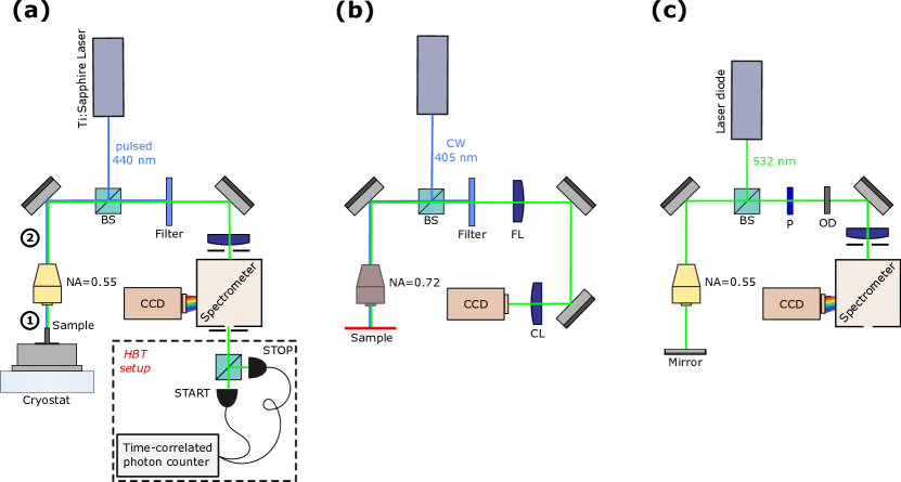
We have used molecular beam epitaxy (MBE) to grow, at 350°C on a GaAs (111)B substrate, the ZnSe core embedding a CdSe QD near its top (Fig. 1(a)). This was followed by the growth at 320°C of a tapered ZnSe shell. Growth conditions are detailed in Refs. [17] and [18]. The epiready substrate was patterned before growth by combining laser lithography with chemical etching, enabling the NW position to be marked and allowing several observations on the same NW by switching from one experimental setup to another.
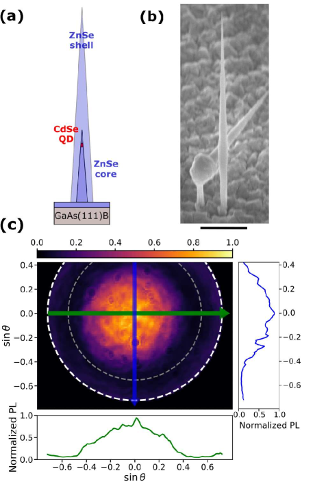
The vertical NW depicted in this article was selected from its far-field emission diagram recorded using Fourier imaging [19]. To this purpose, we use a high numerical aperture objective () along with a cw excitation laser at 405 nm. Then, we performed micro-photoluminescence measurements (µ-PL) as well as time-resolved photoluminescence (TRPL) in a second setup with non-resonant pulsed excitation from a titanium-sapphire laser frequency-doubled to 440 nm (repetition time ns, frequency MHz). Light is collected through a objective and sent to a spectrometer equipped with a 600 grooves/mm grating (input slit width 0.2 mm). In order to identify the involved transitions, complementary measurements were performed at cryogenic temperature using a 1800 grooves/mm grating and a slit width of 0.05 mm. A Hanbury Brown and Twiss (HBT) setup composed of two fast avalanche photodiodes (APD) allowed us to characterize the purity of the SPS through correlation measurements. Finally, the NW was observed under a Scanning Electron Microscope (SEM), as displayed in Fig. 1(b).
The 1 µm scale bar is of the same order as the diameter of the excitation laser spot. The vertical NW has a base diameter of 140 nm and a height of 5 µm. The far-field diagram in Fig. 1(c) shows that the photons emitted upward exhibit a Gaussian mode profile with divergence angle such that at half maximum, in agreement with previous studies on NWs with a small taper angle [15, 16]. Note that the upward emission of a CdSe QD without the thick tapered ZnSe shell is very weak due to the dielectric screening present in nanowires with small diameters [20]. The tapered shell ensures an adiabatic coupling between the guided mode and free space, leading to a collection efficiency within calculated to be close to unity. Measurements in Fig. 1(c) show that 85% of the collected light falls within . We note that light emitted towards the substrate is lost, leading to a theoretical maximum source efficiency close to 50%. Additionally, the microscope objective with shows a transmission of 90% at the wavelength of interest [21]. Thus, an ideal SPS made of a QD inserted in the present NW would provide a photon flux around 0.38 photon per pulse at the output of this objective.
The QD-NW room temperature µ-PL spectra are shown in Fig. 2 for values of the pulsed excitation power ranging from 0.2 to 6 µW. We observe two peaks at 582.5 nm (L1) and 586.5 nm (L2). It can be seen qualitatively that the L1 intensity grows linearly with , while L2 grows at a faster rate. At µW, the QD starts to saturate. Using the setup calibration explained in Supplement 1, the number of photons collected out of the microscope objective for L1 and L2 together yield to a promising value of 0.28 photon per pulse. This is discussed later on.
The onset of saturation around µW was confirmed by further measurements up to 20 µW. However, these measurements at high-power caused an evolution of the spectrum, as seen in the inset of Fig. 3(a) for µW. The L1 intensity decreased significantly and L2 to a lesser extent. After this evolution, L1 + L2 signals yield to 0.09 photon per pulse, a value which remained constant for weeks after this initial decrease.
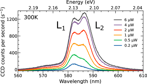
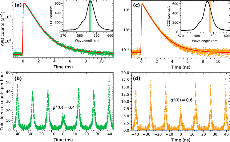
Figure 3 shows the TRPL signal of the QD-NW emission within a spectral window of nm (blue arrow labeled 1 in the inset). The red solid line in Fig. 3(a) is the convolution of the response function of the setup (a Gaussian with a FWHM of 60 ps [22]), and a sum of three exponential functions added to a constant baseline:
| (1) |
The main component is a decay with a short lifetime ns. There is also a weak, slow component, with ns and . The term , introduced to describe a population rise of the emitting state, was found to be hidden by the time-resolution of the APD [22].
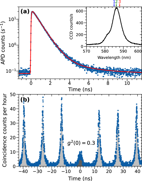
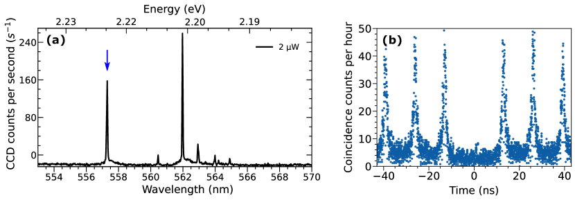
The purity of the SPS was determined using a HBT autocorrelation measurement. The coincidence histogram for the same conditions as in Fig. 3(a) and the same spectral window (1 nm centered on the blue arrow) is shown in Fig. 3(b). Under pulsed excitation, a series of correlation peaks appear, with equal spacing given by the laser repetition period . The peak widths agree with the lifetime . As , the purity is computed using the ratio of the central peak area to the lateral ones. At 585.0 nm, our system exhibits a second-order correlation at zero delays , below the threshold of 0.5 considered as a signature of single-photon emission.
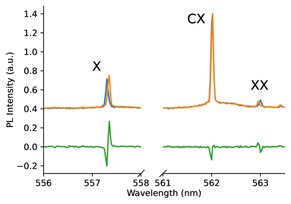
It is difficult to identify the nature of L1 and L2 from the spectra at room temperature, but this can be done by a comparison with the PL spectrum at 6K shown in Fig. 4(c). Sharp zero-phonon lines lie on top of broad acoustic-phonon sidebands. Polarization-resolved PL spectra (see Supplement 1) allow us to observe a fine structure splitting with opposite signs for two of those lines, therefore attributed to the neutral exciton X and biexciton XX. This agrees with the linear and quadratic behavior observed in Fig. 2. The most intense line in Fig. 4(c) shows no fine structure. Hence, it is attributed to a charged exciton CX. A similar spectral arrangement of the X, CX, and XX lines has been observed previously on similar samples [23]. The CX line was attributed to the positively charged exciton in Ref. [24], and the lines with energies smaller than XX were attributed to the charged biexciton CXX in Refs. [24, 25]. Finally, the small line at 560.8 nm in Fig. 4(c) was attributed to the negatively charged exciton X- in [20]. We note a large splitting of 5.66 nm (22.4 meV) between the X and XX lines.
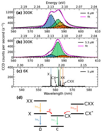
At room temperature, the zero-phonon lines are vanishingly small, and the spectra only show broad phonon sidebands. The spectra for µW in Fig. 2 and the inset of Fig.3(a) are fitted and displayed in Fig.4(a) and (b), respectively. They comprise four Voigt functions and a constant baseline. The position of each line is set to match the relative positions of the X, CX, XX, and CXX lines in Fig. 4(c). The X, CX, and XX linewidths are constrained to a common value, while CXX, composed of several lines, has a larger width. Assuming that the trapping of electron-hole pairs does not depend on the presence of charges in the QD, the amplitude of each line is set so that the ratios of intensities obey .
The fit in Fig. 4(b) results in a X, CX, and XX linewidth equal to 5.2 nm (19 meV), and 7.2 nm (26 meV) for CXX. The common biexciton/exciton intensity ratio is 0.45, illustrating that we are not fully at saturation at µW. Although X is dominant in Fig. 4 (a), the contribution of CX is sizable with . The lines X and CX together yield 0.17 photon per pulse.
The ratios in Fig. 4 (b) indicate that either the spectrum (after the intensity decrease) is further away from saturation, or that non-radiative processes reduce the X emission intensity. Additionally, the ratio shows that CX dominates X. In Fig. 4 (b), the X and CX lines together contribute for 0.06 photon per pulse. Figure 3(a) displays the decay at 585.0 nm, where the fit shows that the strongest contribution is due to the CX line, with a small overlap with CXX and X lines. The corresponding decay curve (Fig 3(a)) exhibits a dominant exponential decay with a sub-nanosecond lifetime ( ns), a value slightly larger than the lifetime reported in Ref. [18]. Moreover, the fast rise is in good agreement with an excitation power far from saturation.
We also investigated the impact of the spectral window position on the emitter’s purity. At 585.0 nm (blue arrow in the inset of Fig. 3(a)), the zero-delay correlation peak is . We measure close to L2 peak center (green arrow labeled as 2 in the inset) and on the red side of L2 (red arrow labeled as 3). See Supplement 1 for additional data. Each of these 1nm-broad portions of the spectrum yields to approximately 0.02 photon per pulse. We discuss below how higher values can be achieved. Shifting from spectral window 1 to 3, the overlap between CX and CXX increases, enhancing a correlation through the biexciton-exciton cascade in the charged QD. Coming back to spectral window 1, there is still some CX-CXX overlap at 585.0 nm but we cannot rule out the possibility of a cross radiative cascade resulting from a fast charge trapping forming the positively charged exciton , as illustrated in Fig. 4(d). We may expect to increase the purity even more () by blue-shifting the spectral window below 585 nm. This would make it possible to identify the role of the cross-cascade. However, the intensity diminishes drastically as we shift the spectral window to lower wavelengths. There is an unavoidable tradeoff between purity which requires a narrow spectral window, and brightness, where a broad spectral bandwidth with high intensity is needed.
In conclusion, we demonstrate a promising triggered SPS operational at room temperature, with large X-XX splitting of 5.66 nm (22.4 meV), enabling us to obtain a high single-photon purity with . We identify neutralizing the quantum dot as a highly promising way to enhance the performance of the source. Adding the full intensity of the X and CX lines, we obtain a SPS brightness ranging from 0.17 photon per pulse initially (i.e. an emission rate of 13 MHz with a 76 MHz excitation rate) to 0.06 (i.e. 4.5 MHz) after intensity decrease. The observed subnanosecond decay time would allow a much higher repetition rate towards the GHz range. Further improvements are necessary to address the observed charging effect. Additional non-resonant laser excitation may be used to fill the traps surrounding the QD. Alternatively, modifying the growth conditions [20] and surface passivation of the NW may also effectively mitigate surface states from serving as traps for charge carriers. Lower temperatures down to 220K (achieved using a Peltier cooler) can be used to reduce the linewidths and hence the overlap between lines undergoing a radiative cascade [4]. We did carry out cryogenic measurements on the studied nanowire and checked that the value of is below a few percent (see Supplement 1). Intermediate temperature measurements are underway to understand the phenomena better, and further optimize the SPS performances. The efficient coupling between the guided mode in the NW and free-space paves the way for a deterministic integration of the SPS into a photonic device [26].
Acknowledgments
The substrate has been patterned by lithography at the NanoFab cleanroom facility of Institut Néel, Grenoble. Thanks are due to Yann Genuist for his participation to the growth of samples. The authors thank Jean-Michel Gérard for fruitful discussions.
Funding
We acknowledge funding from the Laboratoire d 'excellence LANEF in Grenoble, ANR-10-LABX-51-01, and CEA-PE Bottom-Up QPhotonics.
Disclosures
The authors declare no conflicts of interest.
Data Availability Statement
Data may be obtained from the authors upon reasonable request.
References
- [1] Yasuhiko Arakawa and Mark J. Holmes. Progress in quantum-dot single photon sources for quantum information technologies: A broad spectrum overview. Applied Physics Reviews, 7(2):021309, June 2020.
- [2] Pascale Senellart, Glenn Solomon, and Andrew White. High-performance semiconductor quantum-dot single-photon sources. Nature Nanotechnology, 12(11):1026–1039, November 2017.
- [3] Julien Claudon, Joël Bleuse, Nitin Singh Malik, Maela Bazin, Périne Jaffrennou, Niels Gregersen, Christophe Sauvan, Philippe Lalanne, and Jean-Michel Gérard. A highly efficient single-photon source based on a quantum dot in a photonic nanowire. Nature Photonics, 4(3):174–177, March 2010.
- [4] Patrick Laferriére, Sofiane Haffouz, David B. Northeast, Philip J. Poole, Robin L. Williams, and Dan Dalacu. Position-Controlled Telecom Single Photon Emitters Operating at Elevated Temperatures. Nano Letters, 23(3):962–968, February 2023.
- [5] Helen Zhi Jie Zeng, Minh Anh Phan Ngyuen, Xiaoyu Ai, Adam Bennet, Alexander S. Solntsev, Arne Laucht, Ali Al-Juboori, Milos Toth, Richard P. Mildren, Robert Malaney, and Igor Aharonovich. Integrated room temperature single-photon source for quantum key distribution. Opt. Lett., 47(7):1673–1676, Apr 2022.
- [6] Ghulam Murtaza, Maja Colautti, Michael Hilke, Pietro Lombardi, Francesco Saverio Cataliotti, Alessandro Zavatta, Davide Bacco, and Costanza Toninelli. Efficient room-temperature molecular single-photon sources for quantum key distribution. Opt. Express, 31(6):9437–9447, Mar 2023.
- [7] Yu Zhou, Ziyu Wang, Abdullah Rasmita, Sejeong Kim, Amanuel Berhane, Zoltán Bodrog, Giorgio Adamo, Adam Gali, Igor Aharonovich, and Wei-bo Gao. Room temperature solid-state quantum emitters in the telecom range. Science Advances, 4(3):eaar3580, March 2018.
- [8] Saniya Deshpande, Thomas Frost, Arnab Hazari, and Pallab Bhattacharya. Electrically pumped single-photon emission at room temperature from a single ingan/gan quantum dot. Applied Physics Letters, 105(14):141109, 2014.
- [9] Ling Chen, Bowen Sheng, Shanshan Sheng, Ping Wang, Xiaoxiao Sun, Duo Li, Tao Wang, Renchun Tao, Shangfeng Liu, Zhaoying Chen, Weikun Ge, Bo Shen, and Xinqiang Wang. Room temperature triggered single photon emission from self-assembled gan/aln quantum dot in nanowire. Advanced Functional Materials, 32(47):2208340, 2022.
- [10] S. Bounouar, M. Elouneg-Jamroz, M. den Hertog, C. Morchutt, E. Bellet-Amalric, R. André, C. Bougerol, Y. Genuist, J.-Ph. Poizat, S. Tatarenko, and K. Kheng. Ultrafast Room Temperature Single-Photon Source from Nanowire-Quantum Dots. Nano Letters, 12(6):2977–2981, June 2012.
- [11] Sergii Morozov, Stefano Vezzoli, Alina Myslovska, Alessio Di Giacomo, N. Asger Mortensen, Iwan Moreels, and Riccardo Sapienza. Purifying single photon emission from giant shell CdSe/CdS quantum dots at room temperature. Nanoscale, 15(4):1645–1651, 2023.
- [12] Dong-Dong Li, Qi Shen, Wei Chen, Yang Li, Xuan Han, Kui-Xing Yang, Yu Xu, Jin Lin, Chao-Ze Wang, Hai-Lin Yong, Wei-Yue Liu, Yuan Cao, Juan Yin, Sheng-Kai Liao, and Ji-Gang Ren. Proof-of-principle demonstration of quantum key distribution with seawater channel: towards space-to-underwater quantum communication. Optics Communications, 452:220–226, 2019.
- [13] I. Friedler, C. Sauvan, J. P. Hugonin, P. Lalanne, J. Claudon, and J. M. Gérard. Solid-state single photon sources: the nanowire antenna. Optics Express, 17(4):2095–2110, February 2009.
- [14] Michael E. Reimer, Gabriele Bulgarini, Nika Akopian, Moïra Hocevar, Maaike Bouwes Bavinck, Marcel A. Verheijen, Erik P. A. M. Bakkers, Leo P. Kouwenhoven, and Val Zwiller. Bright single-photon sources in bottom-up tailored nanowires. Nature Communications, 3(1):737, March 2012.
- [15] Niels Gregersen, Torben R. Nielsen, Julien Claudon, Jean-Michel Gérard, and Jesper Mørk. Controlling the emission profile of a nanowire with a conical taper. Optics Letters, 33(15):1693–1695, August 2008.
- [16] Ali Jaffal, Walid Redjem, Philippe Regreny, Hai Son Nguyen, Sébastien Cueff, Xavier Letartre, Gilles Patriarche, Emmanuel Rousseau, Guillaume Cassabois, Michel Gendry, and Nicolas Chauvin. InAs quantum dot in a needlelike tapered InP nanowire: a telecom band single photon source monolithically grown on silicon. Nanoscale, 11(45):21847–21855, 2019.
- [17] Saransh Raj Gosain, Edith Bellet-Amalric, Martien den Hertog, Régis André, and Joël Cibert. The onset of tapering in the early stage of growth of a nanowire. Nanotechnology, 33(25):255601, April 2022.
- [18] Saransh Raj Gosain. Room temperature single-photon source based on semiconductor quantum-dot nanowire for integrated photonics. PhD thesis, Université Grenoble Alpes, 2021.
- [19] Gabriele Bulgarini, Michael E. Reimer, Maaike Bouwes Bavinck, Klaus D. Jöns, Dan Dalacu, Philip J. Poole, Erik P. A. M. Bakkers, and Val Zwiller. Nanowire Waveguides Launching Single Photons in a Gaussian Mode for Ideal Fiber Coupling. Nano Letters, 14(7):4102–4106, July 2014.
- [20] Mathieu Jeannin, Thibault Cremel, Teppo Häyrynen, Niels Gregersen, Edith Bellet-Amalric, Gilles Nogues, and Kuntheak Kheng. Enhanced Photon Extraction from a Nanowire Quantum Dot Using a Bottom-Up Photonic Shell. Physical Review Applied, 8(5):054022, November 2017.
- [21] Mitutoyo corporation, 20-1, Sakado 1-Chome, Takatsu-ku, Kawasaki-shi, Kanagawa 213-8533, Japan. Microscope units and objectives.
- [22] TCSPC Performance of the id100-50 detector, Becker and Hickl GmbH. https://www.photonicsolutions.co.uk/upfiles/id100-50-becker.pdf.
- [23] Saransh Raj Gosain, Edith Bellet-Amalric, Eric Robin, Martien Den Hertog, Gilles Nogues, Joël Cibert, Kuntheak Kheng, and David Ferrand. Quantitative analysis of the blue-green single-photon emission from a quantum dot in a thick tapered nanowire. Physical Review B, 106(23):235301, December 2022.
- [24] Samir Bounouar. Photon correlations on a room temperature semi-conductor single photon emitter. phdthesis, Université de Grenoble, February 2012.
- [25] I. A. Akimov, A. Hundt, T. Flissikowski, and F. Henneberger. Fine structure of the trion triplet state in a single self-assembled semiconductor quantum dot. Applied Physics Letters, 81(25):4730–4732, December 2002.
- [26] Khaled Mnaymneh, Dan Dalacu, Joseph McKee, Jean Lapointe, Sofiane Haffouz, John F. Weber, David B. Northeast, Philip J. Poole, Geof C. Aers, and Robin L. Williams. On-Chip Integration of Single Photon Sources via Evanescent Coupling of Tapered Nanowires to SiN Waveguides. Advanced Quantum Technologies, 3(2):1900021, 2020. reprint: https://onlinelibrary.wiley.com/doi/pdf/10.1002/qute.201900021.
Brightness and purity of a room-temperature single-photon source in the blue-green range: supplemental document
1 - Calibration of the experimental setup
Experimental setup
The setup used for micro-PL and TRPL measurements presented in the article (at 6K and 300K) is displayed in Figure 5 (a). The sample was positioned on a continuous flow cold-finger cryostat, which can cool the sample down to 5-6 K for cryogenic measurements. The cryostat is mounted on a X-Y linear stage, enabling high precision and smooth motion control. The excitation is provided by a frequency doubled pulsed Ti:Sapphire laser at 440 nm. This results in pulses (¡ 2 ps) with a repetition frequency of MHz that excite the NW along its axis. A M Plan apo SL 100X Mitutoyo microscope objective is used to focus the excitation laser on a selected NW-QD and to collect the QD emitted light. Emission spectra are recorded using a Horiba Jobin Yvon HR-460 spectrometer and a DU920P-BEX2-DD Andor CCD camera. Second-order correlation measurements are performed on an HBT setup equipped with two ID Quantique single-photon detectors (ID100-50) mounted on the side exit of the spectrometer. The correlations are computed using a SPC-130 Becker and Hickl time-correlated photon counting module (TCSPC).
For the Fourier imaging technique, a second setup (Figure 5 (b)) is used, which extends the confocal microscopy setup with an additional lens (Fourier lens in Figure 5 (b)). The lens is used to project the back focal plane of the objective (image plane) onto a CCD camera, enabling Fourier imaging of the emitter. In the present 2-lens configuration, given that the Fourier lens (FL) and convergence lens (CL) have long focal lengths of 400 mm and 250 mm, we do not expect a significant impact on the Fourier plane image quality compared to a 4f lens configuration.
Setup calibration and emission line brightness
In this paper, we define the brightness of an emission line () as the average photon number transmitted by the microscope objective for each laser excitation pulse (i.e the averaged photon number per pulse measured at the position 2 of Figure 5.a). Note that the brightness is sometimes defined in the literature as the photon number collected by the microscope objective (i.e the averaged photon number per pulse measured at the position 1 of Figure 5.a). At the QD emission wavelength, about 10% of QD emission is lost in the microscope objective and represents an effective brightness that can be used for practical implementations. For a pulsed laser excitation with the repetition frequency , is directly related to the line emission rate measured at the position 2:
| (2) |
For the measurements done with the set-up shown in Figure 5.(a), we compute the line emission rate from the integrated count rate () of the CCD spectra recorded under pulsed excitation : where is the set-up collection efficiency.
To evaluate at the QD emission wavelength (580 to 590 nm), we use an attenuated 532 nm cw laser diode (see Figure 5.c). The value of was deduced from the ratio of the laser diode integrated CCD spectra and the laser power measured in front of the optical density (OD=4). At this particular wavelength, we observe that does not depend on the incident polarization. The influence of the injection beam splitter, the spectrometer entrance slit and of the spot size was taken into account. The transmission of the 50/50 injection beam splitter was checked at the laser diode wavelength. Please note that the CCD camera was used with an internal gain of 10 (one CCD count corresponding to 10 detected photons). In our setup, was evaluated to be approximately using a 0.2 mm entrance slit.
2 - Additional data
Room-temperature TRPL measurements
Additional TRPL data are presented in Figure 6, for two spectral window positions (centered at 586.2 nm and 588 nm). Table 1 shows the parameters used to fit the decay time curves shown in Figure 6 (a) and (c) insets.
| Window central position (nm) | Contribution | (ns) | |
|---|---|---|---|
| 586.2 | Rise (i = 1) | -2.76 | 0.12 |
| Fast decay (i = 2) | 39.85 | 0.81 | |
| Slow decay (i = 3) | 4.16 | 3.07 | |
| 588.0 | Rise (i = 1) | 0 | |
| Fast decay (i = 2) | 13.93 | 0.64 | |
| Slow decay (i = 3) | 2.41 | 1.65 |
Fine-structure splitting
A fine-structure is observed with opposite signs for the lines assigned to X and XX as shown in Figure 7. The central line does not show fine structure splitting, hence it is attributed to a charged exciton CX.
Low-temperature second order measurements
Additionally, low-temperature autocorrelation measurements were performed on the studied nanowire and are presented in Figure 8 below.