††thanks: These authors contributed equally
††thanks: These authors contributed equally
Intrinsically patterned two-dimensional transition metal halides
Abstract
Patterning and defect engineering are key methods to tune 2D materials’ properties. However, generating 2D periodic patterns of point defects in 2D materials has been elusive until now, despite the well-established methods for creating isolated point defects and defect lines. Herein, we report on intrinsically patterned 2D transition metal dihalides on metal surfaces featuring periodic halogen vacancies that result in alternating coordination of the transition metal atoms throughout the film. Using low-temperature scanning probe microscopy and low-energy electron diffraction, we identified the structural properties of patterned FeBr2 and CoBr2 monolayers grown epitaxially on Au(111). Density-functional theory reveals that the Br-vacancies are facilitated by low formation energies and accompanied by a lateral softening of the layers leading to a significant reduction of the lattice mismatch to the underlying Au(111). We demonstrate that interfacial epitaxial strain engineering presents a versatile strategy for controlled patterning in 2D. In particular, patterning 2D magnets provides new pathways to create unconventional spin textures with non-collinear spin.
I Introduction
Defect engineering and polymorphisms are two widely used concepts to create novel architectures and introduce new functionalities into two-dimensional (2D) materials. These concepts have been widely studied in van der Waals (vdW) materials like transition metal dichalcogenides (TMDCs), with much attention given to polymorphs, point defects, and line defects. However, the controlled assembly of 2D periodic patterns of point defects has remained elusive.[1, 2] Vacancy lattices are particularly interesting for the selective functionalization of 2D materials with atoms and molecules as well as tuning their electronic properties. Instead, patterning in 2D was focused intensely on Moiré patterns using vdW-materials heterostacks.[3]
We demonstrate here the controlled 2D patterning in single-layer transition metal halides (TMH). TMH gained significant interest since the recent discovery of intrinsic ferromagnetism in 2D vdW-materials.[4, 5] Hence, the electronic and magnetic properties of first-row 2D transition metal trihalides MX3 (M = V, Cr, Mn, Fe, Co, Ni; X = Cl, Br, I) came into the focus of first-principles calculations and experimental studies.[6] In contrast, only a limited number of experimental surface-science studies are available for 2D transition metal dihalides (TMDs) so far that provide atomic scale insights on the structure, growth, and defects in real space.[7, 8, 9, 10, 11, 12, 13] This might be related to challenges in their preparation: On the one hand, some materials decompose during the growth by molecular beam epitaxy (MBE) in ultra-high vacuum (UHV) associated with a loss of halogens.[8] On the other hand, some ex-situ prepared and exfoliated layers suffer from limited environmental stability in ambient conditions.[14, 15]
The study of polymorphism and intermediate stoichiometries (different from MX2 and MX3) in 2D transition metal halides is just beginning.[16, 17] Analogous to the structure of TMDC, TMD monolayers can adopt both trigonal prismatic (1H) or octahedral coordination (1T) of the metal cation, see Fig S1.[18, 19] However, 1T stacking is the energetically most favorable stacking for most TMHs. In conclusion, strategies for stabilizing meta-stable polymorphs and periodic patterning for 2D materials, in general, require further research. In this respect, interface engineering using lattice misfits is a powerful and promising tool, as will be outlined.
Here, we report on the growth and characterization of intrinsically patterned single-layer iron bromide (FeBr2) and cobalt bromide (CoBr2) on Au(111). Interestingly, the periodic arrangement of halogen vacancies results in an alternating coordination (6-fold and 5-fold) of the transition metal atoms across the film. The decomposition during thermal evaporation of FeBr2 and CoBr2 powder facilitates the formation of halogen-vacancy lattices in the respective 2D layers. The Br-vacancies are realized due to their low formation energies and stabilized by a significant reduction of the misfit strain at the TMD-Au interface. Detailed structural characterization using low-temperature scanning tunneling microscopy (STM), non-contact atomic force microscopy (nc-AFM), low-energy electron diffraction (LEED), and density-functional theory (DFT) provides comprehensive insights into the interfacial properties of intrinsically patterned FeBr2 and CoBr2 monolayers on Au(111). The alternating coordination number of the transition metal atoms throughout the films, opens the way to intriguing magnetic and electronic properties, making the films interesting candidates for applications in spintronics.[20, 21] In particular, patterning FeBr2 and CoBr2, which are predicted to be 2D ferromagnets,[22, 19] provides new pathways to create unconventional spin textures with non-collinear spins.
II Results
II.0.1 Synthesis and structure of intrinsically patterned 2D FeBr2 and CoBr2
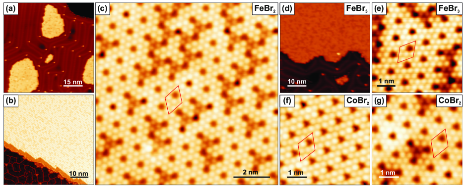
Fig. 1a-c show STM images illustrating the typical morphology of single layer FeBrx films grown in UHV by thermal evaporation of anhydrous FeBr2 and FeBr3 powder on Au(111) kept at 450 K and 390 K, respectively. It is remarkable that the structure of both powders is almost identical, providing direct evidence for non-stoichiometric sublimation. The atomic-resolution STM images reveal a hexagonal lattice with a period of pm, similar to the unit cell of a FeBr2 single crystal with 377.2 pm, [23] which resembles the Br atoms in the top TMD halide layer. In addition to the atomically resolved Br structure, the STM topographies exhibit a well-ordered hexagonal superstructure of dark depressions ( pm in depth in STM) highlighted by the red unit cells. The superstructure has a size of Å and is mostly defect-free over the entire layers. We note the superstructure also formed at room temperature preparations. In addition to the regular superstructure, triangular-shaped irregularities in the top Br lattice are seen, which we attribute to Br-bottom defects and which will be discussed in the next section.
The superstructure can be attributed to either an ordered vacancy lattice or a Moiré pattern caused by the rotation of the FeBr2 lattice with respect to the Au(111) lattice. Generating periodically arranged point defects in 2D materials with this high quality is an extremely challenging task, however, and remains elusive to date.[1, 2] Nevertheless, we assign the occurrence of the superstructure to a periodic Br vacancy lattice for the following reasons: (i) Apart from the non-stoichiometric deposition of FeBr2 and FeBr3 resulting in the same 2D-TMD structures, we frequently observe atomic chains on Au(111) forming a mesh (see Fig. 1b), which we assign to residual Br atoms coexisting to the 2D-TMD islands. Both corroborate a thermal decomposition of the powders during sublimation, leading to Br-deficient 2D-TMD. (ii) The topographic contrast of the superstructure is mostly bias-independent over a large voltage range (-3V to 2 V, see Fig. S2) and also clearly seen in constant-height mode STM and nc-AFM images, which rules out that the superstructure is related to an electronic effect, for instance, an electronic Moiré pattern arising from the rotated TMD with respect to the Au lattice, see discussion about defects below. (iii) Only one atom in the unit cell is recessed from the surface; there is no periodic modulation observed, common for Moiré patterns.
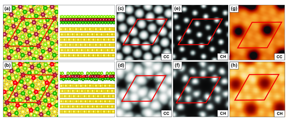
Next, we tried to reproduce the experimental STM images using DFT calculations at the PBE+D3 level using VASP to corroborate the conclusion that the observed superstructures are vacancy lattices in the top halide layer. The unit cell of the pristine FeBr2 structure contains 21 atoms (7 Fe and 14 Br), matching the unit cell of the superstructure observed experimentally. Initially, the pristine and defective 1T-FeBr2 layers were relaxed in the gas phase and subsequently deposited onto the surface using a commensurate unit cell size. As expected, the periodic depressions are not reproduced in calculated STM images of a DFT-optimized pristine 1T-FeBr2 layer on Au(111), see Fig. 2. In fact, the calculated STM image of the pristine FeBr2 layer on Au(111) shows only the atomic corrugation of the Br atoms in the top layer, not even a Moiré pattern, see also Fig S3. In order to identify the most likely point defect causing the periodic depressions in the experimental images, we calculated FeBr2-films with periodic Br-vacancies in the top layer, as the depressions coincide with Br-sites. The simulated constant-current and constant-height STM images show a depression at the Br-vacancy site in good agreement with experimental images, as depicted in Fig. 2c-f. Importantly, introducing the Br vacancies in the top layer leads to a periodic alternation of 5-fold and 6-fold coordinated Fe atoms throughout the films (highlighted by light and dark-colored Fe atoms in Fig. 2a-b, which may lead to intriguing magnetic and electronic properties. Thus, the excellent match between the experimental findings and the simulated STM calculations supports that a Br-vacancy lattice in the top Br-layer of the TMD is formed. We refer to the Br-vacancy lattices as VFeBr2 and VCoBr2, in the following.
Interestingly, the formation of a Br vacancy lattice in the Br top layer is not unique to FeBr2, but was also observed for submonolayers of CoBr2 deposited on the Au(111) kept at 390 K, see Fig. 1f. We note the similarity in lattice parameters between the two TMDs, which may imply that the structures could be stabilized by the mismatch to the Au surface.[19] However, the structure is different for NiBr2, likely because for NiBr2 thermal decomposition is negligible.[8] In the following, we mainly focus on FeBr2.
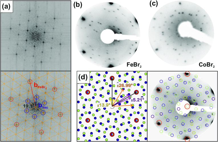
The Br-vacancy superstructure denotes a ( structure with respect to the FeBr2 lattice, as seen by the Fast Fourier transform of an atomically resolved STM image of a VFeBr2 layer in Fig. 3a. Furthermore, the unit cell with is commensurate to the Au lattice as proven by LEED, Fig. 3b-d. We observe a rotation of the superstructure toward the high symmetry axes of Au lattice, as well as a and rotation of the FeBr2 lattice toward the Au lattice (Fig. S7/Fig. S8). Hence, there are four distinct domains with , see Tab. S1, that result in a total of 24 domains, including the ones rotated by multiples of 60∘ with respect to , see Fig. S6. In accordance, the simulated LEED pattern leads to two unique subpatterns shown in blue and green in (Fig. 3d). The simulated LEED fits the experiment perfectly and also confirms that the observed FeBr2 superstructure is commensurate with the underlying Au substrate. Similar LEED patterns for VFeBr2 and VCoBr2 in Fig. 3b-c demonstrate that halogen vacancy lattices can be obtained for several TMDs.
The apparent height of the VFeBr2 monolayers measures 1.80.1 Å (Fig. S10), which is significantly lower compared with the known bulk interlayer spacing of 6.23 Å.[25, 26] The lower apparent height may be explained by the difference in the local density of states of the VFeBr2 and the Au probed by the STM measurements at the applied bias voltage, as also observed for TMDCs on Au(111).[27] Our DFT calculations showed for the pristine FeBr2, FeBr2 with Br top vacancy, and FeBr2 with Br top and bottom vacancy an averaged vertical Br-Br distance between the top and bottom layer of 2.79 Å, 2.75 Å, and 2.68 Å, respectively. The pristine FeBr2 has an averaged adsorption height of 2.91 Å and 4.33 Å for the bottom Br and the Fe atoms above the surface. The herringbone reconstruction of the Au(111) surface is lifted by the VFeBr2 islands, leading to an irregular orientation of the solution lines around the VFeBr2 islands.
II.0.2 Defects in single layer FeBr2 and CoBr2
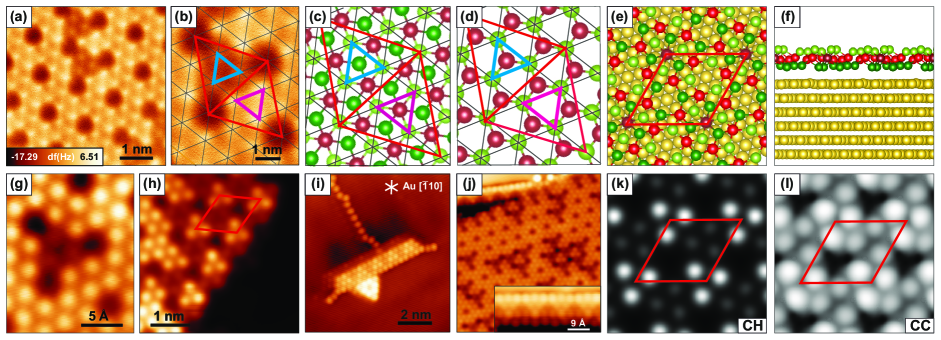
Next, we discuss the Br-vacancies in the top layer and other typical point defects observed in single layers FeBr2 and CoBr2 based on STM and nc-AFM measurements. In the constant-height nc-AFM images of FeBr2, Fig. 4a-b, we assign the hexagonal lattice of bright features (positive frequency shifts) to the outer bromine atoms, which are close enough to the tip to generate repulsive forces, and the darker surrounding and depressions to the lower-lying metal atoms and Br-vacancy, respectively, whose larger distance from the tip resulted in attractive forces, see also Fig. S5. The simulated nc-AFM images based on the DFT-optimized models on Au(111) using the probe particle model with a Br at the tip apex show excellent agreement with the experimental nc-AFM data, see Fig. S4 The nc-AFM data corroborate that the periodic depressions are related to topographic effects, such as vacancies or atoms recessed into the TMD layer. Additionally, we can exclude substitutional defects since Br and Fe atoms possess similar vdW radii. They would result in similar nc-AFM images and are not expected to appear as a depression in the halides lattice.
The triangular-shaped defect, embraced by three Br vacancies and composed of three dimmer atoms surrounding a depression, can be observed in both constant-height STM (Fig. 4g-h) and nc-AFM images with a similar appearance in Fig. 4a-b. This type of defect most frequently occurs and is independent of the preparation conditions of both 2D-TMDs, FeBr2 and CoBr2. The simulated nc-AFM images have revealed that in VFeBr2 single layers, the Br atoms are observed as bright protrusions. Hence, the overlaid lattice in Fig. 4b confirms that the periodic depressions of the superstructure and, likewise also, the three dimmer atoms of the triangular-shaped defect are centered at Br-sites within the halide top layer. Consequently, the dark depression in the center of the triangular-shaped defect is either a Fe vacancy (purple triangle in Fig. 4c) or a Br vacancy (blue triangle in Fig. 4c) in the bottom layer. We note that all the triangular-shaped defects have the same orientation, i.e. are in the same half-unit cell within the layer. Therefore, only one of the proposed defects occurs in the experiment. As the formation energy for halide vacancies is significantly lower than for transition metal or for antisite defects in TMDs,[28] we assign the dark depressions in the center of the triangular defect to vacancies in the Br-bottom layer. This allows the surrounding three top-Br to relax toward the surface, consistent with a lower apparent contrast in constant-height STM and nc-AFM images. We note the triangular-shaped defects can also form clusters near step edges, see Fig. 4h. In conclusion, we dominantly see Br vacancies, in agreement that we observe a decomposition and loss of halogens during the growth of FeBr2, while Fe-based vacancies are very rare, see Fig. S11. Hence we confirm that in VFeBr2, the Fe-sublayer is intact in contrast to FeBr3.
Based on similar reasoning, it can be concluded that VFeBr2 layers exhibit 1T-stacking as opposed to a 1H-stacking. If one assumes a 1H-FeBr2 model, as shown in Fig. 4d, the formation of the triangular defect would require an energetically expensive Fe vacancy, which may not result in the spontaneous formation of the triangular-shaped defects, which we see under all preparation conditions and for all three material systems, i.e. FeBr2, CoBr2, and FeBr3.
Our next step is to simulate the appearance of the bottom layer Br vacancy using DFT calculations. We used the model for the pristine layer and selected the two Br vacancy sites, one in the top and one in the bottom layer, symmetrically positioned within the unit cell, such that both vacancy sites are located over the same Au- adsorption site (top-site). The simulated constant-height and constant-current STM images in Fig. 4k-l show that the three Br in the top layer located around the defect has a reduced apparent height. The observation of a pm lowered adsorption height of the surrounding Br over the Au surfaces in the optimized structure agrees well with the experimental STM images.
We note some of the periodic Br-top-vacancies have a darker contrast ( pm height difference) in constant-current STM experiments, as seen, for example, in Fig. S12. This is likely due to the adsorption of atoms into the vacancy, which can be H from the rest gas in UHV or free Br atoms that are covalently bound to the Au substrate, hence with a lower adsorption height above the surface and not coordinated to Fe. The latter would partially restore the 1:2 (Fe:Br) stoichiometry on the surface
II.0.3 Growth mechanism of VFeBr2
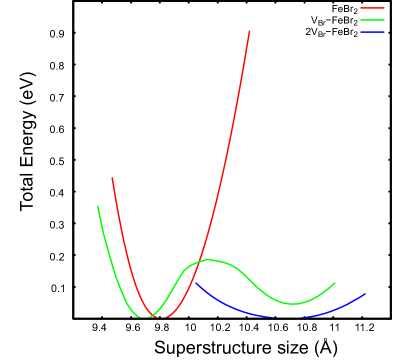
In this section, we show how the observed bromine vacancies in FeBr2 on Au(111) soften the monolayer and provide a possible way to reduce lattice-mismatch strain to the substrate. Importantly, the pristine FeBr2 lattice would need to be stretched by around 4 to fit Au(111). Instead, the occurrence of periodic vacancies can lead to an expansion or compression of the lattice in TMDs,[28] e.g. the interatomic distances between transition metal cations within the layers is 3.69 Å in FeBr3 and 3.78 Å in FeBr2.[25] Therefore, we investigated the softness of the pristine (FeBr2) as well as one- (VFeBr2) and two-(2VFeBr2) Br vacancies in FeBr2 monolayers based on the energetic and structural evolution as a function of biaxial strain using DFT. As compared to the automated unit cell optimization offered by VASP, this approach has an advantage in that it simplifies the identification of multiple potential energy surfaces (PESs) that may exist due to the presence of energetically similar minima. Fig. 5 shows the potential energy for freestanding monolayers as a function of superstructure size. Since the energy continuously varies without abrupt decrease, we can conclude that Fe-Br bonds are not broken, and only elastic deformation of layers is taking place. The pristine FeBr2 and 2VFeBr2 monolayer show a single minimum at 9.81 Å and 10.70 Å, respectively. The VFeBr2 lattice features two local energy minima at 9.68 Å and 10.71 Å corresponding to the equilibrium and a meta-stable state. With an energy difference of less than 100 meV, the meta-stable state is experimentally accessible. Hence, the vacancies soften the FeBr2 layer toward larger unit cell sizes due to incorporating 5-fold coordinated Fe atoms into the lattice. Therefore, the lattice misfit to the relaxed Au cell (10.45 Å) is significantly reduced from the pristine to a meta-stable VFeBr2 from 6.1% to -2.5% and to a 2VFeBr2 lattice to -2.4%, respectively.
In order to better understand the possibility of defect formation in FeBr2 single layers, we calculated the formation energies for Br vacancies in the top and bottom halide layers in gas phase. The calculated formation energy for a single Br vacancy in pristine FeBr2 to obtain VFeBr2 is 45 meV/Br, while for two Br vacancies (one in the top- and one in the bottom halide layer) to get 2VFeBr2 is 56 meV/Br. Hence, the calculated formation energies are comparable to the thermal energy at room temperature, which indicates that the formation of Br defects is energetically feasible. A low formation energy is crucial for the growth of long-range ordered and high-quality vacancy lattices. It agrees well with the experimental observations that a perfect Br-vacancy lattice in the top layer is achieved independent of film size. Only near Au-steps or dislocation lines on Au(111) narrow FeBr2 ribbons are observed without Br-top vacancies, see Fig. 4i-j. The formation of Br vacancies in the bottom halide layer might be diffusion-limited and hence less frequently observed, consistent with that larger islands of 2VFeBr2 are observed along layer edges. The VFeBr2 lattices on Au(111) are stable up to around 470 K, before they desorb intact from the surface. In conclusion, we find that the growth of the periodic vacancy lattice is facilitated by strain engineering at the TMD-gold interface in combination with the low energy costs for Br vacancy formation.
III Discussion
Intrinsically patterned 2D materials are crucial for the selective functionalization by the adsorption of molecules or atoms, as well as tuning their electronic and magnetic properties. While the introduction of periodic Fe vacancies into single-layer FeBr2 leads to the formation of single-layer FeBr3,[29, 30] we achieved the first time the formation of periodic halogen vacancy lattices in TMDs by strain engineering. Importantly, the halogen vacancy lattices offer a way to modulate the coordination number of Fe along the 2D layer and hence alter the charge distribution, while in pristine FeBr3 and FeBr2 the iron coordination is constant in the entire film. We confirm previous results that 2D-FeBr2 is ferromagnetic, see Fig. S9.[19] The change in coordination opens pathways to exotic spin textures with non-collinear spin, which is challenging in pristine 2D-TMDs as their properties are mostly inherited from their vdW bulks and hence have a simple spin texture. Moreover, the first-time intermediate stoichiometric FeBr2 and CoBr2 layers (different from MX2 and MX3) are studied in this work, i.e. Fe7Br13 and Co7Br13. The formation of 2D materials with intrinsic vacancy patterns is likely not exclusive to FeBr2 and CoBr2 on Au(111). Other TMDs and eventually also TMDCs, are likely to exhibit similar patterns, provided that the formation energy of the vacancies is low and the lattice-mismatch strain is appropriately controlled in the respective system.
IV Conclusions
In conclusion, we used low-temperature STM, nc-AFM, LEED, and DFT to identify the structure of single FeBr2 and CoBr2 layers on Au(111). Interestingly, we observe a periodic superstructure of Br vacancies in the top halide layer on both materials. We show that the formation of the regular vacancy lattice is explained by low Br-vacancy formation energy accompanied by an increased softness of the TMD layers and a significant decrease in the lattice-mismatch strain. Despite the large number of transition metal halide and chalcogenide materials available, their periodic patterning in 2D by creating point defects has been elusive so far. The versatile strategy for long-range ordered patterning is crucial for selective functionalization with molecular and atomic species, as well as tuning their electronic and magnetic properties. In particular, as FeBr2 and CoBr2 are 2D ferromagnets, this provides new pathways to create unconventional spin textures with non-collinear spin.
V Experimental Methods
STM and nc-AFM. The STM and nc-AFM measurements were carried out at T = 4.8 K in an ultrahigh vacuum (UHV) system with a base pressure lower than 3 mbar. A commercial STM/nc-AFM (Scienta-Omicron GmbH) equipped with a Nanonis control unit (SPECS GmbH) was used in this work. A qPlus tuning fork sensor[31] ( Nm-1, kHz, ) with a chemically etched tungsten tip was used to acquire most STM and nc-AFM images. For a few STM measurements, a Pt/Ir tip was used. The STM tips were prepared and formed by controlled indentation into the Au(111) surface. For STM, the tip was grounded, and the bias was applied to the sample during the measurements. All bias voltages mentioned in the manuscript refer to the sample bias.
The nc-AFM measurements were recorded in frequency modulation mode, operated at a constant amplitude ( pm). The amplitude was calibrated using the normalized time-averaged tunneling current method. [32, 33] For the nc-AFM experiments, an HF2LI phase-locked loop from Zurich Instruments was used. The tip was grounded during the nc-AFM measurements. The STM and nc-AFM data were processed using the WSxM software.[34]
LEED. The LEED patterns of FeBr2 were acquired using a commercial SpectaLEED from Scienta Omicron, while the CoBr2 samples were measured with an MCP-LEED from OCI Vacuum Microengineering Inc. The LEED patterns are simulated with LEEDPat4.2 software.[35]
Sample preparation. The Au(111) single crystal (MaTeck) was cleaned by several cycles of Argon ion sputtering followed by annealing to 650 K for 15 min. All sample temperature values provided in this manuscript refer to measurements at a thermocouple that is located in close proximity to the sample. The FeBr2 (Iron(II) bromide, anhydrous, purity 98%, Alfa Aesar), FeBr3 (Iron(III) bromide, anhydrous, purity 98%, Alfa Aesar) and CoBr2 (Cobalt(II) bromide, anhydrous, purity 97%, Alfa Aesar) powders were evaporated in UHV from a Knudsen cell (Kentax GmbH) located in the preparation chamber. The sublimation from a quartz crucible occurred at 550 K (FeBr2/FeBr3) and 590 K (CoBr2) at an evaporation pressure of around 10-9 mbar. During deposition, the Au(111) sample was kept at 390 K-450 K, the temperatures are indicated in the respective figure captions. The deposition rate of FeBr2, FeBr3 and CoBr2 was checked by a quartz microbalance and the powders were thoroughly degassed respectively before the sublimation to Au(111). The deposition rate of FeBr2, FeBr3 and CoBr2 used in this work are 0.02-0.07 ML/min, respectively. The coverage of the FeBr2 film was controlled by varying the evaporation time.
Calculations. The first principles calculations reported here are performed within the framework of the density functional theory (DFT), employing the VASP code.[36, 37] In the periodic VASP calculations, the projector augmented wave (PAW)[38] method was employed to describe the core electrons. The exchange-correlation energy and potential are treated within the spin-polarized generalized gradient approximation (GGA) using the exchange-correlation functional of Perdew-Burke-Ernzerhof (PBE)[39] with the DFT-D3 dispersive corrections[40] (using Becke-Johnson damping). The energy cutoff for the plane wave is kept at 400 eV for the ground state calculations. Energies were converged to 10-5 eV and geometries were relaxed until the forces on all atoms were below 0.001 eV/Å, respectively. A Methfessel-Paxton-smearing [41] of first order with smearing parameter =0.2 eV was used. To model the FeBr2 structures in the gas phase and on the substrate, we have constructed a superstructure corresponding to a on domain. The pristine FeBr2 structure contains 21 atoms (7 Fe and 14 Br atoms). The gold slab consists of six layers, with the bottom three layers fixed to the bulk geometry and the remaining three layers free to relax. To prevent interactions between the slab and its periodic images and to account for the finite size of the slab model, gas phase systems were computed with 16 Å of vacuum space and surface calculations were computed with 30 Å of vacuum space in the -direction. A set of (661) centered k-point sampling are used for both gas phase and surface calculations.
The formation energy Efor of defects is calculated using the equation Efor=Edefective - E + , [28] where Edefective and E represent the total energy of the defective and pristine FeBr2 single layers, and ni and are the number and chemical potential of the removed atom, respectively. To calculate , we use the relation Fe + 2Br, where Fe, Br, and are the total energies of Fe, Br, and single-layer FeBr2. For calculating Fe, we assume the stable bulk form of Fe(bcc-Fe) at the Fe-rich limit.[19] Hence, Br can be evaluated from Fe-bulk and the total energy of single-layer FeBr2.
Constant-height and constant-current STM images were simulated within the Tersoff–Hamann model.[42, 43] The tip was placed Å over the plane of the top Br layer for constant-height images at different bias voltages. For the constant-current STM images, the isodensity values are adjusted from 10-3 to 114 electron/Å3. Constant-height nc-AFM simulations were based on the probe particle model established by Hapala, et al. [44] and widely used to model the nc-AFM imaging process with functionalized tips. We assumed a Br at the tip apex as the tip was intentionally crashed softly into the FeBr2 monolayer. Frequency shift images were calculated for the Br-functionalized tip assuming a harmonic spring stiffness of 0.5 N/m and an effective charge of for the probe particle.
V.1 Acknowledgements
This work was funded by the German Research Foundation (DFG) through the SFB 953 Synthetic Carbon Allotropes (project number 182849149) and the Interdisciplinary Center for Molecular Materials (ICMM) at the Friedrich-Alexander-Universität Erlangen-Nürnberg. We thank Andreas Dörr, Dengyuan Li and Sajjan Mohammad for their experimental support and discussions.
V.2 Notes
We became aware that in a recently published preprint, similar STM measurements of FeBr2 on Au(111) were presented.[45] However, a different conclusion concerning the structure and chemical composition was reached.
References
- Feng et al. [2016] B. Feng, J. Zhang, Q. Zhong, W. Li, S. Li, H. Li, P. Cheng, S. Meng, L. Chen, and K. Wu, Experimental realization of two-dimensional boron sheets, Nat. Chem. 8, 563 (2016).
- Lin et al. [2017] X. Lin, J. C. Lu, Y. Shao, Y. Y. Zhang, X. Wu, J. B. Pan, L. Gao, S. Y. Zhu, K. Qian, Y. F. Zhang, D. L. Bao, L. F. Li, Y. Q. Wang, Z. L. Liu, J. T. Sun, T. Lei, C. Liu, J. O. Wang, K. Ibrahim, D. N. Leonard, W. Zhou, H. M. Guo, Y. L. Wang, S. X. Du, S. T. Pantelides, and H. J. Gao, Intrinsically patterned two-dimensional materials for selective adsorption of molecules and nanoclusters, Nat. Mater. 16, 717 (2017).
- He et al. [2021] F. He, Y. Zhou, Z. Ye, S.-H. Cho, J. Jeong, X. Meng, and Y. Wang, Moiré patterns in 2D materials: A review, ACS Nano 15, 5944 (2021).
- Gong et al. [2017] C. Gong, L. Li, Z. Li, H. Ji, A. Stern, Y. Xia, T. Cao, W. Bao, C. Wang, Y. Wang, Z. Q. Qiu, R. J. Cava, S. G. Louie, J. Xia, and X. Zhang, Discovery of intrinsic ferromagnetism in two-dimensional van der Waals crystals, Nature 546, 265 (2017).
- Huang et al. [2017] B. Huang, G. Clark, E. Navarro-Moratalla, D. R. Klein, R. Cheng, K. L. Seyler, D. Zhong, E. Schmidgall, M. A. McGuire, D. H. Cobden, W. Yao, D. Xiao, P. Jarillo-Herrero, and X. Xu, Layer-dependent ferromagnetism in a van der Waals crystal down to the monolayer limit, Nature 546, 270 (2017).
- Wang et al. [2022] Q. H. Wang, A. Bedoya-Pinto, M. Blei, A. H. Dismukes, A. Hamo, S. Jenkins, M. Koperski, Y. Liu, Q.-C. Sun, E. J. Telford, H. H. Kim, M. Augustin, U. Vool, J.-X. Yin, L. H. Li, A. Falin, C. R. Dean, F. Casanova, R. F. L. Evans, M. Chshiev, A. Mishchenko, C. Petrovic, R. He, L. Zhao, A. W. Tsen, B. D. Gerardot, M. Brotons-Gisbert, Z. Guguchia, X. Roy, S. Tongay, Z. Wang, M. Z. Hasan, J. Wrachtrup, A. Yacoby, A. Fert, S. Parkin, K. S. Novoselov, P. Dai, L. Balicas, and E. J. G. Santos, The magnetic genome of two-dimensional van der Waals materials, ACS Nano 16, 6960 (2022).
- Jiang et al. [2023] S. Jiang, G. Wang, H. Deng, K. Liu, Q. Yang, E. Zhao, L. Zhu, W. Guo, J. Yang, C. Zhang, H. Wang, X. Zhang, J.-F. Dai, G. Luo, Y. Zhao, and J. Lin, General synthesis of 2D magnetic transition metal dihalides via trihalide reduction, ACS Nano 17, 363 (2023).
- Bikaljevic et al. [2021] D. Bikaljevic, C. Gonzalez-Orellana, M. Pena-Diaz, D. Steiner, J. Dreiser, P. Gargiani, M. Foerster, M. A. Nino, L. Aballe, S. Ruiz-Gomez, N. Friedrich, J. Hieulle, L. Jingcheng, M. Ilyn, C. Rogero, and J. I. Pascual, Noncollinear magnetic order in two-dimensional NiBr2 films grown on Au(111), ACS Nano 15, 14985 (2021).
- Zhou et al. [2020] X. Zhou, B. Brzostowski, A. Durajski, M. Liu, J. Xiang, T. Jiang, Z. Wang, S. Chen, P. Li, Z. Zhong, A. Drzewiński, M. Jarosik, R. Szczęśniak, T. Lai, D. Guo, and D. Zhong, Atomically thin 1T-FeCl2 grown by molecular-beam epitaxy, J. Phys. Chem. C 124, 9416 (2020).
- Cai et al. [2021] X. Cai, Z. Xu, S.-H. Ji, N. Li, and X. Chen, Molecular beam epitaxy growth of iodide thin films, Chin. Phys. B 30, 028102 (2021).
- Cai et al. [2020] S. Cai, F. Yang, and C. Gao, FeCl2 monolayer on HOPG: art of growth and momentum filtering effect, Nanoscale 12, 16041 (2020).
- Liu et al. [2020] H. Liu, X. Wang, J. Wu, Y. Chen, J. Wan, R. Wen, J. Yang, Y. Liu, Z. Song, and L. Xie, Vapor deposition of magnetic van der Waals NiI2 crystals, ACS Nano 14, 10544 (2020).
- Zhou et al. [2022] X. Zhou, Z. Wang, H. Zhu, Z. Liu, Y. Hou, D. Guo, and D. Zhong, Epitaxial growth and electronic properties of an antiferromagnetic semiconducting VI2 monolayer, Nanoscale 14, 10559 (2022).
- Shcherbakov et al. [2018] D. Shcherbakov, P. Stepanov, D. Weber, Y. Wang, J. Hu, Y. Zhu, K. Watanabe, T. Taniguchi, Z. Mao, W. Windl, J. Goldberger, M. Bockrath, and C. N. Lau, Raman spectroscopy, photocatalytic degradation, and stabilization of atomically thin chromium tri-iodide, Nano Lett. 18, 4214 (2018).
- Mastrippolito et al. [2021] D. Mastrippolito, L. Ottaviano, J. Wang, J. Yang, F. Gao, M. Ali, G. D’Olimpio, A. Politano, S. Palleschi, S. Kazim, R. Gunnella, A. Di Cicco, A. Sgarlata, J. Strychalska-Nowak, T. Klimczuk, R. J. Cava, L. Lozzi, and G. Profeta, Emerging oxidized and defective phases in low-dimensional CrCl3, Nanoscale Adv. 3, 4756 (2021).
- Bergeron et al. [2021] H. Bergeron, D. Lebedev, and M. C. Hersam, Polymorphism in post-dichalcogenide two-dimensional materials, Chem. Rev. 121, 2713 (2021).
- Han et al. [2023] X. Han, J.-Y. You, S. Wu, R. Li, Y. P. Feng, K. P. Loh, and X. Zhao, Atomically unveiling an atlas of polytypes in transition-metal trihalides, J. Am. Chem. Soc. 145, 3624 (2023).
- Ghosh et al. [2021] R. K. Ghosh, A. Jose, and G. Kumari, Intrinsic spin-dynamical properties of two-dimensional half-metallic FeX2 (X = Cl, Br, I) ferromagnets: Insight from density functional theory calculations, Phys. Rev. B 103, 054409 (2021).
- Kulish and Huang [2017] V. V. Kulish and W. Huang, Single-layer metal halides MX2 (X=Cl, Br, I): Stability and tunable magnetism from first principles and monte carlo simulations, J. Mater. Chem. C 5, 8734 (2017).
- Mak et al. [2019] K. F. Mak, J. Shan, and D. C. Ralph, Probing and controlling magnetic states in 2D layered magnetic materials, Nat. Rev. Phys. 1, 646 (2019).
- Feng et al. [2018] Y. Feng, X. Wu, J. Han, and G. Gao, Robust half-metallicities and perfect spin transport properties in 2d transition metal dichlorides, J. Mater. Chem. C 6, 4087 (2018).
- Botana and Norman [2019] A. S. Botana and M. R. Norman, Electronic structure and magnetism of transition metal dihalides: Bulk to monolayer, Phys. Rev. Mater. 3, 044001 (2019).
- Wilkinson et al. [1959] M. K. Wilkinson, J. W. Cable, E. O. Wollan, and W. C. Koehler, Neutron diffraction investigations of the magnetic ordering in FeBr2, CoBr2, FeCl2, and CoCl2, Phys. Rev. 113, 497 (1959).
- Sojka et al. [2013] F. Sojka, M. Meissner, C. Zwick, R. Forker, and T. Fritz, Determination and correction of distortions and systematic errors in low-energy electron diffraction, Rev. Sci. Instrum. 84, 015111 (2013).
- McGuire [2017] M. A. McGuire, Crystal and magnetic structures in layered, transition metal dihalides and trihalides, Crystals 7, 121 (2017).
- Haberecht et al. [2001] J. Haberecht, H. Borrmann, and R. Kniep, Refinement of the crystal structure of iron dibromide, FeBr2, Z. Kristallogr. N. Cryst. Struct. 216, 544 (2001).
- Tumino et al. [2019] F. Tumino, C. S. Casari, M. Passoni, V. Russo, and A. Li Bassi, Pulsed laser deposition of single-layer MoS2 on Au(111): from nanosized crystals to large-area films, Nanoscale Adv. 1, 643 (2019).
- Ceyhan et al. [2021] E. Ceyhan, M. Yagmurcukardes, F. M. Peeters, and H. Sahin, Electronic and magnetic properties of single-layer FeCl2 with defects, Phys. Rev. B 103, 014106 (2021).
- Miro et al. [2014] P. Miro, M. Audiffred, and T. Heine, An atlas of two-dimensional materials, Chem. Soc. Rev. 43, 6537 (2014).
- Ashton et al. [2017] M. Ashton, J. Paul, S. B. Sinnott, and R. G. Hennig, Topology-scaling identification of layered solids and stable exfoliated 2D materials, Phys. Rev. Lett. 118, 106101 (2017).
- Giessibl [2000] F. J. Giessibl, Atomic resolution on Si(111)-(7×7) by noncontact atomic force microscopy with a force sensor based on a quartz tuning fork, Appl. Phys. Lett. 76, 1470 (2000).
- Simon et al. [2007] G. H. Simon, M. Heyde, and H.-P. Rust, Recipes for cantilever parameter determination in dynamic force spectroscopy: spring constant and amplitude, Nanotechnology 18, 255503 (2007).
- Sugimoto et al. [2010] Y. Sugimoto, Y. Nakajima, D. Sawada, K.-i. Morita, M. Abe, and S. Morita, Simultaneous afm and stm measurements on the surface, Phys. Rev. B 81, 245322 (2010).
- Horcas et al. [2007] I. Horcas, R. Fernandez, J. M. Gomez-Rodriguez, J. Colchero, J. Gomez-Herrero, and A. M. Baro, WSXM: a software for scanning probe microscopy and a tool for nanotechnology, Rev. Sci. Instrum. 78, 013705 (2007).
- [35] K. Hermann and M. van Hove, LEEDpat4 (LEED pattern analyzer).
- Kresse and Furthmüller [1996] G. Kresse and J. Furthmüller, Efficient iterative schemes for ab initio total-energy calculations using a plane-wave basis set, Phys. Rev. B 54, 11169 (1996).
- Kresse and Furthmüller [1996] G. Kresse and J. Furthmüller, Efficiency of ab-initio total energy calculations for metals and semiconductors using a plane-wave basis set, Comput. Mater. Sci. 6, 15 (1996).
- Blöchl [1994] P. E. Blöchl, Projector Augmented-Wave Method, Phys. Rev. B 50, 17953 (1994).
- J.P. Perdew [1996] M. E. J.P. Perdew, K. Burke, Generalized gradient approximation made simple, Phys. Rev. Lett. 77, 3865 (1996).
- Grimme et al. [2010] S. Grimme, J. Antony, S. Ehrlich, and H. Krieg, A consistent and accurate ab initio parametrization of density functional dispersion correction (DFT-D) for the 94 elements H-Pu, J. Chem. Phys. 132, 154104 (2010).
- Methfessel and Paxton [1989] M. Methfessel and A. T. Paxton, High-Precision Sampling for Brillouin-Zone Integration in Metals, Phys. Rev. B 40, 3616 (1989).
- Tersoff and Hamann [1983] J. Tersoff and D. R. Hamann, Theory and application for the scanning tunneling microscope, Phys. Rev. Lett. 50, 1998 (1983).
- Tersoff and Hamann [1985] J. Tersoff and D. R. Hamann, Theory of the scanning tunneling microscope, Phys. Rev. B 31, 805 (1985).
- Hapala et al. [2014] P. Hapala, G. Kichin, C. Wagner, F. S. Tautz, R. Temirov, and P. Jelínek, Mechanism of high-resolution STM/AFM imaging with functionalized tips, Phys. Rev. B 90, 085421 (2014).
- Hadjadj et al. [2023] S. E. Hadjadj, C. Gonzalez-Orellana, J. Lawrence, D. Bikaljevic, M. Pena-Diaz, P. Gargiani, L. Aballe, J. Naumann, M. A. Nino, M. Foerster, S. Ruiz-Gomez, S. Thakur, I. Kumberg, J. Taylor, J. Hayes, J. Torres, C. Luo, F. Radu, D. G. de Oteyza, W. Kuch, J. I. Pascual, C. Rogero, and M. Ilyn, Epitaxial monolayers of magnetic 2d semiconductor FeBr2 grown on Au(111) (2023), arXiv:2304.11972 [cond-mat.mtrl-sci] .