Thermo-electric history effects and resistive switching in epitaxial thin film of Mott insulator V2O3
Abstract
We report interesting thermo-electric history effects associated with an electric field-induced first order phase transition from Mott-insulator to the metallic state in the epitaxial thin film of V2O3. This phase transition results in tuneable resistive switching in V2O3. These findings are promising for novel technologies like optoelectronics and neuromorphic computing and may lead to highly energy-efficient switching applications of Mott insulators.
The archetypal Mott-insulator V2O3 undergoes a transition from a paramagnetic metallic state to a low-temperature antiferromagnetic insulating state around a temperature 160 k imada . This is a first order phase transition (FOPT) arising out of a thermally perturbed balance of entropy, kinetic energy, and Coulomb repulsion among conduction electrons imada ; rozen , and leads to an abrupt electron localization stewart . The Mott transition is also accompanied by a structural change from a high-temperature corundum lattice to a low-temperature monoclinic lattice structure imada . McLeod et al macl studied the real-space evolution of the insulator-metal transition in a thin-film V2O3 sample by high spatial-resolution imaging with the help of a cryogenic near-field infrared microscopy. They observed spontaneously nanotextured coexistence of metal and Mott insulator phases in the temperature regime ( 160-180 K) macl .
Here we report interesting thermo-electric irreversibility associated with the electric-field induced FOPT in an epitaxial thin film of V2O3. Beyond a critical electric field, the sample shows a tunable memory effect, which depends on the temperature and electric field cycle. This memory effect is robust, and thus it is possible to use such V2O3 as a two-port tunable electrical switching device.
The V2O3 thin film was deposited on (222) Al2O3 substrate using the Pulse Laser deposition (PLD) method. A sintered V2O5 pellet was used as a target and 248nm KrF pulse Excimer laser of pulse energy 2J/cm2 and repetition rate 3 Hz was used for deposition. Sapphire (Al2O3) substrate was kept at a distance of 5 cm from the target. During deposition substrate temperature was 6500C and the deposition chamber was evacuated to 10-6 mbar. After deposition, the sample was cooled down to room temperature with 2.2K/min cooling rate while maintaining the same pressure of 10-6 mbar.
The V2O3 thin film was characterized using x-ray diffraction (XRD), X-ray reflectivity (XRR), and Raman spectroscopy. XRD -2 and phi-scan measurements were performed using PAN analytical X’PERT high-resolution x-ray diffraction system equipped with a Cu anode. Raman measurements were performed using Horiba Jobin-Yvon, France, micro Raman spectrometer equipped with a 633 nm excitation laser, 1800 g/mm grating, an edge filter for Rayleigh line rejection and a CCD detector giving a spectral resolution of 1cm-1. The Laser was focused to a spot size of 1 micron onto the surface of the sample using a 50 objective lens. The spectra were collected in backscattering geometry.
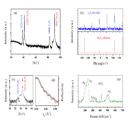
Fig.1(a) presents out-of-plane XRD -2 scan, which reveals the (222) and (444) peaks of V2O3, thus indicating that the film is grown along (222) direction of the rhombohedral R-3c structure on sapphire (222) substrate. The position of the (222) and (444) peaks matched with the bulk counterpart, indicating that the film is nearly relaxed in nature. In-plane epitaxy is further confirmed using an asymmetric phi scan on (321) reflection. Fig.1(b) shows the phi scan on V2O3 thin film along with the phi scan of Al2O3 substrate. The six-fold reflection of substrate and film at the same phi angle indicates the hetero-epitaxial nature of the film. Fig.1(c) presents the in-plane XRD -2 scan around the (321) plane. We have estimated the thickness of the film with the help of XRR study. Uniform deposition of the film is indicated by distinct oscillations observed in XRR pattern (Fig.1(d)). We estimated film thickness to be 70nm from the fitting of the XRR pattern. The microstructure of the deposited thin film V2O3 was further checked with a micro Raman spectroscopy study at room temperature (Fig.1(e)). From group theory, 2Ag+5Eg are the only Raman active modes in the rhombohedral crystal structure of V2O3. Positions of the Ag (238, 502 cm-1) and Eg modes (210, 294, 334 cm-1) agreed well with the previous reports of Raman spectroscopy study in V2O3 tat ; shvets . In the present case, only three Eg modes are visible, and the remaining two Eg modes are not detected due to the very small intensity. Mode at 417 cm-1 originates from the substrate Al2O3 substrate zoub .
We have studied temperature-dependent resistivity and V-I characteristics of the V2O3 thin film in the linear four-point probe configuration, using Keithley 2425 source meter and Keithley 2002 multimeter. The sample temperature was controlled using a Lakeshore 335 temperature controller. Temperature-dependent resistivity measurements in cooling and heating cycles were performed in the temperature sweep mode with 2K/min temperature sweep rate. Isothermal V-I characteristics were obtained in continuous increment/decrement of current and measuring the corresponding voltage difference between two probe points. For measuring the isotherm at a particular temperature, each time sample was cooled from 250K with a cooling rate of 5K/minute. For a special electric field cooled isothermal V-I characteristics measurement at 6.3K, the sample was cooled down from 250 K in the presence of an applied 0.15A dc current. After reaching the 6.3 K, isotherm was obtained after reducing the current to zero and then varying it in the sequence 0 A 0.15A 0 A - 0.15 A 0 A. To check the effect of joule heating, the measurements were also performed in pulsed current mode. The results obtained are quite similar in both the modes and thus rule out any significant role of the joule heating.
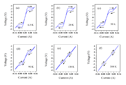
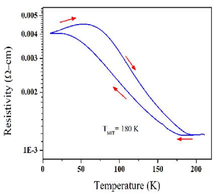
Fig 2 presents temperature dependence of resistivity in V2O3 thin film between 210 K and 5 K. With decreasing temperature, the sample undergoes a metal-to-insulator transition around 180 K. This Mott transition temperature agrees well with the values reported in the literature both for bulk and thin film samples of V2O3 imada ; macl . The transition is marked with a distinct and broad thermal hysteresis, which is the hallmark of a disordered influenced first order phase transition sbroy1 ; sbroy2 . There is a structural change associated with the Mott metal-insulator transition in V2O3 imada . Raman spectroscopy study at various temperatures below the Mott transition temperature confirmed the same in our present thin film V2O3 sample binoy .
The electric field-driven formation of a conductive state in a conventional band insulating system is based on the well-known Landau-Zener mechanism of quantum tunneling across the insulating band gap zener . The rigid band gap is determined by the chemical composition and lattice structure of the materials, which needs to be overcome by the applied electric field. This sets a lower bound of the threshold electric field and limits the density of excited carriers promoted across the gap. Mott insulators with the collective nature of their gap can be ideal candidates to overcome this limit and provide a potential alternative to band semiconductor-based microelectronics. In recent times electrically triggered insulator-to-metal transition in various Mott insulators has drawn much interest mazza ; valm ; kolch . To investigate the possibility of electrically driven Mott insulator to metal transition in the present V2O3 sample, in Fig 3 we present isothermal V-I curves obtained at various temperatures both above and below the Mott transition temperature. The V-I curve at T = 300 K shows the typical linear metallic behaviour. This behaviour starts changing below the Mott transition temperature with the appearance of distinct non-linearity in the V-I characteristic accompanied by a hysteris loop beyond a threshold of applied current. This threshold current increases with the decrease in temperature, and so does the linearity and the associated hysteresis. As mentioned above we have repeated some of these measurements by applying the current in pulsed mode, and we observed qualitatively the same behaviour. Thus the observed non-linearity and the associated irreversibility are robust and reproducible in different experimental cycles. Below the threshold current, the V-I curves are linear and reversible at all temperatures. Thus the observed features can be utilized to build a volatile electrical resistive switching device.
There are two competing mechanisms namely a purely electronic mechanism and an electro-thermal mechanism to explain the electric field-driven insulator to metal phase transition in Mott insulators mazza ; valm ; kolch ; valle . Mazza et al mazza with the help of dynamical mean-field theory argued that the electric breakdown of the Mott insulator occurred via a Mott insulator to metal FOPT characterized by an abrupt gap collapse. They showed that within the insulator-metal coexistence region, an electric field could drive a discontinuous transition from the insulator to a gap-collapsed metal at the threshold electric fields much smaller than those expected in a Zener breakdown. In the region away from insulator-metal coexistence, the electric breakdown occurs through a more conventional quantum tunneling across the Hubbard bands tilted by the electric field. This work established a framework to understand the metallization of a Mott insulator, where the electric field drives a FOPT from the correlated Mott insulator to a gap-collapsed metal phase, preexisting as a metastable state at zero fields. McLeod et al macl experimentally established such spontaneously nanotextured coexistence of metal and correlated Mott insulator phases near the insulator to metal transition (around 160-180 K) associated with percolation in V2O3. It may be noted that such phase-coexistence is a universal feature of a disorder-influenced FOPT in general, and has been studied extensively in various classes of magnetic materials sbroy1 . Such a temperature and magnetic field driven disorder-influenced FOPT with its associated features (phase coexistence, thermomagnetic irreversibility etc.) can give rise to various kinds of functionalities namely giant magneto-caloric effect, magnetostriction, magnetic shape memory effect, magnetic memory etc sbroy1 . del Valle et al valle argued that the Mott insulator to metal transition in V2O3 could be triggered directly by the electric field, possibly by carrier injection into the conduction band and destabilization of the insulating phase. Joule heating can occur in these metallic hotpots to cause an increase in local temperature and further metallization. While Joule heating can subsequently play a role in the growth and percolation of the metallic phase, it is not the primary cause of metallization. In our present experiment, we have ruled out the primary role of Joule heating by repeating some experiments in pulsed current mode. Furthermore, we have separately checked the increase in the temperature of the sample on application of a current of 0.15 A by putting a temperature sensor very near to the sample after stabilizing the temperature at 6.3 K. The observed rise in the temperature was to 6.4 K. However, irrespective of the starting mechanism and subsequent dominant role in the switching, whether it is the electric field-effect or Joule heating, or a combination of both effects, the observed electric field-driven switching in the present thin film of V2O3 is very robust and experimentally reproducible.
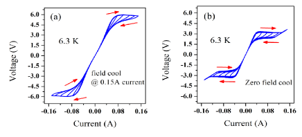
FOPT in various magnetic systems are associated with very interesting thermo-magnetic hysteresis and memory effects sbroy1 . Taking a cue from such study, we have measured V-I characteristic of the present thin film V2O3 sample at T = 6.3 K after cooling the sample from room temperature in the presence of an applied current of 0.15 A. Furthermore, we have drawn minor hysteresis loops by limiting the applied current to various values less than the maximum applied current of 0.15 A. We present these V-I curves with minor hysteresis loops in Fig. 4 at T = 6.3 K obtained in a current-cooled mode and also in the conventional zero current-cooled mode. First of all akin to the magnetic systems, there is a distinct difference between the V-I curves obtained in current-cooled and zero current-cooled modes. Furthermore, the minor hysteresis loops provide the macroscopic evidence of the phase coexistence in a disorder broadened first order phase transition (see reference sbroy1 and references therein), which in the present case is initiated by an electric field. These memory effects can be suitably utilized for memory applications. Relatively low power ( ¡ 1 W) requirement for observing various interesting features, makes this thin film V2O3 even more suitable for applications.
In summary, the electric field-driven correlated Mott-insulator to metal transition and the associated thermo-electric memory effects result in volatile resistive switching in V2O3 and possibilities of memory applications. Thus it is a promising candidate for novel technologies like optoelectronics liu ; but and neuromorphic computing pickett ; zhou ; kumar .
The authors have no conflicts to disclose.
Binoy Dey and S. B. Roy acknowledge financial support obtained from the Raja Ramanna Fellowship program sponsored by DAE, Government of India.
References
- (1) M. Imada, A. Fujimori and Y. Tokura, Rev. Mod. Phys. 70, 1039 (1998).
- (2) M. J. Rozenberg et al. Phys. Rev. Lett. 75, 105 (1995).
- (3) M. K. Stewart et al. Phys. Rev. B 85, 205113 (2012).
- (4) A. S. McLeood et al, Nature Physics, 13 80 (2016).
- (5) C. Tatsuyama and H. Y. Fan, Phys. Rev. B 21, 2977 (1980).
- (6) P. Shvets et al, J Raman Spectrosc. 50 1226 (2019).
- (7) E. Zouboulis; D. Renusch; M. Grimsditch, Appl. Phys. Lett. 72, 1 (1998).
- (8) S. B. Roy, J. Phys.: Condensed Matter 25 183201 (2013)
- (9) S. B. Roy, Mott Insulators: Physics and Applications (IOP Publishing, UK, 2019).
- (10) Binoy De, V. Sathe and S. B. Roy (to be published).
- (11) C. Zener, Proc. R. Soc. A 145, 523 (1934).
- (12) G. Mazza et al, Phys. Rev. Lett. 117, 176401 (2016).
- (13) I. Valmianski et al, Phys. Rev. B 98, 195144 (2018).
- (14) Yoav Kalcheim et al, Nature Commun. 11 1985 (2020). https://doi.org/10.1038/s41467-020-16752-1
- (15) J. del Valle et al., Science 373, 907 (2021)
- (16) M. Liu et al., Nature 487, 345 (2012).
- (17) N. A. Butakov et al., ACS Photonics 5, 4056 (2018).
- (18) M. D. Pickett, G. Medeiros-Ribeiro, R. S. Williams, Nat. Mater. 12, 114 (2013).
- (19) Y. Zhou, S. Ramanathan, Proc. IEEE 10, 1289 (2015).
- (20) S. Kumar, J. P. Strachan, R. S. Williams, Nature 548, 318 (2017).