,,
Thin channel Ga2O3 MOSFET with 55 GHz fMAX and >100 V breakdown
Abstract
This letter reports a highly scaled 90 nm gate length -Ga2O3 (Ga2O3) T-gate MOSFET with power gain cut off frequency (fMAX) of 55 GHz. The 60 nm thin epitaxial Ga2O3 channel layer was grown by molecular beam epitaxy (MBE) while the highly doped (n++) source/drain regions were regrown using metal organic chemical vapour deposition (MOCVD). Maximum on current (IDS, MAX) of 160 mA/mm and trans-conductance (gm) around 36 mS/mm was measured at VDS = 10 V for LSD = 1.5 m device. Transconductance and on current are limited by high channel sheet resistance (Rsheet). Gate-drain breakdown voltage of 125 V was measured for LGD = 1.2 m. We extracted 27 GHz current gain cut-off frequency (fT) and 55 GHz fMAX for 20 V drain bias for unpassivated devices. The reported fMAX is the highest for Ga2O3. While no current collapse was seen initially for both drain and gate lag measurements for 500 ns pulse, moderate current collapse was observed after DC, RF measurements caused by electrical stressing. No large signal RF data was extracted due to a lack of proper tuning of the input (high S11) in the load-pull setup. However, after repeated DC and large signal measurement trials, we found that both fT and fMAX degraded significantly which was correlated to high-frequency gm collapse. Despite this, we calculated a high fT. VBR product of 3.375 THz.V which is comparable with state-of-art GaN HEMTs. This figure of merit suggests that Ga2O3 could be a potential candidate for X-band application.
-Ga2O3 (Ga2O3) is an ultrawide bandgap semiconductor with favorable materials propertiesGreen et al. (2022) for next-generation power and RF applications. The predicted breakdown field (8 MV/cm)Green et al. (2022, 2016) and calculated saturation velocityGhosh and Singisetti (2017) supports the candidacy of Ga2O3 for high-frequency switching and high power RF amplifier applications. -Ga2O3 MOSFETs with multi-kV breakdown voltages have been reported Zeng, Vaidya, and Singisetti (2018); Tetzner et al. (2019); Bhattacharyya et al. (2022); Zhang et al. (2022); Farzana et al. (2021), while heterostructure FET (HFET), and diodes with average breakdown field strength of 5.5 MV/cmKalarickal et al. (2021); Saha et al. (2023) has been reported demonstrating the maturity of the technology. Modulation doped -(AlxGa1-x)2O3/Ga2O3 HFET Zhang et al. (2018a) and highly scaled (< 200 nm) MOSFETsChabak et al. (2018) and MESFETs Xia et al. (2019) have been demonstrated to showcase the high-frequency performance. In our previous works, we reported fT = 30 GHz in AlGaO/GaO HFETsVaidya, Saha, and Singisetti (2021); Saha, Vaidya, and Singisetti (2022) and fMAX= 48 GHz using scaled T gate MOSFETSaha et al. (2023). Large signal RF performance has been published for L- band Moser et al. (2020). However, fMAX > 50 GHz is necessary for S and X band applications.
It is necessary to reduce the parasitic source resistance to achieve higher frequencies. The contact regrowth process has been reported in gallium oxide FETsVaidya, Saha, and Singisetti (2021); Saha, Vaidya, and Singisetti (2022); Saha et al. (2023) as an effective way to to reduce contact resistance. In our previous report, we found high regrowth interface resistanceSaha et al. (2023) limiting device performance by increasing source resistance. Careful surface treatment could reduce this regrowth interface resistance problem. Traps in the gate and gate-drain access region can limit device RF performance by introducing current collapse known as DC-RF dispersion Saha et al. (2023). Ex-situ passivation can eliminate the access region traps but traps under the gate are unaffected by passivation Vaidya and Singisetti (2021).
In this letter, we report highly scaled 90 nm T-gate Ga2O3 MOSFET with improved MOCVD contact regrowth process to reduce the interface resistance. Pre-cleaning of the wafer before low-temperature n++ regrowth gave lower interface resistacne. We used atomic layer deposited Al2O3 as the gate dielectric, no current collapse was observed in unpassivated devices. As a result, a peak fT of 27 GHz and fMAX = 55 GHz is obtained in these devices. With a gate-to-drain breakdown voltage of 120 V, the device shows fMAX = 55 GHz and breakdown voltage (VBR) > 100 V which has been reported only in a few state-of-art AlGaN/GaN HFETs Zhang et al. (2018b); Ranjan et al. (2014); Medjdoub et al. (2013).
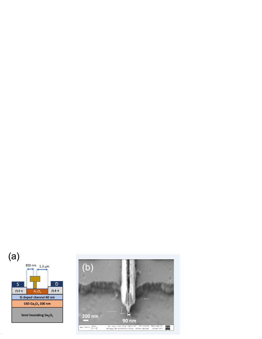
The device layers and structure is shown in Fig. 1 (a). The growth details and device fabrication process is described in detail in previous reports Saha et al. (2023); Vaidya et al. (2019). Before regrowth, the sample was submerged in 1:3 HCl:DI water solution for 15 minutes to remove any atmospheric contaminants Bhattacharyya et al. (2022). Next, 80 nm highly Si doped (1 X 1020 cm-3) n++ layer was grown using MOCVD at a lower 650 0C. Unlike the previous reportSaha et al. (2023), a 20 nm aluminum oxide gate dielectric was used in these MOSFETs. SEM image of the device is shown in Fig. 1 (b), a T-gate was used to improve the gate resistance.
From the capacitance-voltage characteristics (Supplementary material), a sheet carrier charge density (2.9 x 1012 cm-2) was extracted. Transfer length method (TLM) on n++ regrowth layer gave a 0.045 mm lateral contact resistance (Rc,n++) between metal and n++ layer and a sheet resistance (Rsheet,n++) of 181 /. TLM structure on n++ layer through the channel was also fabricated to calculate total contact (RC) resistance to the channel. We extracted a low metal to channel contact resistance (RC) of 0.624 mm and a channel sheet resistance (Rsheet, ch) of 28 K/. Lower contact resistance (RC) compared to previous reportSaha et al. (2023) suggests that the surface treatment and low temperature regrowth were helpful. Bhattacharyya et al. (2021, 2022)
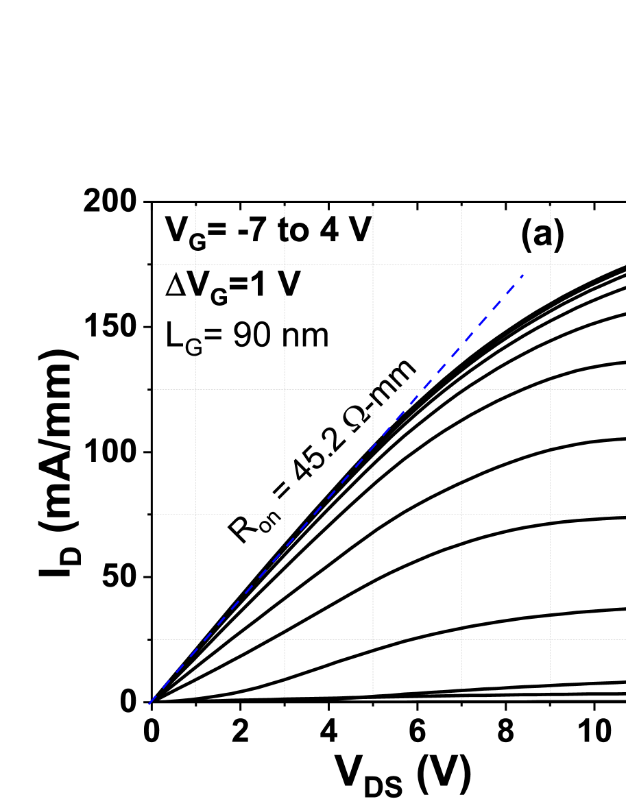
DC ID-VDS output curves shows peak IDS, MAX = 182 mA/mm with 45.2 mm at VDS = 12 V (Fig. 2 (a)). Peak transconductance (gm) was found 37 mS/mm at 10 V drain bias (Fig. 2 (b)). However, only 10 V drain bias was used for transfer curve in order to avoid stressing the device. Higher Ron and lower gm for LG < 100 nm can be attributed to higher channel sheet resistance which increases source resistance (RS) compared to the previous report.
Three terminal off-state breakdown measurement was carried out in air using B1505A power device analyzer. The device was biased at VGS = -15 V which is below VTH. We observed catastrophic breakdown at VDS = 110 V (supplementary material), which corresponds to gate-to-drain breakdown voltage (VBR) of 125 V (VDS- VGS). It results in 1.18 MV/cm average breakdown field (EAVG) for 1.26 m LGD spacing. Lower EAVG can be explained due to air breakdown and lack of external passivation and field management.
Pulsed-IV measurements were carried out using Auriga-AU5 pulse voltage system with low duty cycle to reduce self-heating. No current collapse was observed and pulsed current is higher than DC at high VDS (Fig. 3 (a)) for both gate and drain lag measurements. The increased current can be attributed to reduced self heating effect. Absence of current collapse means that there is possibly no traps under gate or in gate-drain access region Vaidya and Singisetti (2021); Saha, Vaidya, and Singisetti (2022). Pulsed ID-VGS transfer curves shows no shift in threshold voltage for high VDG,Q quiescent bias points (Fig. 3 (b)). This suggests that there are possibly no traps under gate or in the access region in the as deposited Al2O3. However, after repeated DC, RF and large signal measurements, we observed current collapse under pulsed measurements (See Supplementary Material). Electrical stressing may have introduced traps either in the oxide/channel or oxide/air interface. An extrinsic passivation may be necessary to reduce this DC-RF dispersion caused by electrical stressing the device.
Small-signal analysis was performed from 100 MHz to 19 GHz using Keysight ENA 5071C Vector Network Analyzer (VNA). A sapphire calibration standard was used to calibrate The VNA by SOLT technique. An isolated open-pad device structure on the same wafer was utilized to de-embed parasitic pad capacitance Koolen, Geelen, and Versleijen (1991). Short circuit current gain (h21), Mason’s unilateral gain (U) and MAG/MSG have been plotted at VDS = 12 V and VGS = 2 V bias points for LG = 90 nm device. After extrapolating to 0 dB, we found current gain cut-off frequency (ft) of 27 GHz. The power gain cut off frequency (fMAX) is 55 GHz (Fig. 4) which extrapolated from 20dB/decade slope from the Masons’ unilateral gain (U). fMAX value reported here is the highest among Ga2O3 FETs. We calculated the expected intrinsic fT using the geometrically calculated gate source capacitance CGS and measured DC gm (See supplemnatary materials). We assumed half of the channel thickness (30 nm) for CGS calculation. We also calculated extrinsic fT by considering RS, RD calculated from channel sheet resistance and contact resistance. These calculations Tasker and Hughes (1989) gave an intrinsic and extrinsic fT of 29 GHz and 25.5 GHz respectively. This calculation gives further credence to the measured fT and fMAX. In our previous report Saha et al. (2023), we found DC-RF dispersion and reduced high frequency gm was the primary cause of reduced fT.
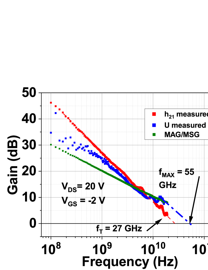
We calculated fMAX based on T gate dimensionTasker and Hughes (1989). Although we do not have any test structure to calculate exact gate resistance (RG), nonetheless our calculation results in fMAX 90 GHz which is higher than our measured data. The discrepancy can be attributed to the higher gate resistance arising from thin metal films and errors in unilateral gain (U) extraction from measured s-parameters. fMAX/fT ratio of 1.8 has been extracted which is similar to our previous reportSaha et al. (2023) and other reports (3 to 5) Zhang et al. (2018a); Kamimura, Nakata, and Higashiwaki (2020); Green et al. (2017) in the literature.
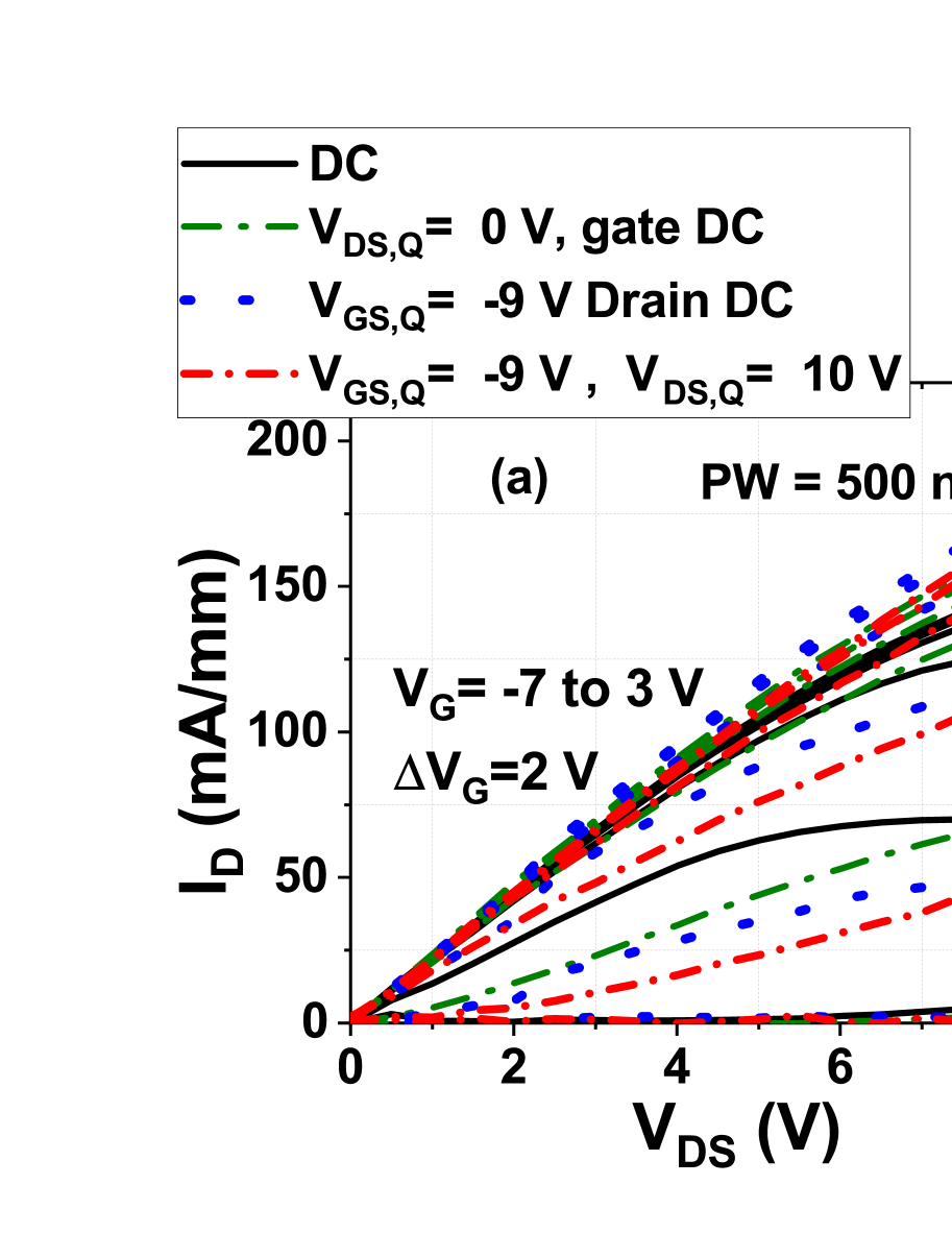
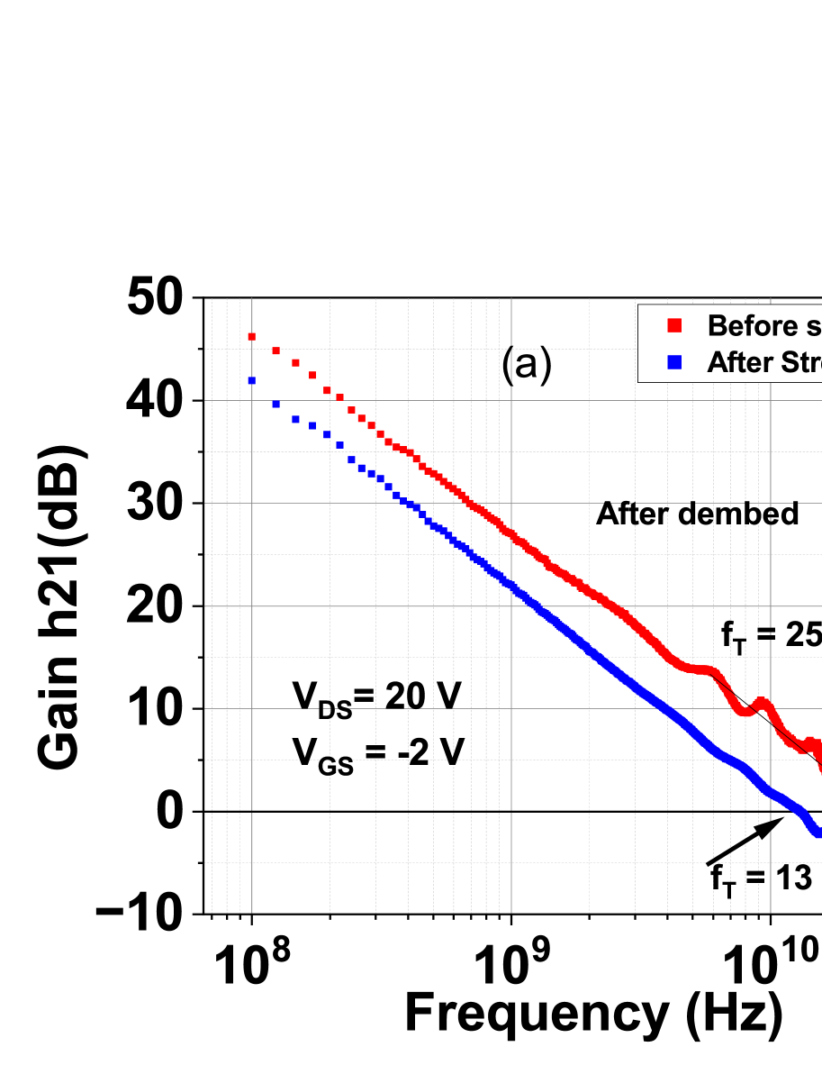
Large signal measurements were attempted on the MOSFETs, however good input matching could not be achieved, thus no large signal data is available. Moreover, we found degradation of both fT and fMAX after repeated DC and large-signal RF measurements. fT dropped to 13 GHz from 25 GHz and fMAX dropped to 12 GHz after DC and large signal measurements (Fig. 5(a) and (b)). Similar characteristics was also observed for all devices; repeated measurements degraded device RF performance significantly (See Supplementary materials). After electrical stressing, the RF gm was lower than DC gm resulting in the fT and fMAX degradation. Pulsed I-V measurements showed current collapse after stressing. Possible trap introduction after repeated DC and large signal measurement may be the primary reason for this. It is noted that these devices did not have the typical external passivation that is used in RF GaN HEMTs. Successful external passivation could mitigate this degradation by electrical stressing. A more careful analysis is necessary to really understand the origin of the degradation of the device.
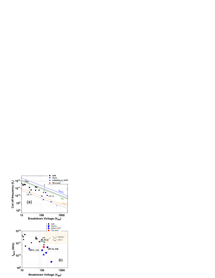
Nevertheless, we calculated Johnson’s Figure of Merit (JFOM) based on the breakdown voltage and fT (un-stressed values). With 125 V breakdown voltage (VBR) and 27 GHz fT, a fT.VBR product of 3.375 GHz.V is achieved, which is comparable to the state-of-art GaN HEMTs (Fig.6(a)). We also bench-marked fMAX and breakdown voltage (VBR) of our device with GaN HEMTs.As seen in Fig. 6(b), this is the only -Ga2O3 device that shows fMAX 55 GHz and VBR > 100 V (Fig. 6(b)) except for a few AlGaN/GaN HEMTs.
In summary, we have demonstrated a 90 nm T gate -Ga2O3 MOSFET with process optimization to eliminate the regrowth interface resistance. We extracted near 55 GHz fMAX, highest among -Ga2O3 devices, with a gate-to-drain breakdown voltage of 125 V. However, degradation of fT and fMAX and current collapse were observed in these un-passivated devices after large signal measurement trials which are possibly caused by trap introduction after repeated DC and RF measurements. Neverthles, the high fMAX is a significant achievement in terms of prospective applications of -Ga2O3 in X band.
SUPPLEMENTARY MATERIAL
See the supplementary material for breakdown analysis, a detailed discussion on RF performance degradation before and after repeated DC, RF measurement. Scatter plot showing degradation of fT, fMAX after different measurements for 5 different devices, pulsed IV measurement for 200 ns pulse width for different bias points showing current collapse after stressing the device.
Acknowledgements.
We acknowledge the support from AFOSR (Air Force Office of Scientific Research) under award FA9550-18-1-0479 (Program Manager: Ali Sayir), from NSF under awards ECCS 2019749, 2231026 from Semiconductor Research Corporation under GRC Task ID 3007.001, and II-VI Foundation Block Gift Program. This work used the electron beam lithography system acquired through NSF MRI award ECCS 1919798. We would like to thank Dr. Andrew Green and Dr. Neil Moser from the Air Force Research Laboratories for their help in large signal measurements.Data Availability Statement
The data that support the findings of this study are available from the corresponding author upon reasonable request.
I REFERENCES
References
- Green et al. (2022) A. J. Green, J. Speck, G. Xing, P. Moens, F. Allerstam, K. Gumaelius, T. Neyer, A. Arias-Purdue, V. Mehrotra, A. Kuramata, et al., “-gallium oxide power electronics,” APL Materials 10, 029201 (2022).
- Green et al. (2016) A. J. Green, K. D. Chabak, E. R. Heller, R. C. Fitch, M. Baldini, A. Fiedler, K. Irmscher, G. Wagner, Z. Galazka, S. E. Tetlak, A. Crespo, K. Leedy, and G. H. Jessen, “3.8-MV/cm breakdown strength of MOVPE-grown Sn-doped -Ga2O3 MOSFETs,” IEEE Electron Device Letters 37, 902–905 (2016).
- Ghosh and Singisetti (2017) K. Ghosh and U. Singisetti, “Ab initio velocity-field curves in monoclinic -Ga2O3,” Journal of Applied Physics 122, 035702 (2017).
- Zeng, Vaidya, and Singisetti (2018) K. Zeng, A. Vaidya, and U. Singisetti, “1.85 kV breakdown voltage in lateral field-plated -Ga2O3,” IEEE Electron Device Letters 39, 1385–1388 (2018).
- Tetzner et al. (2019) K. Tetzner, E. B. Treidel, O. Hilt, A. Popp, S. B. Anooz, G. Wagner, A. Thies, K. Ickert, H. Gargouri, and J. Würfl, “Lateral 1.8 kv -Ga2O3 mosfet with 155 mw/cm 2 power figure of merit,” IEEE Electron Device Letters 40, 1503–1506 (2019).
- Bhattacharyya et al. (2022) A. Bhattacharyya, S. Roy, P. Ranga, C. Peterson, and S. Krishnamoorthy, “High-mobility tri-gate -Ga2O3 MESFETs with a power figure of merit over 0.9 GW/cm2,” IEEE Electron Device Letters 43, 1637–1640 (2022).
- Zhang et al. (2022) J. Zhang, P. Dong, K. Dang, Y. Zhang, Q. Yan, H. Xiang, J. Su, Z. Liu, M. Si, J. Gao, et al., “Ultra-wide bandgap semiconductor ga2o3 power diodes,” Nature communications 13, 3900 (2022).
- Farzana et al. (2021) E. Farzana, F. Alema, W. Y. Ho, A. Mauze, T. Itoh, A. Osinsky, and J. S. Speck, “Vertical -Ga2O3 field plate schottky barrier diode from metal-organic chemical vapor deposition,” Applied Physics Letters 118, 162109 (2021).
- Kalarickal et al. (2021) N. K. Kalarickal, Z. Xia, H.-L. Huang, W. Moore, Y. Liu, M. Brenner, J. Hwang, and S. Rajan, “-(Al0.18Ga0.82)2O3 double heterojunction transistor with average field of 5.5 MV/cm,” IEEE Electron Device Letters 42, 899–902 (2021).
- Saha et al. (2023) C. N. Saha, A. Vaidya, A. F. M. A. U. Bhuiyan, L. Meng, S. Sharma, H. Zhao, and U. Singisetti, “Scaled -Ga2O3 thin channel MOSFET with 5.4 MV/cm average breakdown field and near 50 GHz fMAX,” Applied Physics Letters 122, 182106 (2023).
- Zhang et al. (2018a) Y. Zhang, A. Neal, Z. Xia, C. Joishi, J. M. Johnson, Y. Zheng, S. Bajaj, M. Brenner, D. Dorsey, K. Chabak, G. Jessen, J. Hwang, S. Mou, J. P. Heremans, and S. Rajan, “Demonstration of high mobility and quantum transport in modulation-doped -(AlxGa1-x)2O3 heterostructures,” Applied Physics Letters 112, 173502 (2018a).
- Chabak et al. (2018) K. Chabak, D. Walker, A. Green, A. Crespo, M. Lindquist, K. Leedy, S. Tetlak, R. Gilbert, N. Moser, and G. Jessen, “Sub-micron gallium oxide radio frequency field-effect transistors,” in 2018 IEEE MTT-S International Microwave Workshop Series on Advanced Materials and Processes for RF and THz Applications (IMWS-AMP) (IEEE, 2018) pp. 1–3.
- Xia et al. (2019) Z. Xia, H. Xue, C. Joishi, J. Mcglone, N. K. Kalarickal, S. H. Sohel, M. Brenner, A. Arehart, S. Ringel, S. Lodha, W. Lu, and S. Rajan, “-Ga2O3 delta-doped field-effect transistors with current gain cutoff frequency of 27 GHz,” IEEE Electron Device Letters 40, 1052–1055 (2019).
- Vaidya, Saha, and Singisetti (2021) A. Vaidya, C. N. Saha, and U. Singisetti, “Enhancement mode -(AlxGa1-x)2O3/Ga2O3 heterostructure FET (HFET) with high transconductance and cutoff frequency,” IEEE Electron Device Letters 42, 1444–1447 (2021).
- Saha, Vaidya, and Singisetti (2022) C. N. Saha, A. Vaidya, and U. Singisetti, “Temperature dependent pulsed IV and RF characterization of -(AlxGa1-x)2O3/Ga2O3 hetero-structure FET with ex situ passivation,” Applied Physics Letters 120, 172102 (2022).
- Moser et al. (2020) N. A. Moser, T. Asel, K. J. Liddy, M. Lindquist, N. C. Miller, S. Mou, A. Neal, D. E. Walker, S. Tetlak, K. D. Leedy, et al., “Pulsed power performance of -Ga2O3 mosfets at l-band,” IEEE Electron Device Letters 41, 989–992 (2020).
- Vaidya and Singisetti (2021) A. Vaidya and U. Singisetti, “Temperature-dependent current dispersion study in -Ga2O3 fets using submicrosecond pulsed I-V characteristics,” IEEE Transactions on Electron Devices 68, 3755–3761 (2021).
- Zhang et al. (2018b) Y. Zhang, K. Wei, S. Huang, X. Wang, Y. Zheng, G. Liu, X. Chen, Y. Li, and X. Liu, “High-temperature-recessed millimeter-wave algan/gan hemts with 42.8% power-added-efficiency at 35 ghz,” IEEE Electron Device Letters 39, 727–730 (2018b).
- Ranjan et al. (2014) K. Ranjan, S. Arulkumaran, G. I. Ng, and S. Vicknesh, “High johnson’s figure of merit (8.32 thz· v) in 0.15-m conventional t-gate algan/gan hemts on silicon,” Applied Physics Express 7, 044102 (2014).
- Medjdoub et al. (2013) F. Medjdoub, B. Grimbert, D. Ducatteau, and N. Rolland, “Record combination of power-gain cut-off frequency and three-terminal breakdown voltage for gan-on-silicon devices,” Applied Physics Express 6, 044001 (2013).
- Vaidya et al. (2019) A. Vaidya, J. Sarker, Y. Zhang, L. Lubecki, J. Wallace, J. D. Poplawsky, K. Sasaki, A. Kuramata, A. Goyal, J. A. Gardella, and U. Singisetti, “Structural, band and electrical characterization of -(Al0.19Ga0.81)2O3 films grown by molecular beam epitaxy on sn doped -Ga2O3 substrate,” Journal of Applied Physics 126, 095702 (2019).
- Bhattacharyya et al. (2021) A. Bhattacharyya, P. Ranga, S. Roy, C. Peterson, F. Alema, G. Seryogin, A. Osinsky, and S. Krishnamoorthy, “Multi-kv class -Ga2O3 MESFETs with a lateral figure of merit up to 355 MW/cm2,” IEEE Electron Device Letters 42, 1272–1275 (2021).
- Koolen, Geelen, and Versleijen (1991) M. Koolen, J. Geelen, and M. Versleijen, “An improved de-embedding technique for on-wafer high-frequency characterization,” in Proceedings of the 1991 Bipolar Circuits and Technology Meeting (1991).
- Tasker and Hughes (1989) P. J. Tasker and B. Hughes, IEEE Electron Device Letters 10, 291–293 (1989).
- Kamimura, Nakata, and Higashiwaki (2020) T. Kamimura, Y. Nakata, and M. Higashiwaki, “Delay-time analysis in radio-frequency -Ga2O3 field effect transistors,” Applied Physics Letters 117, 253501 (2020).
- Green et al. (2017) A. J. Green, K. D. Chabak, M. Baldini, N. Moser, R. Gilbert, R. C. Fitch, G. Wagner, Z. Galazka, J. Mccandless, A. Crespo, K. Leedy, and G. H. Jessen, “-Ga2O3 mosfets for radio frequency operation,” IEEE Electron Device Letters 38, 790–793 (2017).
- Kuramata et al. (2016) A. Kuramata, K. Koshi, S. Watanabe, Y. Yamaoka, T. Masui, and S. Yamakoshi, “High-quality -Ga2O3 single crystals grown by edge-defined film-fed growth,” Japanese Journal of Applied Physics 55, 1202A2 (2016).
- Galazka et al. (2016) Z. Galazka, R. Uecker, D. Klimm, K. Irmscher, M. Naumann, M. Pietsch, A. Kwasniewski, R. Bertram, S. Ganschow, and M. Bickermann, “Scaling-up of bulk -Ga2O3single crystals by the czochralski method,” ECS Journal of Solid State Science and Technology 6, Q3007 (2016).
- Tang et al. (2022) W. Tang, Y. Ma, X. Zhang, X. Zhou, L. Zhang, X. Zhang, T. Chen, X. Wei, W. Lin, D. H. Mudiyanselage, H. Fu, and B. Zhang, “High-quality (001) -Ga2O3 homoepitaxial growth by metalorganic chemical vapor deposition enabled by in situ indium surfactant,” Applied Physics Letters 120, 212103 (2022).
- Sasaki et al. (2012) K. Sasaki, A. Kuramata, T. Masui, E. G. Villora, K. Shimamura, and S. Yamakoshi, “Device-quality -Ga2O3 epitaxial films fabricated by ozone molecular beam epitaxy,” Applied Physics Express 5, 035502 (2012).
- Leach et al. (2019) J. Leach, K. Udwary, J. Rumsey, G. Dodson, H. Splawn, and K. Evans, “Halide vapor phase epitaxial growth of -ga2o3 and -ga2o3 films,” APL Materials 7, 022504 (2019).
- Zhou et al. (2016) H. Zhou, S. Alghmadi, M. Si, G. Qiu, and P. D. Ye, “Al2O3/ -Ga2O3(-201) interface improvement through piranha pretreatment and postdeposition annealing,” IEEE Electron Device Letters 37, 1411–1414 (2016).
- Wang et al. (2022) C. Wang, H. Zhou, J. Zhang, W. Mu, J. Wei, Z. Jia, X. Zheng, X. Luo, X. Tao, and Y. Hao, “Hysteresis-free and s-switching of D/E-modes -Ga2O3 hetero-junction FETs with the BV2 /Ron, sp of 0.74/0.28 GW/cm2,” Applied Physics Letters 120, 112101 (2022).
- Islam et al. (2022) A. E. Islam, C. Zhang, K. DeLello, D. A. Muller, K. D. Leedy, S. Ganguli, N. A. Moser, R. Kahler, J. C. Williams, D. M. Dryden, et al., “Defect engineering at the Al2O3 (010)/ -Ga2O3 interface via surface treatments and forming gas post-deposition anneals,” IEEE Transactions on Electron Devices 69, 5656–5663 (2022).
- Meneghesso et al. (2013) G. Meneghesso, M. Meneghini, D. Bisi, I. Rossetto, A. Cester, U. K. Mishra, and E. Zanoni, “Trapping phenomena in AlGaN/GaNHEMTs: A study based on pulsed and transient measurements,” Semiconductor science and technology 28, 074021 (2013).