Current address: ]Departamento de Física, Universidade Estadual de Maringá, 87020-900 Maringá, PR, Brazil
Magnetic field-induced weak-to-strong-link transformation in patterned superconducting films
Abstract
Ubiquitous in most superconducting materials and a common result of nanofabrication processes, weak-links are known for their limiting effects on the transport of electric currents. Still, they are at the root of key features of superconducting technology. By performing quantitative magneto-optical imaging experiments and thermomagnetic model simulations, we correlate the existence of local maxima in the magnetization loops of FIB-patterned Nb films to a magnetic field-induced weak-to-strong-link transformation increasing their critical current. This phenomenon arises from the nanoscale interaction between quantized magnetic flux lines and FIB-induced modifications of the device microstructure. Under an ac drive field, this leads to a rectified vortex motion along the weak-link. The reported tunable effect can be exploited in the development of new superconducting electronic devices, such as flux pumps and valves, to attenuate or amplify the supercurrent through a circuit element, and as a strategy to enhance the critical current in weak-link-bearing devices.
I Introduction
Nanoscale patterning of superconducting films enables the optimization and control of distinct material properties [1, 2, 3, 4, 5, 6, 7, 8, 9]. Moreover, patterning allows exploring different phenomena rising from the rich physics of superconducting weak-links (WLs) [10, 11, 12, 13]. Today, patterned superconducting structures find applications in memories [14, 15, 16, 17], diodes [18, 19], quantum batteries [20], and phase shifters [21, 22], serving as the backbone of superconducting electronics.
Meanwhile, focused-ion beam (FIB) milling is a prominent fabrication technique with nanometric spatial resolution [23, 24, 25]. However, FIB unavoidably introduces defects along the patterned regions, arising from ionic implantation [26, 27, 28], locally increasing vortex pinning in superconductors [3, 8, 29]. Recently, we investigated the effects of a single FIB-milled WL on the properties of prototypical low-critical temperature Nb films, revealing the existence of local maxima in their magnetization loops [30].
Weak-links are also an important challenge in the optimization of large-scale applications of high-temperature superconductors (HTSC) [31, 32]. Particularly, the overall critical current density () of HTSC is affected by an angular-dependent deterioration of along grain boundaries [33, 34], motivating the development of specialized fabrication techniques [35, 36, 37, 38]. Improving critical currents in HTSC and low-critical-temperature materials remains an active research topic [39, 40, 41, 42, 43, 44].
In this study, we investigate magnetic flux penetration and shielding currents in FIB-patterned Nb films containing either a single or four artificial WLs. Our results explain the origin of local maxima in the magnetization loops, revealing a field-induced transformation from a weak-link to a strong-link behavior by the enhancement of across the WL.

II Methods
Three 180-nm-thick Nb films were patterned with a single shallow groove using FIB doses of 0.1, 0.2, and 0.3 nC/µm2 (GF01, GF02, and GF03, respectively). The samples have areas of 3 mm2 (31) in the case of GF01 and 2 mm2 (2.50.8) for the other films. This process creates WLs comprised of thinner Nb regions pervaded by defects arising from Ga+ implantation, as shown in Appendix A. The groove depths range from 4.2 nm to 14.6 nm. Additionally, a 2.5 2.5 mm2 300-nm-thick Nb film labeled GF01+ was deposited and patterned with two perpendicular grooves using a FIB dose of 0.1 nC/µm2 thus exhibiting four distinct WLs in a cross pattern. A pristine film with critical temperature () of 9.0 K is also studied. Sample preparation details are given in Ref. 30. Global dc magnetic responses are obtained in a QD MPMS-5S in the perpendicular geometry. Quantitative magneto-optical imaging (MOI) is used to reveal the local out-of-plane magnetic flux density () and current density () in the films [45, 46].
Furthermore, we employed the thermomagnetic model (TM) to simulate the macroscopic magnetic flux density distribution in the patterned films [47]. For that, the heat diffusion equation
| (1) |
is solved considering Maxwell’s equations and that the superconductor material properties are given by
| (2) |
where is the electric field, the thermal conductivity, the specific heat, the coefficient for heat removal to the substrate, the normal state resistivity, is the film thickness, the sheet current, the critical sheet current, and the flux creep exponent [47]. The simulation parameters used in this work follow Ref. [48].
III Results & discussion
The left panel of Fig. 1(a) schematically represents a superconducting film fully penetrated by flux under a perpendicular magnetic field after zero-field cooling (ZFC) [49, 50]. We observe five dark discontinuity lines, or d-lines, shielding flux more efficiently where changes its direction. The magneto-optical (MO) image at 11.0 Oe demonstrates that flux penetrates from the edges toward the center of the pristine film as is increased. This is manifested by bright, flux-filled regions surrounding the dark, shielded central portion of the sample. At 62.0 Oe, we observe the expected domains for the fully penetrated film. Although the resolution of MOI reveals an apparently continuous flux front, the superconductor is in fact permeated by quantized flux lines, or vortices [51, 52].
In contrast, a groove across the shortest symmetry line of the film creates a WL, defining two apparently disconnected pristine regions (PR). Since the WL has a lower than the PR, needs to bend away from the groove, resulting in the central diamond-shaped domain represented in Fig. 1(b) [53, 54, 55]. In the limiting case when the depicted angle = 45∘, no current is able to flow through the WL, i.e., . MOI for GF01 at 13.9 Oe reveals that the WL is fully penetrated—a consequence of its weaker shielding capacity. At 145.4 Oe, the diamond-shaped domain can be clearly distinguished. Contrary to the representation, MOI shows and a faded dark vertical d-line appears inside the diamond. These effects happen because , meaning that a fraction of is able to flow through the WL. The dark scratches above the diamond-shaped and bottom triangular domains are defects on the MO indicator and do not interfere with the flux penetration into the sample.
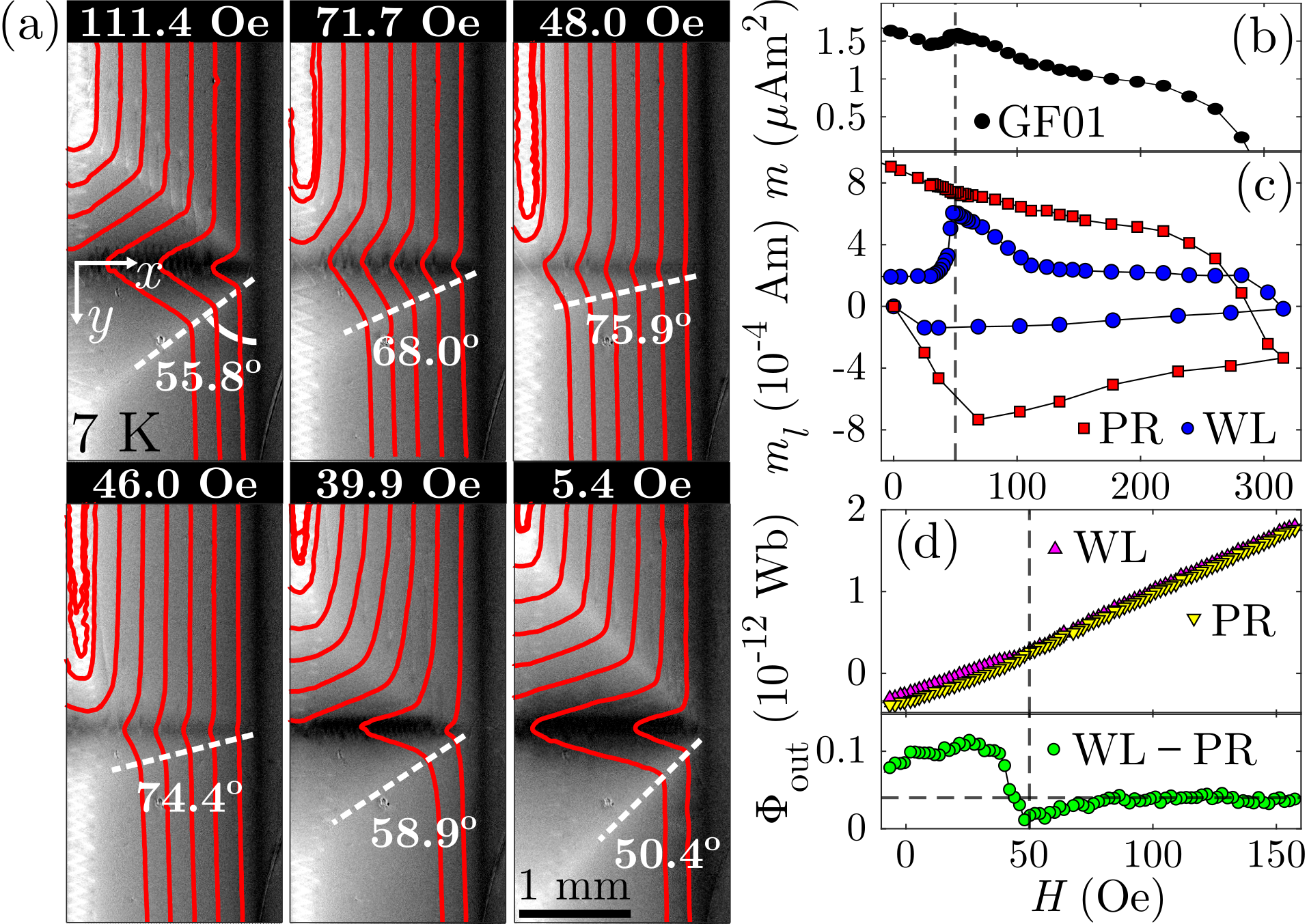
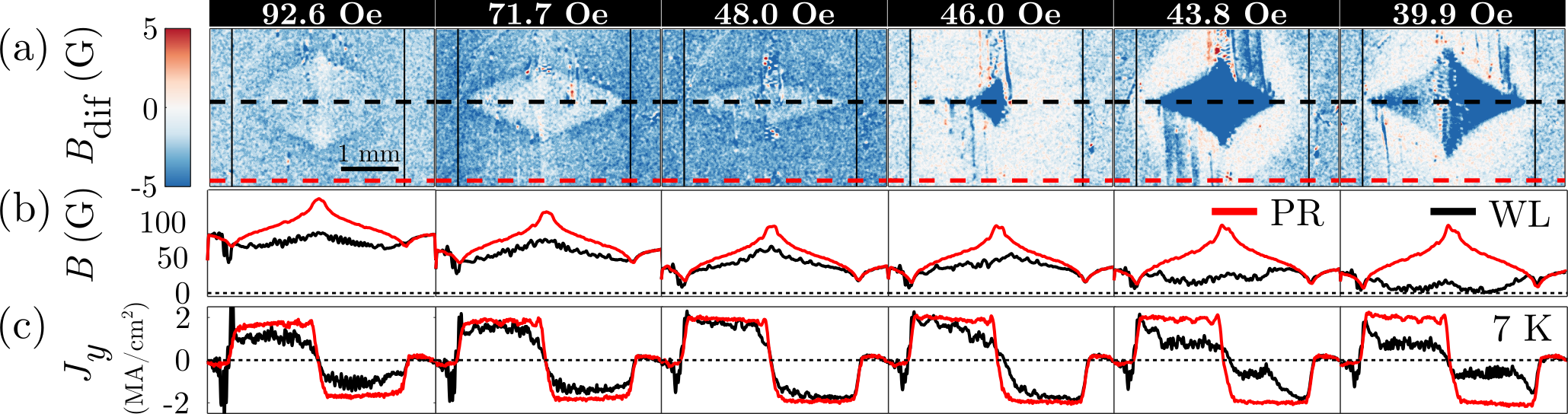
Figure 1(c) shows complete magnetic moment hysteresis loops, , at 7 K for the pristine film and GF02. The pristine behavior matches that expected for a type-II superconductor presenting a flux-dependent critical current density, [56, 57]. In contrast, GF02 exhibits local maxima in the positive and negative decreasing-field branches of . Figure 1(d) reveals the same feature around 50 Oe for GF01 and GF03. Out-of-phase ac magnetic susceptibility () measurements in Fig. 1(e) demonstrate that this effect is sensible to ac excitations. For sufficiently large probe fields, a dip in occurs around the same values at which peaks for GF02. This ac experiment is equivalent to performing a minor loop, as indicated by dashed arrows in Fig. 1(c). Thus, at the upper branch of the loop, while the probe field decreases the total applied field, the sample experiences the same phenomenon giving rise to the peak.
We elect GF01 to illustrate our investigation of what leads to this phenomenon. GF01 contains a 4.2-nm-deep groove with an 800 nm width—see Appendix A. Figure 1(f) shows a series of MO images as is decreased from full penetration. At 140.8 Oe, flux penetration is similar to that of Fig 1(b). The WL now appears in dark contrast, because was reduced from 315.6 Oe, and the WL shows a lower, but positive flux density due to its weaker shielding capability. However, as approaches 50 Oe, the d-lines forming the central diamond-shaped domain move toward the groove—as if they were closing. The image at 50.2 Oe resembles a pristine film, as the diamond shape practically vanishes. If is further reduced, the d-lines move away from the groove, as if they were reopening, reestablishing the diamond-shaped domain, as seen at 25.6 Oe. This analysis demonstrates that MOI is an ideal tool for this study, revealing details of the local flux penetration and current distribution that are hidden in global magnetometry.
The observed d-line movement is associated with an enhancement of the transport properties in the WL. This is demonstrated in Fig. 2(a). As the d-lines close, increases, and changes accordingly—streamlines that initially did not cross the WL become straighter and have a higher density across the WL. This trend is maximized at 48.0 Oe, when the diamond-shaped domain almost fades out. Thus, after the sample is fully penetrated and is reduced to a specific value, the WL behaves as a strong-link, allowing currents to flow through it largely unaffected. At 46.0 Oe and as is further reduced, the d-lines reappear, reestablishing the WL behavior. As is proportional to the height of the curve [58], this notion explains the observed local peak as an increase in the overall due to an increase in .
In Fig. 2(b), we evaluate the magnetic moment of GF01 via MOI as , where is per unit length at a position , is the image pixel size, is the film width, is the sheet current flowing perpendicular to the WL, and is the film thickness [59, 60]. The results reproduce those in Fig. 1(c). Figure 2 also presents quantitative results obtained along the four color-matched regions in Fig. 1(d). In Fig. 2(c), we average over the WL (blue) and on a selected portion of the PR (red), confirming that the peak in manifests an effect tied to the WL. Moreover, we gauge the flux behavior just outside the sample, . Figure 2(d) shows that, as is reduced, is everywhere higher just beside the WL (pink) than beside the PR (yellow) for equal areas. However, as the d-lines are closing, decreases close to the WL while it is unaffected beside the PR, lessening the difference between along the two regions (green). This indicates that fewer vortices are able to escape the sample through the WL at these fields. When the d-lines reopen below 50 Oe, is enhanced besides the groove, indicating a large amount of flux is expelled through the edges of the WL. In the ac experiment, if the device is properly field-biased, this implies a rectified vortex motion characterized by the directed flux movement along the WL albeit vortices are subjected to a zero-mean excitation [61, 62, 63, 64, 65].
Figure 3 locally resolves the behavior of and for GF01. Figure 3(a) depicts the differential flux density, , for GF01. It captures the variation due to the variation of (kept around Oe) by subtracting the target MO image by the one taken at the previous field step, i.e. . In the first three images, we visualize the closing of the d-lines by the shrinking of a brighter diamond-shaped inner region. This indicates that decreases less in that region than outside the d-lines. Therefore, flux is pushed toward the WL as the d-lines close. This agrees with the fact that flux is unable to cross d-lines [66]. At 46.0 Oe, a dark-colored region confirms flux is intensely expelled from the WL. At 43.8 Oe, the bright halo centered in the groove reveals that flux is still being pushed away from the inner part of the sample. For 39.9 Oe and further, the flux pushed out of the WL is systematically reduced.
Figure 3(b) shows the evolution of along the WL (in black) and the PR (red). From 92.6 to 48.0 Oe, the black profile decreases less and becomes increasingly similar to the red one, indicating that the flux pushed inward by the d-line movement is partially retained by the WL. This is related to an increased vortex pinning potential in the WL due to its reduced thickness and FIB-induced defects, which act as pinning centers and locally suppress [3, 30]—see Appendix A. The observed relative increase in corroborates the increase in across the WL seen in Fig. 2(c). Starting at 46.0 Oe, trapped flux is vigorously pushed away from the WL and the profiles become distinct again. As is still positive at 46.0 Oe, the maximum in is not related to a net neutral flux in the WL. Here, we argue that the increased vortex pinning in the WL reduces energy dissipation coming from flux line movement, thus increasing within that specific range. A similar behavior exists in HTSC [67, 68, 60, 69, 70, 71, 72]. The fact that the associated d-line movement was not previously observed in YBCO bicrystalline films [53, 73, 74, 72] may be related to the absence of the FIB-added pinning centers and the relatively higher for which the peak occurs in HTSC, rendering -dependent effects less prominent [57].
Figure 3(c) presents an analysis of perpendicular to the WL, . Initially, there is a gradual increase in the current able to cross the WL. At 48.0 Oe, across the WL closely matches that flowing in the PR—as GF01 behaves almost as a pristine film. This trend is reversed when the d-lines reappear and a sharp decrease in is observed beginning in the center of the WL. The increased current density, paired with the higher vortex concentration at the center of the WL results in a repulsive force that eventually overcomes the pinning force, thus relieving the magnetic pressure built up in the WL and inducing a strong-to-weak-link transformation. Hence, for a field-biased grooved sample subjected to ac fields alternates between maxima and minima in intervals dictated by the drive field. Appendix B depicts the behavior of and at several applied fields, corroborating their relationship to the d-line movement.
With the experimental input, we now turn to numerical simulations based on the thermomagnetic model, which allow for the comprehension of subtle distinctions in specimen behavior arising from a -dependent [75, 76, 48]. The simulated Nb sample shares the geometry of GF01, except for the groove width, set to 45 µm to improve computational performance. Notably, the higher density of pinning sites introduced by Ga implantation in the WL is not considered. A reduction of 15% in the zero-field is induced by reducing in the WL, as experimentally observed—see Appendix A and Ref. 30.
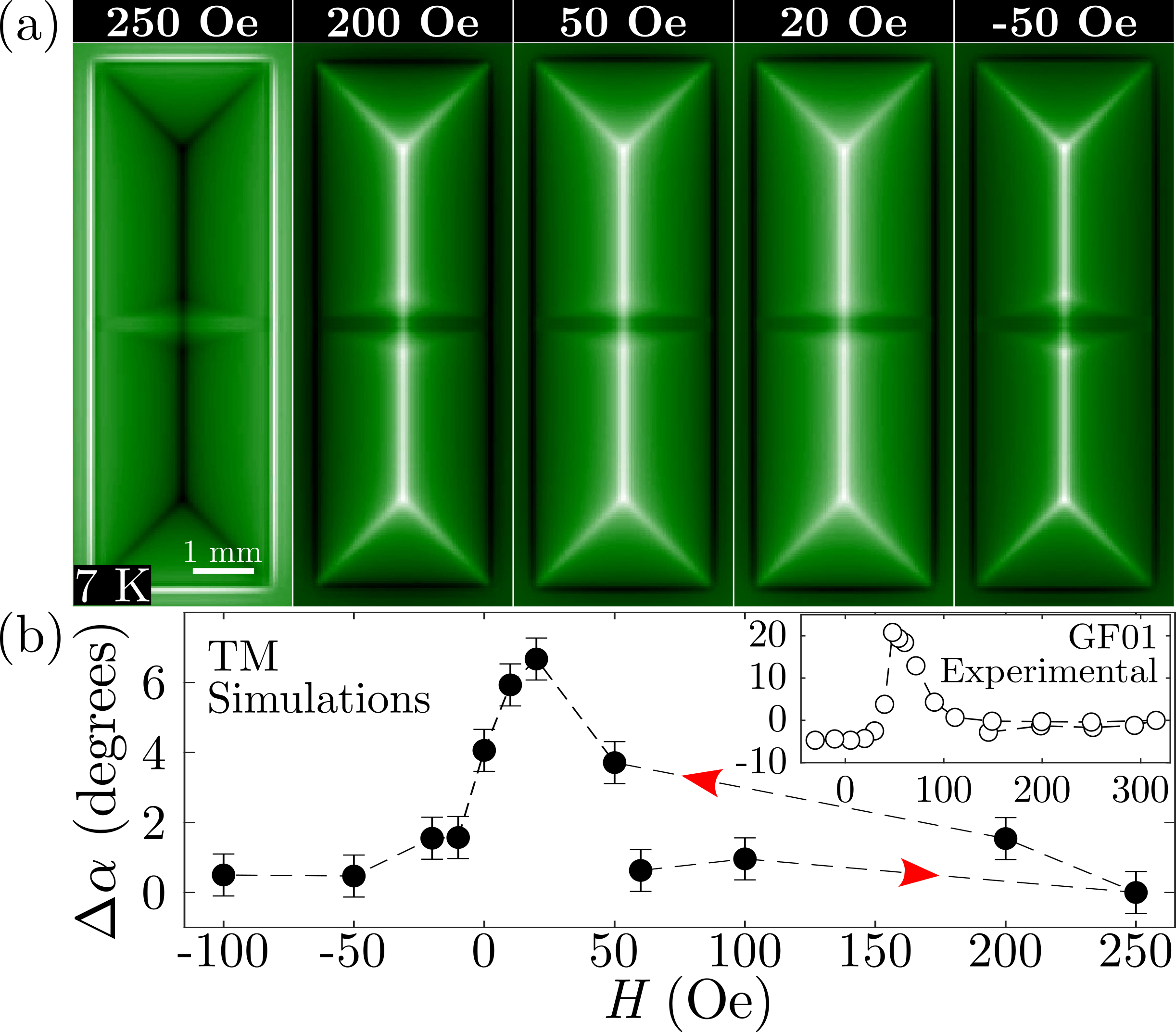
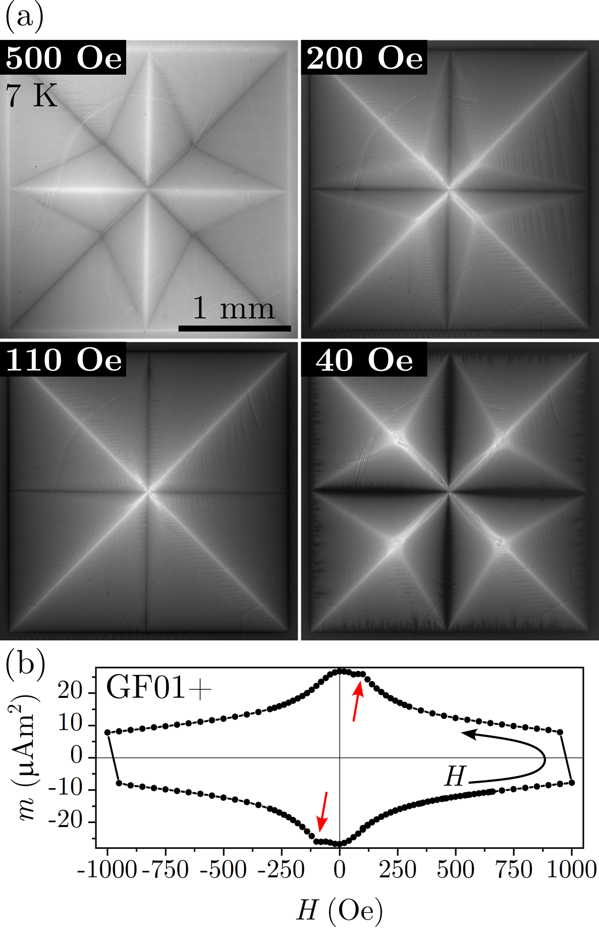
Figure 4 describes the TM results obtained when considering , with [77]. Disorder is introduced by lowering for randomly selected grid points [47]. First, is increased up to 250 Oe after ZFC to 7 K. The resulting flux distribution in Fig. 4(a) qualitatively matches that of GF01 in the full penetration state. Then, is progressively reduced. At 50 Oe, we notice the shrinking of the diamond-shaped domain, which is maximum at 20 Oe. This is quantitatively corroborated by Fig. 4(b), which depicts . The inset of Fig. 4(b) confirms that the simulations reproduce the d-line movement observed experimentally. The lesser closure of the d-lines is likely due to the larger width of the simulated groove. Finally, the d-lines reappear, as demonstrated in Fig. 4(a) at Oe. TM simulations at 7 K indicate a lower threshold of for the occurrence of the reported phenomenon. This is higher than the ratio for GF01 at 7 K due to the different geometry and the irradiation-induced pinning centers. A lower bound for corroborates experimental observations—see Appendix A. Additional simulations, conducted for independent of , did not reproduce the d-line movement, reinforcing the -dependency role in the observed phenomenon.
Finally, Fig. 5(a) presents MO results for GF01+. The weak-links appear in bright contrast at the image captured at the maximum applied field of 500 Oe. Enveloping the WLs, a set of four quadrilateral domains define a remarkable four-pointed star-like pattern [55]. As the field is reduced to 200 Oe, such a pattern systematically fades out, as the d-lines close around the WLs—see Appendix B. At 110 Oe, the observed flux distribution matches that of a pristine square film [58], as all four WLs simultaneously behave as strong-links. This coincides with a local peak in , as revealed by Fig. 5(b). Further reduction will cause the d-lines to reopen, reestablishing the weak-link behavior and the star-like pattern. Therefore, GF01+ behaves completely analogously to GF01 and provides further evidence of the phenomenon reproducibility while revealing it can be scaled up for samples containing multiple WLs.
IV Conclusions
In summary, combining MOI and TM simulations, we demonstrate that the presence of local maxima in the magnetization loops of FIB-patterned Nb films is associated with a field-induced transformation of the sample behavior from weak-to-strong-link. This effect can be tuned by temperature [30] and the amount of defects introduced along the WL. As the transformation is associated with nanoscale interactions between vortices and defects, the phenomenon should also be observed in micro and nanometric devices, more typical size scales for superconducting electronics. Possible applications can take advantage of the vortex rectification and tunable flux escape along the WL in flux pumps or valves. The overall modulation can be explored for constant or periodic signal attenuation or amplification in selected circuit components. Additionally, the targeted inclusion of pinning centers along grain boundaries of weak-link-bearing materials may also lead to the improvement of operating conditions for different superconducting technologies, resulting in effectively higher critical currents for HTSC devices.
Acknowledgements.
This work was partially supported by Coordenação de Aperfeiçoamento de Pessoal de Nível Superior – Brasil (CAPES) – Finance Code 001, the São Paulo Research Foundation (FAPESP, Grant No. 2021/08781-8), and the National Council for Scientific and Technological Development (CNPq, Grants No. 431974/2018-7, No. 316602/2021-3, and No. 309928/2018-4). C. X. acknowledges the support by the National Natural Science Foundation of China (Grants No. 11972298). L. J. was supported by the China Scholarship Council. The authors thank the Laboratory of Structural Characterization (LCE/DEMa/UFSCar) for the EDS and AFM measurements. Research supported by LNNano – Brazilian Nanotechnology National Laboratory (CNPEM/MCTI) during the use of the Device Manufacturing open access facility.Appendix A Morphology, structure, and superconducting properties
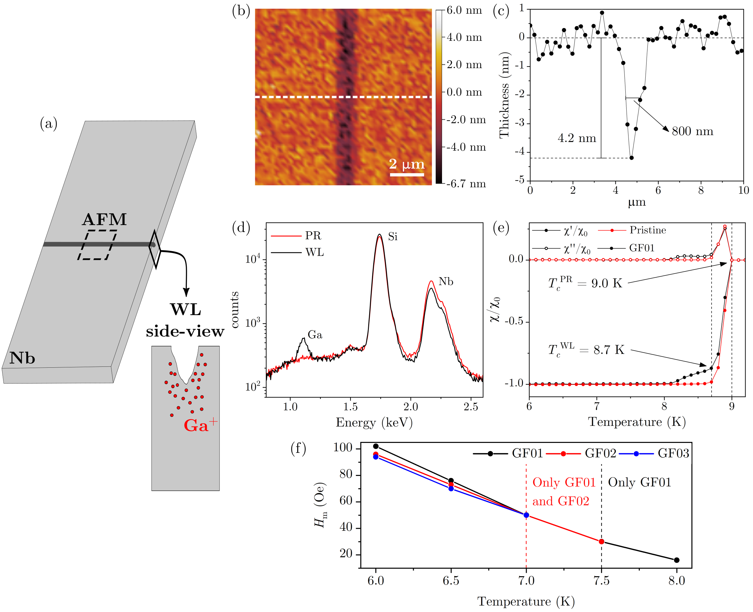
The Nb samples are deposited by magnetron sputtering on a SiO2 substrate, as described in Ref. [30]. The single-WL samples are schematically represented in Fig. 6(a), where the grooved region appears in dark in the center of the film, spanning the whole sample’s width. The lower right corner shows a sketch of the weak-link lateral profile, representing the FIB-milled-induced defects arising from Ga implantation as red circles. SRIM simulations [78] indicate Ga ions penetrate less than 30 nm into the Nb film. As described in Refs. [30, 26, 27], the Ga implantation is an unavoidable consequence of FIB-milling, leading to a suppression of the Nb sample superconducting properties.
Figure 6(b) presents Atomic-Force Microscopy (AFM) results for GF01 centered around the WL, confirming the presence of the groove. The AFM measurements were conducted on a Digital Instruments Nanoscope V. The thickness values are presented with respect to the average height of the Nb film, which highlights the groove depth. In Fig. 6(c), a thickness profile is plotted centered along the white dashed line in panel (b). The points are averaged for a 110 µm2 area. The profile reveals a maximum groove depth of 4.2 nm for GF01, as well as an 800 nm width at half depth.
Figure 6(d) confirms the Ga implantation inside the WL. This is accomplished by performing an Energy Dispersive X-ray Spectrometry (EDS), conducted using a Philips XL-30 FEG Scanning Electron Microscope. We take EDS spectra of GF02 of both the pristine region (PR) and the WL, which are shown in red and black, respectively. For the PR, EDS reveals characteristic K\textalpha emission peaks for Si (due to the substrate) and Nb. However, when the WL is gauged, an additional emission line due to the presence of Ga is observed.
Figure 6(e) demonstrates the deterioration of the superconducting properties in the WL due to the milling process. It shows the temperature-dependency of both in-phase () and out-of-phase () AC-susceptibility components for GF01, in black, and the pristine sample, in red. The results were obtained on a SQUID-based Quantum Design MPMS-5S magnetometer and the curves for each sample are normalized by their respective Meissner state plateau, . A 100 Hz probe AC-magnetic field with 0.5 Oe amplitude was used in the measurements. The results show a single sharp superconducting transition at = 9.0 K for the pristine sample. However, a two-step transition is observed for GF01, revealing a second transition, related to the WL, at = 8.7 K [30].
Figure 6(f) depicts the variation of the field at which the magnetization peak is observed () as a function of temperature for GF01, GF02, and GF03. The values are obtained from curves measured at different temperatures. It shows that, as temperature increases, the samples exposed to lower FIB doses still present a maximum in , whereas those exposed to higher doses do not. This is associated with a reduction of the ratio between the zero-field current able to flow through the WL in comparison to the PR, . As the films patterned by a higher FIB dose present a larger concentration of defects at the WL, they experience a further reduction of . Therefore, as the emergence of the magnetization peak depends on , GF03 will not present the reported phenomenon at lower temperatures when compared to GF02, which, in turn, does not do so at lower temperatures than GF01.
Appendix B Magnetic flux penetration
![[Uncaptioned image]](/html/2305.04262/assets/VideoGF01-snapshot.png)
The magnetic flux and shielding current behavior in GF01 at 7 K as the applied magnetic field is increased and decreased. The dark and red profiles highlight the behavior along the WL and the PR, respectively.
Video B shows MOI of GF01 at 47 different applied magnetic fields, both while is increased after ZFC to 7 K and while it is decreased from a maximum applied value of 315.6 Oe. Besides the MO images, and profiles are shown for each of the presented values. The profiles are evaluated on the PR (in red) and along the WL (in black), as indicated by color-matched arrows beside the MO images. A green profile is also presented and it is obtained by subtracting across the WL from across the PR. Noticeably, there is a scratch on the MO indicator film beside the left side of the groove. This creates rather visual discontinuities on the left side of the black profiles but does not interfere with the interpretation of the behavior inside the WL. The video corroborates the discussion presented in the main text by showing the gradual increase in across the WL as is reduced accompanied by the relative increase in in the same region. This happens as the central discontinuity lines, visible in the MO images, close toward the groove.
Video B shows the flux penetration patterns into sample GF01+ at 7 K after zero-field cooling as is increased up to 500 Oe and subsequently decreased back to 0 Oe. The video corroborates the simultaneous d-line movement along all four weak-links as the applied field is reduced, as discussed in the main text.
![[Uncaptioned image]](/html/2305.04262/assets/VideoGF01cross-snapshot.png)
Magnetic flux penetration into GF01 at 7 K as the applied magnetic field is increased and decreased.
References
- Harada et al. [1996] K. Harada, O. Kamimura, H. Kasai, T. Matsuda, A. Tonomura, and V. V. Moshchalkov, Direct observation of vortex dynamics in superconducting films with regular arrays of defects, Science 274, 1167 (1996).
- Silhanek et al. [2003] A. V. Silhanek, L. Van Look, S. Raedts, R. Jonckheere, and V. V. Moshchalkov, Guided vortex motion in superconductors with a square antidot array, Phys. Rev. B 68, 214504 (2003).
- Dobrovolskiy et al. [2012] O. V. Dobrovolskiy, E. Begun, M. Huth, and V. A. Shklovskij, Electrical transport and pinning properties of Nb thin films patterned with focused ion beam-milled washboard nanostructures, New J. Phys. 14, 113027 (2012).
- Shaw et al. [2012] G. Shaw, P. Mandal, B. Bag, S. Banerjee, T. Tamegai, and H. Suderow, Properties of nanopatterned pins generated in a superconductor with FIB, Appl. Surf. Sci. 258, 4199 (2012).
- Wang et al. [2013] Y. L. Wang, M. L. Latimer, Z. L. Xiao, R. Divan, L. E. Ocola, G. W. Crabtree, and W. K. Kwok, Enhancing the critical current of a superconducting film in a wide range of magnetic fields with a conformal array of nanoscale holes, Phys. Rev. B 87, 220501 (2013).
- Dobrovolskiy [2017] O. V. Dobrovolskiy, Abrikosov fluxonics in washboard nanolandscapes, Physica C 533, 80 (2017).
- Kalcheim et al. [2017] Y. Kalcheim, E. Katzir, F. Zeides, N. Katz, Y. Paltiel, and O. Millo, Dynamic control of the vortex pinning potential in a superconductor using current injection through nanoscale patterns, Nano Lett. 17, 2934 (2017).
- Dobrovolskiy et al. [2017] O. V. Dobrovolskiy, V. A. Shklovskij, M. Hanefeld, M. Zörb, L. Köhs, and M. Huth, Pinning effects on flux flow instability in epitaxial Nb thin films, Supercond. Sci. Technol. 30, 085002 (2017).
- Colauto et al. [2020] F. Colauto, M. Motta, and W. A. Ortiz, Controlling magnetic flux penetration in low- superconducting films and hybrids, Supercond. Sci. Technol. 34, 013002 (2020).
- Likharev [1979] K. K. Likharev, Superconducting weak links, Rev. Mod. Phys. 51, 101 (1979).
- Moshchalkov et al. [2010] V. Moshchalkov, R. Woerdenweber, and W. Lang, eds., Nanoscience and engineering in superconductivity (Springer Berlin, Heidelberg, 2010).
- Fornieri et al. [2019] A. Fornieri, A. M. Whiticar, F. Setiawan, E. Portolés, A. C. Drachmann, A. Keselman, S. Gronin, C. Thomas, T. Wang, R. Kallaher, et al., Evidence of topological superconductivity in planar Josephson junctions, Nature 569, 89 (2019).
- Holzman and Ivry [2019] I. Holzman and Y. Ivry, Superconducting nanowires for single-photon detection: Progress, challenges, and opportunities, Adv. Quantum Technol. 2, 1800058 (2019).
- Murphy et al. [2017] A. Murphy, D. V. Averin, and A. Bezryadin, Nanoscale superconducting memory based on the kinetic inductance of asymmetric nanowire loops, New J. Phys. 19, 063015 (2017).
- Chen et al. [2020] L. Chen et al., Miniaturization of the superconducting memory cell via a three-dimensional Nb nano-superconducting quantum interference device, ACS Nano 14, 11002 (2020).
- Ilin et al. [2021] E. Ilin, X. Song, I. Burkova, A. Silge, Z. Guo, K. Ilin, and A. Bezryadin, Supercurrent-controlled kinetic inductance superconducting memory element, Appl. Phys. Lett. 118, 112603 (2021).
- Chaves et al. [2023] D. A. D. Chaves, L. Nulens, H. Dausy, B. Raes, D. Yue, W. A. Ortiz, M. Motta, M. J. Van Bael, and J. Van de Vondel, Nanobridge SQUIDs as multilevel memory elements, Phys. Rev. Appl. 19, 034091 (2023).
- Lyu et al. [2021] Y.-Y. Lyu et al., Superconducting diode effect via conformal-mapped nanoholes, Nat. Commun. 12, 1 (2021).
- Golod and Krasnov [2022] T. Golod and V. M. Krasnov, Demonstration of a superconducting diode-with-memory, operational at zero magnetic field with switchable nonreciprocity, Nat. Commun. 13, 3658 (2022).
- Strambini et al. [2020] E. Strambini et al., A Josephson phase battery, Nat. Nanotechnol. 15, 656 (2020).
- Yamashita et al. [2020] T. Yamashita, S. Kim, H. Kato, W. Qiu, K. Semba, A. Fujimaki, and H. Terai, phase shifter based on NbN-based ferromagnetic Josephson junction on a silicon substrate, Sci. Rep. 10, 1 (2020).
- Golod et al. [2021] T. Golod, R. A. Hovhannisyan, O. M. Kapran, V. V. Dremov, V. S. Stolyarov, and V. M. Krasnov, Reconfigurable Josephson phase shifter, Nano Lett. 21, 5240 (2021).
- Volkert and Minor [2007] C. A. Volkert and A. M. Minor, Focused ion beam microscopy and micromachining, MRS Bull. 32, 389 (2007).
- Wyss et al. [2022] M. Wyss, K. Bagani, D. Jetter, E. Marchiori, A. Vervelaki, B. Gross, J. Ridderbos, S. Gliga, C. Schönenberger, and M. Poggio, Magnetic, thermal, and topographic imaging with a nanometer-scale SQUID-on-lever scanning probe, Phys. Rev. Appl. 17, 034002 (2022).
- Sigloch et al. [2022] F. Sigloch, S. Sangiao, P. Orús, and J. M. de Teresa, Direct-write of tungsten-carbide nanoSQUIDs based on focused ion beam induced deposition, Nanoscale Adv. 4, 4628 (2022).
- Datesman et al. [2005] A. M. Datesman, J. C. Schultz, T. W. Cecil, C. M. Lyons, and A. W. Lichtenberger, Gallium ion implantation into niobium thin films using a focused-ion beam, IEEE Trans. Appl. Supercond. 15, 3524 (2005).
- De Leo et al. [2016] N. De Leo, M. Fretto, V. Lacquaniti, C. Cassiago, L. D’Ortenzi, L. Boarino, and S. Maggi, Thickness modulated niobium nanoconstrictions by focused ion beam and anodization, IEEE Trans. Appl. Supercond. 26, 1 (2016).
- Singh et al. [2018] M. Singh, R. Chaujar, S. Husale, S. Grover, A. P. Shah, M. M. Deshmukh, A. Gupta, V. N. Singh, V. N. Ojha, D. K. Aswal, and R. K. Rakshit, Influence of fabrication processes on transport properties of superconducting niobium nitride nanowires, Current Science 114, 1443 (2018).
- Aichner et al. [2019] B. Aichner, B. Müller, M. Karrer, V. R. Misko, F. Limberger, K. L. Mletschnig, M. Dosmailov, J. D. Pedarnig, F. Nori, R. Kleiner, D. Koelle, and W. Lang, Ultradense tailored vortex pinning arrays in superconducting YBa2Cu3O7-δ thin films created by focused He ion beam irradiation for fluxonics applications, ACS Appl. Nano Mater. 2, 5108 (2019).
- Valerio-Cuadros et al. [2021] M. I. Valerio-Cuadros, D. A. D. Chaves, F. Colauto, A. A. M. Oliveira, A. M. H. Andrade, T. H. Johansen, W. A. Ortiz, and M. Motta, Superconducting properties and electron scattering mechanisms in a Nb film with a single weak-link excavated by focused ion beam, Materials 14, 7274 (2021).
- Larbalestier et al. [2001] D. Larbalestier, A. Gurevich, D. M. Feldmann, and A. Polyanskii, High- superconducting materials for electric power applications, Nature 414, 368 (2001).
- Foltyn et al. [2007] S. R. Foltyn, L. Civale, J. L. MacManus-Driscoll, Q. X. Jia, B. Maiorov, H. Wang, and M. Maley, Materials science challenges for high-temperature superconducting wire, Nat. Mater. 6, 631 (2007).
- Hilgenkamp and Mannhart [2002] H. Hilgenkamp and J. Mannhart, Grain boundaries in high- superconductors, Rev. Mod. Phys. 74, 485 (2002).
- Graser et al. [2010] S. Graser, P. J. Hirschfeld, T. Kopp, R. Gutser, B. M. Andersen, and J. Mannhart, How grain boundaries limit supercurrents in high-temperature superconductors, Nat. Phys. 6, 609 (2010).
- Reade et al. [1992] R. P. Reade, P. Berdahl, R. E. Russo, and S. M. Garrison, Laser deposition of biaxially textured yttria‐stabilized zirconia buffer layers on polycrystalline metallic alloys for high critical current Y‐Ba‐Cu‐O thin films, Appl. Phys. Lett. 61, 2231 (1992).
- Iijima et al. [1993] Y. Iijima, K. Onabe, N. Futaki, N. Tanabe, N. Sadakata, O. Kohno, and Y. Ikeno, Structural and transport properties of biaxially aligned YBa2Cu3O7-x films on polycrystalline Ni‐based alloy with ion‐beam‐modified buffer layers, J. Appl. Phys. 74, 1905 (1993).
- Wu et al. [1995] X. D. Wu, S. R. Foltyn, P. N. Arendt, W. R. Blumenthal, I. H. Campbell, J. D. Cotton, J. Y. Coulter, W. L. Hults, M. P. Maley, H. F. Safar, and J. L. Smith, Properties of YBa2Cu3O7-δ thick films on flexible buffered metallic substrates, Appl. Phys. Lett. 67, 2397 (1995).
- Goyal et al. [1996] A. Goyal, D. P. Norton, J. D. Budai, M. Paranthaman, E. D. Specht, D. M. Kroeger, D. K. Christen, Q. He, B. Saffian, F. A. List, D. F. Lee, P. M. Martin, C. E. Klabunde, E. Hartfield, and V. K. Sikka, High critical current density superconducting tapes by epitaxial deposition of YBa2Cu3Ox thick films on biaxially textured metals, Appl. Phys. Lett. 69, 1795 (1996).
- Díez-Sierra et al. [2020] J. Díez-Sierra et al., High critical current density and enhanced pinning in superconducting films of YBa2Cu3O7-δ nanocomposites with embedded BaZrO3, BaHfO3, BaTiO3, and SrZrO3 nanocrystals, ACS Appl. Nano Mater. 3, 5542 (2020).
- Ahmad et al. [2021] I. Ahmad, S. Sarangi, and P. Sarun, Enhanced critical current density and flux pinning of anthracene doped magnesium diboride superconductor, J. Alloys Compd. 884, 160999 (2021).
- Rocci et al. [2020] M. Rocci, D. Suri, A. Kamra, G. Vilela, Y. Takamura, N. M. Nemes, J. L. Martinez, M. G. Hernandez, and J. S. Moodera, Large enhancement of critical current in superconducting devices by gate voltage, Nano Lett. 21, 216 (2020).
- Caffer et al. [2021] A. M. Caffer, D. A. D. Chaves, A. L. Pessoa, C. L. Carvalho, W. A. Ortiz, R. Zadorosny, and M. Motta, Optimum heat treatment to enhance the weak-link response of Y123 nanowires prepared by solution blow spinning, Supercond. Sci. Technol. 34, 025009 (2021).
- Algarni et al. [2021] R. Algarni, M. A. Almessiere, Y. Slimani, E. Hannachi, and F. B. Azzouz, Enhanced critical current density and flux pinning traits with Dy2O3 nanoparticles added to YBa2Cu3O7-d superconductor, J. Alloys Compd. 852, 157019 (2021).
- Chaves et al. [2021] D. A. D. Chaves, I. M. de Araújo, D. Carmo, F. Colauto, A. A. M. Oliveira, A. M. H. Andrade, T. H. Johansen, A. V. Silhanek, W. A. Ortiz, and M. Motta, Enhancing the effective critical current density in a Nb superconducting thin film by cooling in an inhomogeneous magnetic field, Appl. Phys. Lett. 119, 022602 (2021).
- Shaw et al. [2018] G. Shaw, J. Brisbois, L. B. G. L. Pinheiro, J. Müller, S. Blanco Alvarez, T. Devillers, N. M. Dempsey, J. E. Scheerder, J. Van de Vondel, S. Melinte, P. Vanderbemden, M. Motta, W. A. Ortiz, K. Hasselbach, R. B. G. Kramer, and A. V. Silhanek, Quantitative magneto-optical investigation of superconductor/ferromagnet hybrid structures, Rev. Sci. Instrum. 89, 023705 (2018).
- Meltzer et al. [2017] A. Y. Meltzer, E. Levin, and E. Zeldov, Direct reconstruction of two-dimensional currents in thin films from magnetic-field measurements, Phys. Rev. Applied 8, 064030 (2017).
- Vestgården et al. [2011] J. I. Vestgården, D. V. Shantsev, Y. M. Galperin, and T. H. Johansen, Dynamics and morphology of dendritic flux avalanches in superconducting films, Phys. Rev. B 84, 054537 (2011).
- Jiang et al. [2020] L. Jiang, C. Xue, L. Burger, B. Vanderheyden, A. V. Silhanek, and Y.-H. Zhou, Selective triggering of magnetic flux avalanches by an edge indentation, Phys. Rev. B 101, 224505 (2020).
- Schuster et al. [1994a] T. Schuster, M. V. Indenbom, M. R. Koblischka, H. Kuhn, and H. Kronmüller, Observation of current-discontinuity lines in type-II superconductors, Phys. Rev. B 49, 3443 (1994a).
- Schuster et al. [1995] T. Schuster, H. Kuhn, and M. V. Indenbom, Discontinuity lines in rectangular superconductors with intrinsic and extrinsic anisotropies, Phys. Rev. B 52, 15621 (1995).
- Mints and Rakhmanov [1981] R. G. Mints and A. L. Rakhmanov, Critical state stability in type-II superconductors and superconducting-normal-metal composites, Rev. Mod. Phys. 53, 551 (1981).
- Blatter et al. [1994] G. Blatter, M. V. Feigel’man, V. B. Geshkenbein, A. I. Larkin, and V. M. Vinokur, Vortices in high-temperature superconductors, Rev. Mod. Phys. 66, 1125 (1994).
- Polyanskii et al. [1996] A. A. Polyanskii, A. Gurevich, A. E. Pashitski, N. F. Heinig, R. D. Redwing, J. E. Nordman, and D. C. Larbalestier, Magneto-optical study of flux penetration and critical current densities in [001] tilt YBa2Cu3O7-δ thin-film bicrystals, Phys. Rev. B 53, 8687 (1996).
- Johansen et al. [2019] T. H. Johansen, F. Colauto, A. M. H. de Andrade, A. A. M. Oliveira, and W. A. Ortiz, Transparency of planar interfaces in superconductors: a critical-state analysis, IEEE Trans. Appl. Supercond. 29, 1 (2019).
- Colauto et al. [2021] F. Colauto, D. Carmo, A. M. H. Andrade, A. A. M. Oliveira, W. A. Ortiz, Y. M. Galperin, and T. H. Johansen, Measurement of critical current flow and connectivity in systems of joined square superconducting plates, Physica C 589, 1353931 (2021).
- Kim et al. [1963] Y. B. Kim, C. F. Hempstead, and A. R. Strnad, Magnetization and critical supercurrents, Phys. Rev. 129, 528 (1963).
- Shantsev et al. [2000] D. V. Shantsev, Y. M. Galperin, and T. H. Johansen, Thin superconducting disk with field-dependent critical current: Magnetization and ac susceptibilities, Phys. Rev. B 61, 9699 (2000).
- Johansen and Bratsberg [1995] T. H. Johansen and H. Bratsberg, Critical‐state magnetization of type‐II superconductors in rectangular slab and cylinder geometries, J. Appl. Phys. 77, 3945 (1995).
- Brandt and Indenbom [1993] E. H. Brandt and M. Indenbom, Type-II-superconductor strip with current in a perpendicular magnetic field, Phys. Rev. B 48, 12893 (1993).
- Shantsev et al. [1999] D. V. Shantsev, M. R. Koblischka, Y. M. Galperin, T. H. Johansen, L. Půst, and M. Jirsa, Central peak position in magnetization loops of high- superconductors, Phys. Rev. Lett. 82, 2947 (1999).
- Wambaugh et al. [1999] J. F. Wambaugh, C. Reichhardt, C. J. Olson, F. Marchesoni, and F. Nori, Superconducting fluxon pumps and lenses, Phys. Rev. Lett. 83, 5106 (1999).
- Olson et al. [2001] C. J. Olson, C. Reichhardt, B. Jankó, and F. Nori, Collective interaction-driven ratchet for transporting flux quanta, Phys. Rev. Lett. 87, 177002 (2001).
- Togawa et al. [2005] Y. Togawa, K. Harada, T. Akashi, H. Kasai, T. Matsuda, F. Nori, A. Maeda, and A. Tonomura, Direct observation of rectified motion of vortices in a niobium superconductor, Phys. Rev. Lett. 95, 087002 (2005).
- de Souza Silva et al. [2006a] C. C. de Souza Silva, J. Van de Vondel, B. Y. Zhu, M. Morelle, and V. V. Moshchalkov, Vortex ratchet effects in films with a periodic array of antidots, Phys. Rev. B 73, 014507 (2006a).
- de Souza Silva et al. [2006b] C. C. de Souza Silva, J. Van de Vondel, M. Morelle, and V. V. Moshchalkov, Controlled multiple reversals of a ratchet effect, Nature 440, 651 (2006b).
- Schuster et al. [1994b] T. Schuster, M. V. Indenbom, M. R. Koblischka, H. Kuhn, and H. Kronmüller, Observation of current-discontinuity lines in type-II superconductors, Phys. Rev. B 49, 3443 (1994b).
- Evetts and Glowacki [1988] J. E. Evetts and B. A. Glowacki, Relation of critical current irreversibility to trapped flux and microstructure in polycrystalline YBa2Cu3O7, Cryogenics 28, 641 (1988).
- Dimos et al. [1990] D. Dimos, P. Chaudhari, and J. Mannhart, Superconducting transport properties of grain boundaries in YBa2Cu3O7 bicrystals, Phys. Rev. B 41, 4038 (1990).
- Hogg et al. [2001] M. J. Hogg, F. Kahlmann, Z. H. Barber, and J. E. Evetts, Angular hysteresis in the critical current of YBa2Cu3O7 low-angle grain boundaries, Supercond. Sci. Technol. 14, 647 (2001).
- Thompson et al. [2004] J. R. Thompson, H. J. Kim, C. Cantoni, D. K. Christen, R. Feenstra, and D. T. Verebelyi, Self-organized current transport through low-angle grain boundaries in YBa2Cu3O7-δ thin films studied magnetometrically, Phys. Rev. B 69, 104509 (2004).
- Palau et al. [2004] A. Palau, T. Puig, X. Obradors, E. Pardo, C. Navau, A. Sanchez, A. Usoskin, H. C. Freyhardt, L. Fernández, B. Holzapfel, and R. Feenstra, Simultaneous inductive determination of grain and intergrain critical current densities of YBa2Cu3O7-x coated conductors, Appl. Phys. Lett. 84, 230 (2004).
- Palau et al. [2007] A. Palau, T. Puig, X. Obradors, and C. Jooss, Simultaneous determination of grain and grain-boundary critical currents in YBa2Cu3O7-coated conductors by magnetic measurements, Phys. Rev. B 75, 054517 (2007).
- Guth et al. [2004] K. Guth, V. Born, and C. Jooss, Inhomogeneous current distribution in wide high-temperature superconducting small-angle grain boundaries, Eur. Phys. J. B 42, 239 (2004).
- Born et al. [2004] V. Born, K. Guth, H. C. Freyhardt, and C. Jooss, Self-enhanced flux penetration into small angle grain boundaries in YBCO thin films, Supercond. Sci. Technol. 17, 380 (2004).
- Jing et al. [2016] Z. Jing, H. Yong, and Y. Zhou, Influences of non-uniformities and anisotropies on the flux avalanche behaviors of type-II superconducting films, Supercond. Sci. Technol. 29, 105001 (2016).
- Jing et al. [2017] Z. Jing, H. Yong, and Y. Zhou, Numerical simulation on the flux avalanche behaviors of microstructured superconducting thin films, J. Appl. Phys. 121, 023902 (2017).
- Kim et al. [1962] Y. B. Kim, C. F. Hempstead, and A. R. Strnad, Critical persistent currents in hard superconductors, Phys. Rev. Lett. 9, 306 (1962).
- Ziegler and Biersack [1985] J. F. Ziegler and J. P. Biersack, The stopping and range of ions in matter, in Treatise on Heavy-Ion Science: Volume 6: Astrophysics, Chemistry, and Condensed Matter, edited by D. A. Bromley (Springer US, Boston, MA, 1985) pp. 93–129.