MilliKelvin microwave impedance microscopy in a dry dilution refrigerator
Abstract
Microwave impedance microscopy (MIM) is a near-field imaging technique that has been used to visualize the local conductivity of materials with nanoscale resolution across the GHz regime. In recent years, MIM has shown great promise for the investigation of topological states of matter, correlated electronic states and emergent phenomena in quantum materials. To explore these low-energy phenomena, many of which are only detectable in the milliKelvin regime, we have developed a novel low-temperature MIM incorporated into a dilution refrigerator. This setup, which consists of a tuning-fork-based atomic force microscope with microwave reflectometry capabilities, is capable of reaching temperatures down to during imaging and magnetic fields up to . To test the performance of this microscope, we demonstrate microwave imaging of the conductivity contrast between graphite and silicon dioxide at cryogenic temperatures and discuss the resolution and noise observed in these results. We extend this methodology to visualize edge conduction in Dirac semimetal cadmium arsenide in the quantum Hall regime.
I Introduction
Microwave imaging techniques have been developing rapidly over the past several decades, which involve transmitting MHz to GHz microwave signals to sample surface through sharp-ended probes, and collecting the microwave response. To date there are several implementations of the scanning microwave microscope, such as sharp tips in coaxial resonators, microwave resonators on quartz tuning forks, and probes with impedance matching networks Takeuchi et al. (1997); Lee, Lee, and Anlage (2005); de Graaf et al. (2013); De Graaf, Danilov, and Kubatkin (2015); Geaney et al. (2019); Lai et al. (2007). In this article we focus on the specific implementation of microwave impedance microscopy (MIM), which has shown capacities to probe the local conductivity and permittivity of quantum materials with nanoscale spatial resolutionRosner and van der Weide (2002); Lai et al. (2007); Huber et al. (2010); Lai et al. (2011a, b); Kundhikanjana et al. (2013); Ma et al. (2015a, b); Liu et al. (2015); Seabron et al. (2016); Chu et al. (2020); Barber, Ma, and Shen (2022). This enables direct visualization of the microscopic nature of electronic states, including the real-space disorder landscape, multi-domain behavior, high-Tc superconductors, or the presence of topological modes that propagate along the sample boundariesTakeuchi et al. (1997); Lee and Anlage (2003); Lee, Lee, and Anlage (2005); Tai et al. (2014); De Graaf, Danilov, and Kubatkin (2015); Geaney et al. (2019). By coupling microwaves with a wavelength of 1- to a sharp metallic probe and collecting the reflected signal, MIM characterizes the complex admittance between the tip and the sample without the requirement for the sample to be conductive, which is less restrictive than other electronic imaging techniquesEriksson et al. (1996); Döring, Eng, and Kehr (2016); Lu et al. (2017); McGilly et al. (2019); Rosenberger et al. (2020). As demonstrated in recent experiments, MIM can provide insight into the real-space nature of correlated states and topological states in two-dimensional heterostructuresLai et al. (2008, 2010); Ma et al. (2015c); Wu et al. (2018); Allen et al. (2019); Chu et al. (2020); Barber, Ma, and Shen (2022). However, many of these states are characterized by low energy scales and are therefore most robust at millikelvin temperatures, motivating the development of cryogenic MIM instrumentation. Thus far, most state-of-the-art near-field microwave imaging has been performed in 1.5-Kundhikanjana et al. (2011) or He-3 cryostats, which can reach of a minimum temperature of 300- de Graaf et al. (2013); Allen et al. (2019).
Here we report on the construction of a novel milliKelvin MIM, which will support spatially-resolved detection of quantum electronic states at ultra-low temperatures. This setup consists of scanning probe microscope with tuning-fork-based height feedback integrated into a dry dilution refrigerator. A sharp metallic probe driven by an AC signal at microwave frequency is coupled to the tuning fork and scanned over the sample. Using reflectometry, MIM detects the sample’s response to high frequency electromagnetic fields emanating from the probe.
To demonstrate the measurement capabilities of this setup, we present MIM images of the conductivity contrast between graphite and SiO2 down to temperatures of 70 mK. Finally, we also demonstrate microwave imaging of edge states in \ceCd3As2 thin films in the quantum Hall regime at the base temperature.
II Experimental Setup
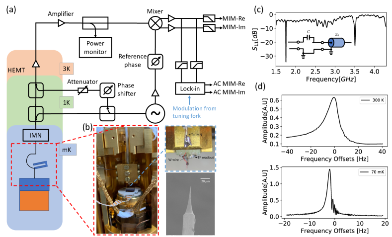
This setup consists of an custom-designed tuning fork based atomic force microscope (AFM) integrated into a Leiden Cryogenics CF-CS110 dilution refrigerator. The microscope housing is in thermal equilibrium with the mixing chamber plate on the cold-insertable probe, which is loaded into a dilution refrigerator, as shown schematically in Figure 1(a). Figure 1(b) shows the design of the microscope head, which houses an etched tungsten wire mounted onto to the end of one prong of a tuning fork (TF) mechanical resonator (blue box) Khan et al. (2012). The oscillation amplitude of the TF is monitored for continuous height feedback, which enables tapping-mode topographic imagingEdwards et al. (1997). Below the tip holder, the sample stage is mounted on a stack of CuBe piezoelectric scanners (Attocube AN-Sxyz100) and the positioners (ANPx(z)100), which control fine xyz scanning (up to below ) and coarse positioning ( below ), respectively.
On the MIM circuitry side, GHz signals are generated by an analog signal generator, and one split branch of the signal is coupled to the tip via an impedance matching network (IMN) Pozar (2011), which is responsible for minimizing the reflected signal [inset in Figure 1(c)] Cui, Ma, and Shen (2016). Unless otherwise mentioned, measurements in the article are done with source power, and the power reaching the tip is . A plot of the reflected microwave power of an example IMN is shown in Figure 1(c), showing the first resonance at . The reflected signal from the tip passes through two directional couplers mounted on the probe-still plate () to cancel out the residual reflected power.
The signal from the sample is then amplified by a cryogenic amplifier (Cosmic Microwave Technology CITCRYO1-12) mounted on the stage, after which the signal propagates out of the probe and gets further amplified and demodulated at room temperature, as shown in Figure 1(a).
During the tip approach procedure, active height feedback can be performed by monitoring either the TF oscillation amplitude or the MIM signal. Here we use a Nanonis SC5 controller to excite and track the TF oscillation and control the fine scanners during imaging Cui, Ma, and Shen (2016).Figure 1(d) displays a measurement of the oscillation amplitude of the tuning fork as a function of excitation frequency, showing the resonance peak near 32.768 kHz. The Q-factor of the resonance is around 500 - 2000 at room temperature (upper panel), while at base temperature it can easily reach 10,000-100,000 (lower panel).
The main technical challenge of microwave imaging in a dry dilution fridge is the emergence of new noise sources, which impact both spatial resolution and the signal-to-noise of the microwave reflectometry measurements. There are two main sources of increased noise: (1) mechanical pulse tube vibrations, which are associated with the cooling mechanism of the dilution fridge, place limits on the lateral spatial resolution and add noise to the measured MIM signal, and (2) the high Q factor of the tuning fork at mK temperatures leads to fluctuations in the tip-sample distance, which also couples with the pulse tube vibration. Our fridge is equipped with a pulse tube cryocooler operating at Wang and Gifford (2002); Chijioke and Lawall (2010) generating vibrations that amplitude modulate the tuning fork oscillation, and consequently also modulate the GHz MIM signal. To mitigate these vibrations, we physically decoupled the pulse tube motion from the microscope by unscrewing the rotary valve from the fridge and putting isolation foam in between Li et al. (2005), while the high-pressure helium lines connected to the compressor are wrapped with acoustic pipe lagging. On the other hand, the high Q factor can be reduced by further breaking the symmetry of the two prongs, and two methods we have been using include adding extra glue during the tip-gluing process, and balancing the strain from the tip to the TF.
We found that performing AC-mode MIM imaging, described below, largely eliminates background oscillations in the images that arise from pulse tube vibrations. In AC height-modulated imaging mode, a low frequency lock-in amplifier (SR830) is added to the output of the GHz frequency mixer to demodulate the reflected MIM signal at the tuning fork resonance frequency (32 kHz), after which low-pass filters can be used to attenuate noise Cui, Ma, and Shen (2016). We note that because the GHz MIM signal (from the tip) is amplitude-modulated by both the tuning fork oscillation at 32 kHz and the pulse tube vibration, there are multiple side-bands around the measurement frequency. Therefore, voltage preamplifiers with band-pass filters between 10-30 kHz (SR560, 6 dB/oct) are added to the output of the GHz mixer to both filter out the DC-MIM signal which would overload the lock-in amplifier, amplify the signal amplitude and reduce the out-of-band noise, after which the MIM signal is fed into the SR830 lock-in amplifier for demodulation. During this step, the lock-in amplifier multiplies the MIM input signal with a TF reference signal (provided by the measured piezo current from the tuning fork, after amplification by a commercial low-noise charge amplifier) to extract the in-phase components. Both the filters inside SR830 and the additional low-pass filters (SR560, 1 Hz low-pass) added to the output of the lock-in are chosen to eliminate noise at the pulse tube vibration frequency.
III Results and Discussion
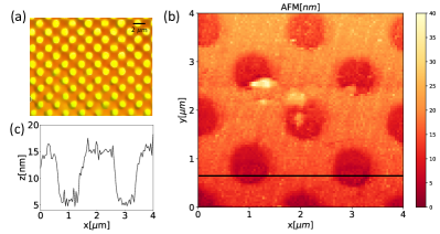
We characterized the low temperature performance of the AFM on a sample consisting of an array of etched holes patterned on a Si wafer, as depicted in the optical image in Figure 2(a). Cryogenic AFM measurements are used to visualize the topographic profile of a 5 m 5 m scan region at , as depicted in Figure 2(b). Figure 2(c) shows a cross-sectional cut of this AFM image, whose position is marked by the black line, revealing a noise level of roughly . To more carefully assess the magnitude of the z-noise during AFM scanning, we performed 96 96-pixel noise scans over a 1 nm 1 nm area, such that the spatial profile is irrelevant. Root mean square (RMS) roughness was calculated using Gwyddion after line fitting, which gives z-noise levels in the range of 1.8 - 2.2 nm. Furthermore, upon careful inspection of Figure 2(b), we noticed that a tilted stripe pattern appears as a background modulation in the AFM image. By taking a Fourier transform of this data, we found that the stripe pattern has a frequency of , which coincides with the frequency of the pulse tube.
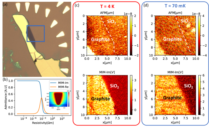
Next, to demonstrate our combined AFM and MIM imaging capabilities at low temperatures, we measured the spatial contrast of the MIM response across the boundary between graphite and SiO2 at 70 mK. Figure 3(a) shows an optical image of the graphite sample, which has terraces of varying thicknesses: the purple region is and the bright yellow region is 15-.
In Figure 3, panels (c) and (d) display AFM and MIM images of the graphite/SiO2 interface measured at 4K and , respectively. In both sets of AFM images, the 3/ step height in graphite is clearly visible, while the graphite/SiO2 boundary only shows a faint contour, as the z-movement of the scanner to compensate for fluctuations in the tip-sample distance dominates over the boundary. Meanwhile, we observe a sharp contrast in the MIM signal across the graphite/SiO2 boundary due to the different conductivities of the two materials, as predicted by the response curves in Figure 3(b). To explain the experimental observations, one can model the tip-sample interaction for this system using finite element analysisWu et al. (2018). In the numerical simulation, the tip is defined to be and the bottom of the \ceSiO2 is set at , the ground. The side of the sample is electrically floating. For a sample with a scalar conductivity, the simulation can be used to calculate the MIM response curves as a function of sample resistivity, which should be expected to have a response curve similar to the lump-circuit model defined for MIM imagingBarber, Ma, and Shen (2022); Wang et al. (2023). For a better discussion of lump-circuit model, readers can refer to the supplementary information. At a measurement frequency of 1.8 GHz, the imaginary part of the MIM response should monotonically decrease with the sample resistivity, saturating when the resistivity is higher than (insulating limit) or lower than (conductive limit), as shown in Figure 3(b). A cross-sectional profile of the penetration of the tip potential into the sample is provided in the inset. Based on our observation in the imaging, we estimate the MIM spatial resolution to be below , constrained by the apex geometry of the etched tungsten tip and mechanical noise from pulse tube vibrations.
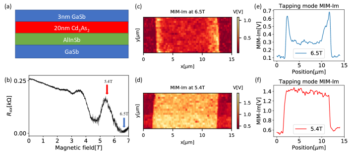
We also apply this methodology to visualize edge states at the boundaries of thin film cadmium arsenide (\ceCd3As2), a novel three-dimensional Dirac semi-metal, in the quantum Hall regimeSankar et al. (2015); Schumann et al. (2016). A cross-sectional schematic of the epitaxially-grown hetero-structure is shown in Figure4 (a), where the film thickness is Goyal et al. (2018); Lygo et al. (2023). The \ceCd3As2 device is lithographically patterned and etched into strips of width 10-15 m, which are electrically grounded. Transport measurements were performed to characterize the magnetic field behavior of the sample, which reveal dips in the longitudinal resistance at around and , as shown in Figure 4(b). These minima should correspond to the emergence of quantum Hall plateausGuo et al. (2022).
To shed light on the real-space conductivity profile of \ceCd3As2 in the quantum Hall regime and monitor its evolution across the topological phase transition between plateaus, MIM measurements were performed at a series of magnetic fields at a base temperature of 90 mK. Microwave imaging reveals a sharp enhancement of the reflected MIM signal at the boundaries of the sample in the quantum Hall insulator state, which rapidly decays into the bulk of the sample, as shown in Figure 4(c). Meanwhile, we observed a spatially-uniform conductivity at the transition between quantum Hall plateaus when the longitudinal resistance deviates from zero at B = 5.4 T (Figure 4(d)). The variation of the MIM signal between different lines comes both from the noise in the MIM signal and spatial inhomogeneities in the sample.
To more clearly compare the spatial dependence of the MIM signal in these two regimes, in Figure 4(e-f) we plot the cross-sectional profiles of the MIM response across the sample extracted from panels (c) and (d), respectively. These low temperature microwave images reveal sharply enhanced edge conduction that encloses an insulating interior in the quantum Hall regime, which is consistent with the results of transport measurements performed on this system in prior experimental studies.
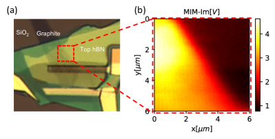
We note that one way to improve signal quality is to use “floating” AC-mode MIM, where imaging is performed with the tip retracted a fixed distance (60-) above the sample surface. At this distance, the AFM channel will not be modulated due to the topography feedback, but the MIM tip can still interact with the sample via the electromagnetic fields in the vicinity of the tip (when operated in the near-field regime). Because periodic oscillations in the tip-sample distance at the tuning fork resonance are decoupled from the surface roughness of the sample, noise in the MIM response can be dramatically reduced in floating mode. Figure 5 shows the results of a floating mode MIM scan performed at and T= , with the tip lifted above an hBN-covered graphite layer. The tip apex is around , which is reflected in the spatial profile of the MIM signal change across the boundary between the graphite flake and hBN. In this case, the signal-to-noise ratio is even better than that observed in tapping mode MIM images (Figure 3(c-d), which is especially useful for fixed-location MIM measurements. However, this advantage comes at the expense of signal size, as the tip is further away from the sample than for tapping mode. The varying MIM signal in the graphite region is due to the fact that during a floating scan the tip is hovering at a fixed absolute z-position, while the sample has a surface tilt, which means the tip-sample distance is varying in the whole frame. We estimate the distance to be around in the upper-left corner and in the lower-right corner.
The choice of tip-sample distance for floating-mode measurements is a compromise between maximizing signal sensitivity and minimizing the risk of a tip crash due to vertical fluctuations in the tip-sample distance, which arise from pulse tube vibrations and are aggravated by the large Q factor of the tuning fork at mK temperatures. For larger scan windows or rougher sample surfaces, the tip may need to be retracted further. We expect the sensitivity of floating mode to be around at input power, and in our case the noise is mostly due to vertical modulations of the tip-sample distanceLai et al. (2008).
IV Conclusion and outlook
In summary, we report on the development of a microwave impedance microscope that operates at temperatures down to . This is achieved by incorporating a TF-based AFM with near-field GHz imaging capabilities into a dry dilution refrigerator.
Pushing the limits of MIM into new low temperature regimes should enable local sensing of quantum phenomena that only exist at low energy scales, including certain topological states of matter, domain wall physics at phase transitions, quantum states arising from geometric confinement in mesoscopic devices, and correlated states in two-dimensional materials and van der Waals heterostructures. Because this instrumentation is equipped with combined transport and imaging capabilities, it can also illuminate the correspondence between macroscopic transport behavior and the underlying microscopic nature of electronic states, including the real-space disorder landscape or presence of edge modes.
During the preparation of this manuscript, we became aware of an article on a related topicJiang et al. (2023). We are using the same tuning-fork based MIM circuitry, and in this manuscript we focus our efforts on mitigating the relevant AFM and MIM noise caused by the fluctuation in tip-sample distance. The z-resolution of AFM in the reference is in the order of 0.1-0.3 nm, while in our case it’s 3-20nm. The MIM sensitivity in the reference is mainly limited by the MIM setup, while our MIM sensitivity is constrained by the vertical tip-sample variation.
supplementary material
The supplementary material includes more information on the analysis of the pulse tube vibration frequency, a description of the lumped element model of MIM, and the determination of the MIM spatial resolution.
Acknowledgements.
We thank Alex Lygo and Susanne Stemmer for providing cadmium arsenide devices for these experiments, Yongtao Cui for inspiring discussions, and Evan Cobb for helping develop some of the MIM circuitry. We gratefully acknowledge funding support from the UC Office of the President, specifically the UC Laboratory Fees Research Program (award LFR-20-653926), the AFOSR Young Investigator Program (award FA9550-20-1-0035) and the AFOSR/ARO MURI Program (award FA9550-22-1-0270). This work was performed, in part, at the San Diego Nanotechnology Infrastructure (SDNI) of UCSD, a member of the National Nanotechnology Coordinated Infrastructure, which is supported by the National Science Foundation (Grant ECCS-2025752).Data Availability
The data that support the findings of this study are available from the corresponding author upon reasonable request.
References
- Takeuchi et al. (1997) I. Takeuchi, T. Wei, F. Duewer, Y. K. Yoo, X.-D. Xiang, V. Talyansky, S. P. Pai, G. J. Chen, and T. Venkatesan, “Low temperature scanning-tip microwave near-field microscopy of films,” Applied Physics Letters 71, 2026–2028 (1997).
- Lee, Lee, and Anlage (2005) S.-C. Lee, S.-Y. Lee, and S. M. Anlage, “Microwave nonlinearities of an isolated long bicrystal grain boundary,” Physical Review B 72, 024527 (2005).
- de Graaf et al. (2013) S. E. de Graaf, A. V. Danilov, A. Adamyan, and S. E. Kubatkin, “A near-field scanning microwave microscope based on a superconducting resonator for low power measurements,” Review of Scientific Instruments 84, 023706 (2013).
- De Graaf, Danilov, and Kubatkin (2015) S. De Graaf, A. Danilov, and S. Kubatkin, “Coherent interaction with two-level fluctuators using near field scanning microwave microscopy,” Scientific reports 5, 17176 (2015).
- Geaney et al. (2019) S. Geaney, D. Cox, T. Hönigl-Decrinis, R. Shaikhaidarov, S. Kubatkin, T. Lindström, A. Danilov, and S. de Graaf, “Near-field scanning microwave microscopy in the single photon regime,” Scientific reports 9, 12539 (2019).
- Lai et al. (2007) K. Lai, M. Ji, N. Leindecker, M. Kelly, and Z. Shen, “Atomic-force-microscope-compatible near-field scanning microwave microscope with separated excitation and sensing probes,” Review of scientific instruments 78, 063702 (2007).
- Rosner and van der Weide (2002) B. T. Rosner and D. W. van der Weide, “High-frequency near-field microscopy,” Review of Scientific Instruments 73, 2505–2525 (2002).
- Huber et al. (2010) H. P. Huber, M. Moertelmaier, T. M. Wallis, C.-J. Chiang, M. Hochleitner, A. Imtiaz, Y. J. Oh, K. Schilcher, M. Dieudonne, J. Smoliner, P. Hinterdorfer, S. J. Rosner, H. Tanbakuchi, P. Kabos, and F. Kienberger, “Calibrated nanoscale capacitance measurements using a scanning microwave microscope.” The Review of scientific instruments 81 11, 113701 (2010).
- Lai et al. (2011a) K. Lai, W. Kundhikanjana, M. A. Kelly, and Z. xun Shen, “Nanoscale microwave microscopy using shielded cantilever probes,” Applied Nanoscience 1, 13–18 (2011a).
- Lai et al. (2011b) K. Lai, W. Kundhikanjana, M. A. Kelly, Z.-X. Shen, J. Shabani, and M. Shayegan, “Imaging of coulomb-driven quantum hall edge states,” Phys. Rev. Lett. 107, 176809 (2011b).
- Kundhikanjana et al. (2013) W. Kundhikanjana, Y. Yang, Q. Tanga, K. Zhang, K. Lai, Y. Ma, M. Kelly, X. Li, and Z. Shen, “Unexpected surface implanted layer in static random access memory devices observed by microwave impedance microscope,” Semiconductor science and technology 28, 025010 (2013).
- Ma et al. (2015a) E. Y. Ma, M. R. Calvo, J. Wang, B. Lian, M. Mühlbauer, C. Brüne, Y.-T. Cui, K. Lai, W. Kundhikanjana, Y. Yang, et al., “Unexpected edge conduction in mercury telluride quantum wells under broken time-reversal symmetry,” Nature communications 6, 7252 (2015a).
- Ma et al. (2015b) E. Y. Ma, Y.-T. Cui, K. Ueda, S. Tang, K. Chen, N. Tamura, P. M. Wu, J. Fujioka, Y. Tokura, and Z.-X. Shen, “Mobile metallic domain walls in an all-in-all-out magnetic insulator,” Science 350, 538–541 (2015b).
- Liu et al. (2015) Y. Liu, C. Tan, H. Chou, A. Nayak, D. Wu, R. Ghosh, H.-Y. Chang, Y. Hao, X. Wang, J.-S. Kim, et al., “Thermal oxidation of nanosheets adhered on / substrates,” Nano letters 15, 4979–4984 (2015).
- Seabron et al. (2016) E. Seabron, S. MacLaren, X. Xie, S. V. Rotkin, J. A. Rogers, and W. L. Wilson, “Scanning probe microwave reflectivity of aligned single-walled carbon nanotubes: Imaging of electronic structure and quantum behavior at the nanoscale,” ACS nano 10, 360–368 (2016).
- Chu et al. (2020) Z. Chu, E. C. Regan, X. Ma, D. Wang, Z. Xu, M. I. B. Utama, K. Yumigeta, M. Blei, K. Watanabe, T. Taniguchi, S. Tongay, F. Wang, and K. Lai, “Nanoscale conductivity imaging of correlated electronic states in Moir’e superlattices,” Physical Review Letters 125, 186803 (2020).
- Barber, Ma, and Shen (2022) M. E. Barber, E. Y. Ma, and Z.-X. Shen, “Microwave impedance microscopy and its application to quantum materials,” Nature Reviews Physics 4, 61–74 (2022).
- Lee and Anlage (2003) S.-C. Lee and S. M. Anlage, “Spatially-resolved nonlinearity measurements of bicrystal grain boundaries,” Applied Physics Letters 82, 1893–1895 (2003).
- Tai et al. (2014) T. Tai, B. G. Ghamsari, T. R. Bieler, T. Tan, X. X. Xi, and S. M. Anlage, “Near-field microwave magnetic nanoscopy of superconducting radio frequency cavity materials,” Applied Physics Letters 104, 232603 (2014).
- Eriksson et al. (1996) M. Eriksson, R. Beck, M. Topinka, J. Katine, R. Westervelt, K. Campman, and A. Gossard, “Cryogenic scanning probe characterization of semiconductor nanostructures,” Applied Physics Letters 69, 671–673 (1996).
- Döring, Eng, and Kehr (2016) J. Döring, L. M. Eng, and S. C. Kehr, “Low-temperature piezoresponse force microscopy on barium titanate,” Journal of Applied Physics 120, 084103 (2016).
- Lu et al. (2017) C.-I. Lu, C. J. Butler, J.-K. Huang, Y.-H. Chu, H.-H. Yang, C.-M. Wei, L.-J. Li, and M.-T. Lin, “Moiré-related in-gap states in a twisted /graphite heterojunction,” npj 2D Materials and Applications 1, 24 (2017).
- McGilly et al. (2019) L. McGilly, A. Kerelsky, N. Finney, K. Shapovalov, E.-M. Shih, A. Ghiotto, Y. Zeng, S. Moore, W. Wu, Y. Bai, et al., “Seeing moir’e superlattices,” arXiv preprint arXiv:1912.06629 (2019).
- Rosenberger et al. (2020) M. R. Rosenberger, H.-J. Chuang, M. Phillips, V. P. Oleshko, K. M. McCreary, S. V. Sivaram, C. S. Hellberg, and B. T. Jonker, “Twist angle-dependent atomic reconstruction and moiré patterns in transition metal dichalcogenide heterostructures,” ACS nano 14, 4550–4558 (2020).
- Lai et al. (2008) K. Lai, W. Kundhikanjana, M. Kelly, and Z. X. Shen, “Modeling and characterization of a cantilever-based near-field scanning microwave impedance microscope,” Review of Scientific Instruments 79, 063703 (2008), https://doi.org/10.1063/1.2949109 .
- Lai et al. (2010) K. Lai, M. Nakamura, W. Kundhikanjana, M. Kawasaki, Y. Tokura, M. A. Kelly, and Z.-X. Shen, “Mesoscopic percolating resistance network in a strained manganite thin film,” Science 329, 190–193 (2010).
- Ma et al. (2015c) E. Y. Ma, B. Bryant, Y. Tokunaga, G. Aeppli, Y. Tokura, and Z.-X. Shen, “Charge-order domain walls with enhanced conductivity in a layered manganite,” Nature Communications 6, 7595 (2015c).
- Wu et al. (2018) X. Wu, Z. Hao, D. Wu, L. Zheng, Z. Jiang, V. Ganesan, Y. Wang, and K. Lai, “Quantitative measurements of nanoscale permittivity and conductivity using tuning-fork-based microwave impedance microscopy,” Review of Scientific Instruments 89, 043704 (2018).
- Allen et al. (2019) M. Allen, Y. Cui, E. Yue Ma, M. Mogi, M. Kawamura, I. C. Fulga, D. Goldhaber-Gordon, Y. Tokura, and Z.-X. Shen, “Visualization of an axion insulating state at the transition between 2 chiral quantum anomalous hall states,” Proceedings of the National Academy of Sciences 116, 14511–14515 (2019).
- Kundhikanjana et al. (2011) W. Kundhikanjana, K. Lai, M. A. Kelly, and Z.-X. Shen, “Cryogenic microwave imaging of metal–insulator transition in doped silicon,” Review of Scientific Instruments 82, 033705 (2011).
- Khan et al. (2012) Y. Khan, H. Al-Falih, Y. Zhang, T. K. Ng, and B. S. Ooi, “Two-step controllable electrochemical etching of tungsten scanning probe microscopy tips,” Review of Scientific Instruments 83, 063708 (2012).
- Edwards et al. (1997) H. Edwards, L. Taylor, W. Duncan, and A. J. Melmed, “Fast, high-resolution atomic force microscopy using a quartz tuning fork as actuator and sensor,” Journal of Applied Physics 82, 980–984 (1997).
- Pozar (2011) D. M. Pozar, Microwave engineering (John wiley & sons, 2011).
- Cui, Ma, and Shen (2016) Y.-T. Cui, E. Y. Ma, and Z.-X. Shen, “Quartz tuning fork based microwave impedance microscopy,” Review of Scientific Instruments 87, 063711 (2016).
- Wang and Gifford (2002) C. Wang and P. Gifford, “Development of 4 k pulse tube cryorefrigerators at cryomech,” in AIP conference proceedings, Vol. 613 (American Institute of Physics, 2002) pp. 641–648.
- Chijioke and Lawall (2010) A. Chijioke and J. Lawall, “Vibration spectrum of a pulse-tube cryostat from 1hz to 20khz,” Cryogenics 50, 266–270 (2010).
- Li et al. (2005) R. Li, Y. Ikushima, T. Koyama, T. Tomaru, T. Suzuki, T. Haruyama, T. Shintomi, and A. Yamamoto, “Vibration-free pulse tube cryocooler system for gravitational wave detectors, part ii: cooling performance and vibration,” in Cryocoolers 13 (Springer, 2005) pp. 703–710.
- Wang et al. (2023) T. Wang, C. Wu, M. Mogi, M. Kawamura, Y. Tokura, Z.-X. Shen, Y.-Z. You, and M. T. Allen, “Theory of the microwave impedance microscopy of chern insulators,” arXiv preprint arXiv:2304.09227 (2023).
- Sankar et al. (2015) R. Sankar, M. Neupane, S.-Y. Xu, C. Butler, I. Zeljkovic, I. Panneer Muthuselvam, F.-T. Huang, S.-T. Guo, S. K. Karna, M.-W. Chu, et al., “Large single crystal growth, transport property and spectroscopic characterizations of three-dimensional dirac semimetal ,” Scientific reports 5, 12966 (2015).
- Schumann et al. (2016) T. Schumann, M. Goyal, H. Kim, and S. Stemmer, “Molecular beam epitaxy of on a - substrate,” APL Materials 4, 126110 (2016).
- Goyal et al. (2018) M. Goyal, L. Galletti, S. Salmani-Rezaie, T. Schumann, D. A. Kealhofer, and S. Stemmer, “Thickness dependence of the quantum hall effect in films of the three-dimensional dirac semimetal ,” APL Materials 6, 026105 (2018).
- Lygo et al. (2023) A. C. Lygo, B. Guo, A. Rashidi, V. Huang, P. Cuadros-Romero, and S. Stemmer, “Two-dimensional topological insulator state in cadmium arsenide thin films,” arXiv preprint arXiv:2301.02759 (2023).
- Guo et al. (2022) B. Guo, A. C. Lygo, X. Dai, and S. Stemmer, “= 0 quantum hall state in a cadmium arsenide thin film,” APL Materials 10, 091116 (2022).
- Jiang et al. (2023) Z. Jiang, S. K. Chong, P. Zhang, P. Deng, S. Chu, S. Jahanbani, K. L. Wang, and K. Lai, “Implementing microwave impedance microscopy in a dilution refrigerator,” Review of Scientific Instruments 94, 053701 (2023).