Breaking electron pairs in the pseudogap regime of
SmTiO3/SrTiO3/SmTiO3 quantum wells
Abstract
The strongly correlated two-dimensional electron liquid within SmTiO3/SrTiO3/SmTiO3 quantum well structures exhibits a pseudogap phase when the quantum well width is sufficiently narrow. Using low-temperature transport and optical experiments that drive the quantum-well system out of equilibrium, we find evidence of mobile, long-lived, negatively-charged quasiparticles, consistent with the idea that the pseudogap phase arises from strongly bound electron pairs.
- Keywords
-
Correlated electronics; complex-oxide heterostructure; quantum wells; pseudogap phase
Introduction.—The pseudogap phase is an unusual state of electronic matter which is primarily associated with unconventional superconductivity [1, 2, 3, 4, 5]. It is characterized by a reduction in spectral weight near the Fermi energy, and generally appears above the superconducting transition temperature in the low-doped regime. Understanding the pseudogap state has been the subject of intense focus for cuprate superconductors as it provides unique insights into correlated electron physics. Apart from the cuprates, pseudogap behavior has also been found in iron-based superconductors [6], heavy-fermion compounds [7], charge-density-wave systems [8], rare-earth nickelates [9], ultracold atomic gas systems [10, 11], and SrTiO3-based heterostructures [12] and quantum wells [13].
A long-standing question for pseudogap phenomena in superconductors concerns its physical origin, specifically, whether it arises to pre-formed Cooper pairs or some other mechanism [14]. Many theoretical descriptions of the pseudogap phase take place within the the BCS-BEC crossover picture [15]. Alternative explanations involve proximity to competing phases, which are prevalent in cuprate superconductors [16].
SrTiO3 is one of a few semiconductors known to exhibit superconducting behaviour [17] with a dome-like shape of as a function of electron density [18]. It is considered to be an unconventional superconductor with an unknown pairing mechanism. Recent advances in understanding the nature of superconductivity in SrTiO3 arose from SrTiO3-based heterostructures [19], in particular LaAlO3/SrTiO3 [20, 21], which exhibit gate-tunable superconductivity through a quantum critical point, and pseudogap behavior past the low-density boundary of the superconducting dome [12]. Low-dimensional structures formed at the LaAlO3/SrTiO3 interface show direct evidence for pre-formed electron pairs in confined single-electron transistor geometries [22, 23] and extended electron waveguide geometries [24, 25].
The hybrid molecular beam epitaxy (hybrid-MBE) growth technique has enabled new families of SrTiO3-based quantum wells to be designed with high doping density and ultranarrow widths. Quantum well systems containing rare-earth (Re) titanate ReTiO3/SrTiO3 interfaces demonstrate a variety of emerging properties that can be tuned by the quantum well width, including metal-to-insulator transition [26], magnetism [27], quantum critical behaviour [28, 29], and a separation of transport and Hall scattering rates [29]. Narrow SrTiO3 quantum wells surrounded by antiferromagnetic SmTiO3 barriers possess quantum well electron densities as high as cm-2. The narrowest quantum well structures show evidence of non-Fermi-liquid behavior [30, 31], and tunneling experiments yield telltale characteristics of a pseudogap phase [32]. Pseudogap behavior is observed with antiferromagnetic SmTiO3 barriers and not ferrimagnetic GdTiO3 barriers, which provide some evidence for a spin-density-wave phase. A metal-insulator transition has also been observed at single SmTiO3/SrTiO3 heterointerfaces at a temperature 110 K [33]. Recent angle-resolved photoemission experiments have correlated the pseudogap regime in ultranarrow SmTiO3 quantum wells with a change in Fermi surface topology, i.e., a Lifshitz transition. A similar connection is known to exist between the Lifshitz transition in the LaAlO3/SrTiO3 system [34]. Quantum confinement is exceptionally strong in the narrowest SmTiO3 quantum wells, which could lead to a significant increase in pairing strength or stabilization of some competing phase.
Experiments.— Our aim is to explore a possible connection between low-temperature pseudogap behavior in LaAlO3/SrTiO3 and higher-temperature pseudogap behavior in SmTiO3/SrTiO3/SmTiO3 quantum wells. The hypothesis is that the pseudogap phase in SmTiO3/SrTiO3/SmTiO3 arises due to an electron pairing mechanism that already exists in SrTiO3 and is somehow enhanced by quantum confinement.
To test this hypothesis, we have designed low-temperature transport and optical experiments designed to break down the pseudogap phase, i.e., break electron pairs. Specifically, we investigate the transport behavior of SrTiO3 quantum well when the system is driven out of equilibrium using two types of disturbances: (1) voltages exceeding the pseudogap energy and (2) optical excitation.
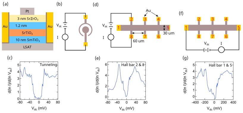
Fig. 1(a) shows a schematic cross-section of the quantum well structure. SrZrO3/SmTiO3/SrTiO3/SmTiO3 films are grown on (La0.3 Sr0.7)(Al0.65Ta0.35)O3 substrates using hybrid MBE, as detailed in Moetakef et al. [27], Zhang et al. [28]. SrZrO3 is deposited between the top SmTiO3 layer and Pt top-gate electrodes as a tunneling barrier for top-gated tunneling devices. Electrical contact to the SrTiO3 is achieved by Ar-ion etching (60 nm) followed by Ti/Au deposition (nm/nm). Both SrTiO3/SmTiO3 interfaces contribute 3.410 electrons to the quantum well, leading to an expected total doping density of [27, 29].
In order to probe transport properties, the quantum well heterostructure is patterned into vertical and lateral transport structures (Figs. 1(b,d)). Current-voltage (I-V) measurements are performed between several pairs of contacts in channels in a dilution refrigerator capable of measuring electrical properties at temperatures ranging from 50 mK to 300 K. Differential conductance spectra d/d vs and normalized conductance [35] are obtained via numerical differentiation.
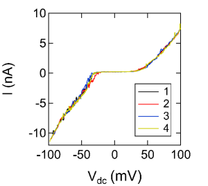
In both vertical and horizontal geometries, the normalized conductance at = 50 mK (Fig. 1(c,e,g)) shows a suppression around zero bias, consistent with previous reports of pseudogap behavior [32]. Here we use the local maxima of the coherence peaks in the vertical geometry to estimate a pseudogap energy meV, based on Fig. 1(c). In both vertical and lateral geometries, there are portions of the circuit in which carriers move in the plane, which complicates the analysis. Generally, the measured pseudogap is expected to over-estimate the intrinsic gap due to voltage drops in the plane. Other reported signatures, e.g., current fluctuations near the threshold for conduction (Fig. 2), are also observed. Similar potential fluctuations were reported by Hardy et al. [36].
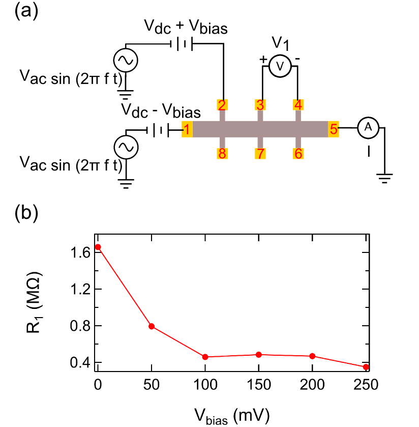
Non-local non-equilibrium four-terminal conductance measurements are conducted using the setup shown in Fig. 3(a). At one of the channel, a combination of differentially applied dc voltage and common-mode dc+ac voltage sin(2 is applied, while the resulting ac voltage and current . The resistance (Fig. 3(b)) for = 20 mV, frequency = 13 Hz, and = -40 mV. decreases by a factor of four as is increased from 0 mV to 100 mV, and is relative stable for 100 mV . This characteristic voltage is comparable to the characteristic pseudogap voltage measured in Fig. 1(f,g). The quantum well system is driven out of equilibrium by a differentially applied voltage , which induces a current between the two electrodes, while the resulting change in resistance along the main channel is measured “downstream“ by driving with the combination of a sinosoidal voltage source and a low dc bias and monitoring the resulting current at electrode 5 and the voltage drop between electrodes 3 and 4. The measurements are non-local because changes in four-terminal conductance are influenced by an excitation in a region outside of where is measured.
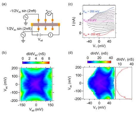
We expand our transport measurements in the channel structure using an experimental setup illustrated in Fig. 4(a). The left side of the channel (electrodes 2 and 8) is driven driven differentially with amplitude and frequency = 1000 Hz, resulting in a net voltage driving across the channel with amplitude . At the same time, a quasi-dc voltage is applied between electrodes 1 and 5, with current measured at electrode 5 and voltage measured between electrodes 3 and 4 (). The two-terminal conductance and four-terminal conductance on the right side of the device are calculated by numerical differentiation as a function of excitation on the left side of the device.
The four-terminal - curves are shown in Fig. 4(b) for various values of . Curves are offset for clarity. A noticeable asymmetry exists in with respect to , in that the magnitude of the current at negative exceeds the value at positive , i.e., . This asymmetry increases as is increased. The two-terminal and four-terminal differential conductances (Fig. 4(c,d)) also show some notable similarities and differences. The parameter range exhibits a low conductance, consistent with the pseudogap behavior shown in Fig. 1(f). The voltage threshold for conductance initially decreases monotonically with , and then begins to increase again. The resulting threshold voltage contour is approximately ellipsoidal with characteristic lobes of decreased conductance when and coincide in magnitude.
The four-terminal conductance (Fig. 4(d)) is decidedly asymmetric, showing a much larger threshold for conduction when 0 than when 0. The asymmetry becomes more pronounced when increases. For example, when =100 mV, the positive threshold for conduction is approximately =50 mV, while the negative threshold is approximately =-20 mV.
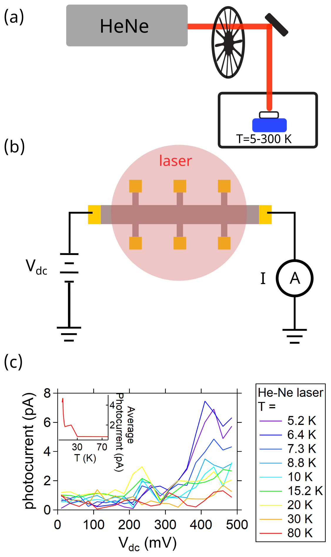
We now examine the effect of optical illumination on transport properties of the SmTiO3/SrTiO3/SmTiO3 channel. Photo-induced current changes in the SmTiO3/SrTiO3/SmTiO3 quantum wells are investigated by illuminating the channel with light from a continuous-wave HeNe laser ( nm, intensity W/m2), modulated at frequency Hz using a mechanical chopper (Fig. 5(a)). Photo-induced current changes are measured versus the dc bias across the channel (Fig. 5(b)). The sample temperature is controlled by an optical cryostat which enables measurements to be conducted between K and K. Non-negligible photocurrent is observed above a voltage threshold of approximately 300 mV, and for temperatures K (Fig. 5(c)).
Discussion.— The non-equilibrium transport measurements probe transport under the presence of various electrical disturbances. The ac voltage driving on the left side of the channel (Fig. 4(a)) produce a non-equilibrium condition that affects transport characteristics on the right side of the channel. The increase in conductance in the region sampled by , brought about by increasing values of , can be interpreted as resulting from quasiparticles excited by that drift into the area between electrodes 3 and 4. Furthermore, the asymmetry of yields insight into the charge of these carriers. For values of exceeding 100 mV, the conductance for sharply exceeds that of its mirror opposite . The implication is that the conductance is larger when negatively charged carriers drift from the left side of the channel to the right side of the channel.
The photocurrent experiments demonstrate the ability of light to produce mobile charge carriers in the pseudogap phase. The optical experiments can be interpreted in a consistent fashion, where the source of the pair breaking arises from light rather than electrical gating. The onset of this photoconductive state coincides in temperature with other transport signatures of the pseudogap phase, and it seems clear that photoexcitation is creating quasiparticles that are immobilized by the pseudogap, and that these carriers live long enough to contribute excess current under suitable voltage bias conditions. The threshold under which photocurrent is observed ( mV) is comparable to the threshold voltage measured in dc transport (Fig. 1(g)), consistent with a scenario that mobile carriers are first photoexcited and subsequently inhibited from recombining by the applied dc bias. The temperature-dependence of the photocurrent provides a signature that the origin of the mobile carriers is linked to the pseudogap phase.
Collectively, the electrical and optical experiments demonstrate that the insulating pseudogap phase is unstable to perturbations that can produce long-lived negatively charged carriers. An obvious interpretation is that these carriers are indeed pre-formed electron pairs, similar to those that have been reported for LaAlO3/SrTiO3 heterostructures and nanostructures [12, 22, 24]. It is therefore plausible that SrTiO3-based quantum well pseudogap behavior arises from electron pairing in the SmTiO3/SrTiO3/SmTiO3 quantum wells. What is unusual is the energy scale, which is at least an order of magnitude larger for the narrow SrTiO3 quantum well.
The experiments described here do not directly point to electron pairing as the origin of the pseudogap phase. They are consistent with this scenario, and suggest follow-up experiments that can more definitively identify the origin of the pseudogap behavior. For example, mesoscopic devices such as single-electron transistors may be able to discern the charge of carriers in the paired and unpaired state. Being able to confirm electron pairing as the origin of the pseudogap in this system would be a remarkable finding, because of the strong connection between quantum confinement and pseudogap energy. Electron pairing at high energies, combined with phase coherence, can potentially lead to the development of engineered structures with unprecedented superconducting transition temperatures.
Acknowledgements.
J.L. acknowledges support from NSF PHY-1913034 and NSF DMR-2225888. S.S. thanks the U.S. Department of Energy for support (Award No. DE-SC0020305).References
- Ding et al. [1996] H. Ding, T. Yokoya, J. C. Campuzano, T. Takahashi, M. Randeria, M. R. Norman, T. Mochiku, K. Kadowaki, and J. Giapintzakis, Nature 382, 51 (1996).
- Loeser et al. [1996] A. G. Loeser, Z. Shen, D. S. Dessau, D. S. Marshall, C. H. Park, P. Fournier, and A. Kapitulnik, Science 273, 325 (1996).
- Timusk and Statt [1999] T. Timusk and B. Statt, Rep. Prog. Phys. 62, 61 (1999).
- Lee et al. [2006] P. A. Lee, N. Nagaosa, and X.-G. Wen, Rev. Mod. Phys. 78, 17 (2006).
- Shimojima et al. [2014] T. Shimojima, T. Sonobe, W. Malaeb, K. Shinada, A. Chainani, S. Shin, T. Yoshida, S. Ideta, A. Fujimori, H. Kumigashira, K. Ono, Y. Nakashima, H. Anzai, M. Arita, A. Ino, H. Namatame, M. Taniguchi, M. Nakajima, S. Uchida, Y. Tomioka, T. Ito, K. Kihou, C. H. Lee, A. Iyo, H. Eisaki, K. Ohgushi, S. Kasahara, T. Terashima, H. Ikeda, T. Shibauchi, Y. Matsuda, and K. Ishizaka, Phys. Rev. B Condens. Matter 89, 045101 (2014).
- Tohyama [2011] T. Tohyama, Jpn. J. Appl. Phys. 51, 010004 (2011).
- Sidorov et al. [2002] V. A. Sidorov, M. Nicklas, P. G. Pagliuso, J. L. Sarrao, Y. Bang, A. V. Balatsky, and J. D. Thompson, Phys. Rev. Lett. 89, 157004 (2002).
- Rossnagel [2011] K. Rossnagel, J. Phys. Condens. Matter 23, 213001 (2011).
- Allen et al. [2015] S. J. Allen, A. J. Hauser, E. Mikheev, J. Y. Zhang, N. E. Moreno, J. Son, D. G. Ouellette, J. Kally, A. Kozhanov, L. Balents, and S. Stemmer, APL Mater. 3, 062503 (2015).
- Stewart et al. [2008] J. T. Stewart, J. P. Gaebler, and D. S. Jin, Nature 454, 744 (2008).
- Jochim et al. [2003] S. Jochim, M. Bartenstein, A. Altmeyer, G. Hendl, S. Riedl, C. Chin, J. Hecker Denschlag, and R. Grimm, Science 302, 2101 (2003).
- Richter et al. [2013] C. Richter, H. Boschker, W. Dietsche, E. Fillis-Tsirakis, R. Jany, F. Loder, L. F. Kourkoutis, D. A. Muller, J. R. Kirtley, C. W. Schneider, and J. Mannhart, Nature 502, 528 (2013).
- Marshall et al. [2015] M. S. J. Marshall, A. E. Becerra-Toledo, L. D. Marks, and M. R. Castell, in Defects at Oxide Surfaces, edited by J. Jupille and G. Thornton (Springer International Publishing, Cham, 2015) pp. 327–349.
- Božović and Levy [2020] I. Božović and J. Levy, Nat. Phys. 16, 712 (2020).
- Randeria and Taylor [2014] M. Randeria and E. Taylor, Annual Review of Condensed Matter Physics 5, 209 (2014).
- He et al. [2011] R.-H. He, M. Hashimoto, H. Karapetyan, J. D. Koralek, J. P. Hinton, J. P. Testaud, V. Nathan, Y. Yoshida, H. Yao, K. Tanaka, W. Meevasana, R. G. Moore, D. H. Lu, S.-K. Mo, M. Ishikado, H. Eisaki, Z. Hussain, T. P. Devereaux, S. A. Kivelson, J. Orenstein, A. Kapitulnik, and Z.-X. Shen, Science 331, 1579 (2011).
- Schooley et al. [1964] J. F. Schooley, W. R. Hosler, and M. L. Cohen, Phys. Rev. Lett. 12, 474 (1964).
- Koonce et al. [1967] C. S. Koonce, M. L. Cohen, J. F. Schooley, W. R. Hosler, and E. R. Pfeiffer, Physical Review 163, 380 (1967).
- Pai et al. [2018] Y.-Y. Pai, A. Tylan-Tyler, P. Irvin, and J. Levy, Rep. Prog. Phys. 81, 036503 (2018).
- Reyren et al. [2007] N. Reyren, S. Thiel, A. D. Caviglia, L. F. Kourkoutis, G. Hammerl, C. Richter, C. W. Schneider, T. Kopp, A. S. Ruetschi, D. Jaccard, M. Gabay, D. A. Muller, J. M. Triscone, and J. Mannhart, Science 317, 1196 (2007).
- Caviglia et al. [2008] A. D. Caviglia, S. Gariglio, N. Reyren, D. Jaccard, T. Schneider, M. Gabay, S. Thiel, G. Hammerl, J. Mannhart, and J. M. Triscone, Nature 456, 624 (2008).
- Cheng et al. [2015] G. Cheng, M. Tomczyk, S. Lu, J. P. Veazey, M. Huang, P. Irvin, S. Ryu, H. Lee, C. B. Eom, C. S. Hellberg, and J. Levy, Nature 521, 196 (2015).
- Prawiroatmodjo et al. [2017] G. E. D. K. Prawiroatmodjo, M. Leijnse, F. Trier, Y. Chen, D. V. Christensen, M. von Soosten, N. Pryds, and T. S. Jespersen, Nat. Commun. 8, 395 (2017).
- Annadi et al. [2018] A. Annadi, G. Cheng, H. Lee, J.-W. Lee, S. Lu, A. Tylan-Tyler, M. Briggeman, M. Tomczyk, M. Huang, D. Pekker, C.-B. Eom, P. Irvin, and J. Levy, Nano Lett. 18, 4473 (2018).
- Briggeman et al. [2020] M. Briggeman, M. Tomczyk, B. Tian, H. Lee, J.-W. Lee, Y. He, A. Tylan-Tyler, M. Huang, C.-B. Eom, D. Pekker, R. S. K. Mong, P. Irvin, and J. Levy, Science 367, 769 (2020).
- Jackson and Stemmer [2013] C. A. Jackson and S. Stemmer, Phys. Rev. B Condens. Matter 88, 180403 (2013).
- Moetakef et al. [2012] P. Moetakef, C. A. Jackson, J. Hwang, L. Balents, S. J. Allen, and S. Stemmer, Phys. Rev. B Condens. Matter 86, 201102(R) (2012).
- Zhang et al. [2014] J. Y. Zhang, C. A. Jackson, R. Chen, S. Raghavan, P. Moetakef, L. Balents, and S. Stemmer, Phys. Rev. B Condens. Matter 89, 075140 (2014).
- Mikheev et al. [2015] E. Mikheev, B. Himmetoglu, A. P. Kajdos, P. Moetakef, T. A. Cain, C. G. Van de Walle, and S. Stemmer, Appl. Phys. Lett. 106, 062102 (2015).
- Jackson et al. [2014] C. A. Jackson, J. Y. Zhang, C. R. Freeze, and S. Stemmer, Nat. Commun. 5, 4258 (2014).
- Stemmer and Allen [2018] S. Stemmer and S. J. Allen, Rep. Prog. Phys. 81, 062502 (2018).
- Marshall et al. [2016] P. B. Marshall, E. Mikheev, S. Raghavan, and S. Stemmer, Phys. Rev. Lett. 117, 046402 (2016).
- Ahadi and Stemmer [2017] K. Ahadi and S. Stemmer, Phys. Rev. Lett. 118, 236803 (2017).
- Joshua et al. [2012] A. Joshua, S. Pecker, J. Ruhman, E. Altman, and S. Ilani, Nat. Commun. 3, 1129 (2012).
- Lang [1986] N. D. Lang, Phys. Rev. B Condens. Matter 34, 5947 (1986).
- Hardy et al. [2017] W. J. Hardy, B. Isaac, P. Marshall, E. Mikheev, P. Zhou, S. Stemmer, and D. Natelson, ACS Nano 11, 3760 (2017).