Monolayer WS2 electro- and photo-luminescence enhancement by TFSI treatment
Abstract
Layered material heterostructures (LMHs) can be used to fabricate electroluminescent devices operating in the visible spectral region. A major advantage of LMH-light emitting diodes (LEDs) is that electroluminescence (EL) emission can be tuned across that of different exciton complexes (e.g. biexcitons, trions, quintons) by controlling the charge density. However, these devices have an EL quantum efficiency as low as10-4%. Here, we show that the superacid bis-(triuoromethane)sulfonimide (TFSI) treatment of monolayer WS2-LEDs boosts EL quantum efficiency by over one order of magnitude at room temperature. Non-treated devices emit light mainly from negatively charged excitons, while the emission in treated ones predominantly involves radiative recombination of neutral excitons. This paves the way to tunable and efficient LMH-LEDs.
Transition metal dichalcogenide monolayers (1L-TMDs) are ideal to study light-matter interactions and many-body effects at the atomic scale[1, 2, 3]. Compared to bulk semiconductors[2], the reduced dielectric screening combined with the spatial confinement of charge carriers[1] favours the formation of various excitonic complexes which can be controlled by modulation of the carrier density[1, 2, 3, 4, 5, 6, 7, 8]. Thus, 1L-TMDs photoluminescence (PL) spectra host features arising from formation of charged[4, 5, 6, 7, 8] and neutral[9, 10, 11, 12] exciton complexes.
Layered material heterostructures (LMHs) combining single layer graphene (SLG), 1L-TMDs, and hexagonal boron nitride (hBN), from 1L-hBN to hundreds of layers, are promising for electronics[13, 14], photonics[15], and optoelectronics[16, 17]. Direct bandgap 1L-TMDs and LMHs can be used to make light-emitting diodes (LEDs)[18, 19, 20, 21, 22, 23, 24, 25, 26, 27], with fast modulation speed (up to GHz)[7, 25, 28], and emission wavelength tunability[7, 25, 6] besides multi-spectral (visible618nm[22, 21, 23] to near-infrared1160nm[29, 30]) emission.
In 1L-TMD-based LEDs, the electroluminescence (EL) efficiency (), i.e. ratio between emitted photons and injected electrons (e)[19, 20], depends on the optical emission of the material[31, 32, 33, 34, 35, 30, 36, 37], as well as on its doping level[38, 6, 39, 40, 41]. In doped 1L-TMDs, the PL and EL emission originates from either negative (X-)[28, 38, 33, 34] or positive (X+)[6, 19, 20] trions, depending on the type of doping. However, 1L-TMD-LEDs based on trionic emission show low (typically0.05%[19, 20]) with respect to neutral exciton (X0) emission (typically 1%[31, 32, 7, 38, 6, 39]). This difference in occurs due the small (30meV) binding energy of trions[42]. Since the X- binding energy is close to the lattice thermal energy at room-temperature (RT=300K,25.2meV), trions dissociate[2]. An excess of free-carriers decreases the available phase-space filling for exciton complexes, due to Pauli blocking, with a reduction of trion and exciton binding energies[43] and oscillator strengths[44] (i.e. the probability of absorption/emission of electromagnetic radiation[45]).
In 1L-TMDs, low light-emission efficiency is observed in both EL (10-4[33, 34] to1%[31, 32, 7, 38, 6, 39]) and PL ( 10-3[36, 40] to5%[1, 2, 3]). is defined as the ratio between emitted and absorbed photons[19, 20]. Thus, several chemical approaches were suggested to enhance , such as treatment with 2,3,5,6-tetrafluoro 7,7,8,8-tetracyanoquinodimethane[46], hydrogen peroxide[47], titanyl phthalocyanine[48], sulfuric acid[49], oleic acid[52, 50, 51], and the superacid (i.e. with acidity greater than that of 100% pure sulfuric acid[53]) bis-(trifluoromethane)sulfonimide (TFSI)[54, 55, 56, 57, 58, 59, 60, 61, 62, 63, 64, 65, 66]. TFSI treatment increased the PL intensity of 1L-WS2 up to10-times[54, 56, 55, 52] due to depletion of excess e, promoting X0 recombination.
The effect of chemical passivation of 1L-TMDs on combined with gated-PL emission in 1L-TMD-based LEDs was not reported to date, to the best of our knowledge. Refs.[54, 55, 56, 57, 58, 59, 60, 61] reported PL measurements on 1L-TMDs and focused on non-gated samples, thus limiting the modulation of charge density in 1L-TMDs. Ref.[8] performed gated-PL measurements in 1L-WS2, finding that both TFSI treatment and electrical gating increase by a factor of up to10 (at1019cm-2s-1 photocarrier generation rate), because both processes reduce the n-type behaviour of 1L-WS2 and suppress X- formation, thus enhancing X0 radiative recombination. However, gated-PL measurements after TFSI passivation were not provided. The activation of trapping states on TFSI-treated 1L-TMDs was not discussed. Ref.[67] carried out EL experiments with TFSI passivation for high-speed (MHz) modulation, but did not report PL nor EL emission tunability. Therefore, an investigation on how TFSI affects EL emission and modifies gated-PL of 1L-TMD-based devices is required.
Here, we fabricate LEDs with 1L-WS2 as active material on a metal-insulator-semiconductor (MIS) structure. We measure EL and gated-PL before and after TFSI treatment. We find that TFSI increases by over one order of magnitude at RT, and PL intensity by a factor5. We find that X- and X0 are present in both EL and PL before TFSI treatment, whereas X0 dominates after. We attribute this to depletion of excess e and changes in the relaxation pathway, induced by the treatment. This paves the way to more efficient 1L-TMDs-based LEDs and excitonic devices.
I Results and Discussion
We use 1L-WS2 as the active light-emitting layer since it has a direct bandgap[68, 69, 70, 71], its PL emission is60 times stronger than 1L-MoS2[69, 39] at RT, can be up to50 times larger than 1L-MoS2[19, 20] at RT, while Refs.[52, 54, 55, 56, 57, 58, 59, 60, 61, 62, 63, 64, 65] demonstrated that TFSI treatment increases up to10-times its PL intensity.
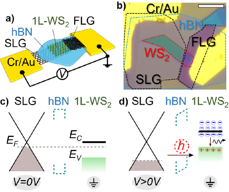
Fig.1a shows the 1L-WS2/hBN/SLG tunnel junction configuration used here, where the metallic electrodes provide contacts to apply a voltage (V) between SLG and 1L-WS2. This is prepared as follows.
WS2 crystals are synthesized using a two-step self-flux technique[72] using 99.9999% purity W and S powders without any transporting agents. Commercial (Alfa Aesar) sources of powders contain a number of defects and impurities (Li, O, Na, and other metals as determined by secondary ion mass spectroscopy). Before growth, W and S powders are thus purified using electrolytic[73] and H2[73] based techniques to reach 99.995% purity. WS2 polycrystalline powders are created by annealing a stoichiometric ratio of powders at 900∘C for 3 weeks in a quartz ampoule sealed at 10-7 Torr. The resulting powders are re-sealed in a different quartz ampoule under similar pressures and further annealed at 870-910∘C with thermodynamic temperature differential (hot to cold zone difference)40∘C. The growth process takes 5 weeks. At the end of the growth, ampoules are cooled to RT slowly (40∘C/hour)[74]. We use this material as bulk source because our previous work[74] demonstrated that this has a point defect density109-1010 cm-2, on par or better than previous reports[75].
Bulk WS2, hBN (grown by the temperature-gradient method[76]), and graphite (sourced from HQ Graphene) crystals are then exfoliated by micromechanical cleavage using Nitto-tape[77] on 285nm SiO2/Si. Optical contrast[78] is first used to identify 1L-WS2, SLG, FLG (3-10nm), and hBN(5nm). The LMs are then characterized by Raman spectroscopy as discussed in Methods. After Raman characterization of all individual LMs on SiO2/Si, the FLG/1L-WS2/hBN/SLG LMH is assembled using dry-transfer as for Refs.[79, 80]. FLG is picked-up from SiO2/Si using a polycarbonate (PC) membrane on a polydimethylsiloxane (PDMS) stamp (as mechanical support) at 40∘C. We use 40∘C because this is sufficient to increase the adhesion of the PC film[81], to pick all LMs from SiO2/Si. Then, FLG is aligned to one edge of 1L-WS2 on SiO2/Si and brought into contact using xyz micromanipulators at 40∘C, leaving the majority of 1L-WS2 without FLG cover to be used as active area (AA). AA is the region from where light emission is expected, and it is the overlap area between 1L-WS2 and SLG (green-shaded part in Fig.1b). Next, FLG/1L-WS2 is aligned to a hBN flake deposited onto SiO2/Si and brought into contact using xyz micromanipulators at 40∘C. Finally, FLG/1L-WS2/hBN is aligned to a SLG on SiO2/Si and brought into contact using xyz micromanipulators at 180∘C, whereby PC preferentially adheres to SiO2[79], allowing PDMS to be peeled away, leaving PC/FLG/1L-WS2/hBN/SLG on SiO2/Si. PC is then dissolved in chloroform for15mins at RT, leaving the FLG/1L-WS2/hBN/SLG LMH on SiO2/Si[79, 80]. After LMH assembly, Cr/Au electrodes are fabricated by electron beam lithography (EBPG 5200, Raith GMBH), followed by metallization (1:50nm) and lift-off.
The tunnel junction based on a MIS structure consists of a LMH with 1L-WS2 as the light emitter, FL-hBN (typically from 2 to 4nm) acting as tunnel barrier, and a SLG electrode to inject holes (h) into 1L-WS2. We use FL-hBN5nm so that a low (typically5V) driving voltage is sufficient for charge injection to the 1L-WS2[82, 83]. We employ FLG (3-10nm) to contact 1L-WS2, because FLG reduces the contact resistance[84], while Cr/Au electrodes give Ohmic contacts to SLG and FLG[84]. SLG could also be used to contact 1L-WS2, however, as the optical contrast is higher in FLG than SLG[85, 78], using FLG makes it easier to align it to 1L-WS2 during transfer. Since TFSI treatment requires direct exposure of 1L-TMDs[54], we place 1L-WS2 on top of the stack to compare the device performance before and after treatment. We TFSI-treat 4 samples for EL and gated-PL measurements. These are immersed in a TFSI solution (0.2 mg/mL) in a closed vial for 10mins at 100∘C[54, 55, 56], then removed, dried by a N2 gun, and annealed on a hot plate at 100∘C for 5mins[54, 55, 56]. Fig.1b is an image of the 1L-WS2-LEDs. The FLG electrode is placed on the side of the SLG to avoid direct tunneling of carriers from SLG to FLG, hence keeping as AA the LMH region extended over SLG and 1L-WS2, green-shaded in Fig.1b. If there is a FLG/SLG overlap, tunneling through FLG-SLG may be possible, not resulting in e-h recombination into 1L-WS2, hence no EL[25, 38, 6].
Figs.1c,d sketch the band diagram of our LEDs for V=0V and V0V, respectively. For V=0V (at thermodynamic equilibrium as indicated in Fig.1c), the Fermi level, EF, is constant across the junction, and the net current (I) is zero[21, 25, 38, 6, 28]. For V0V (positive potential on SLG), the SLG EF is shifted below the 1L-WS2 valence band energy EV (Fig.1d), and h from SLG tunnel across the hBN barrier into 1L-WS2, promoting EL emission by radiative recombination between the injected excess h and intrinsic e[21, 22, 23, 24, 38, 35, 28]. The EL emission is expected to increase as a function of tunneling current because of the increasing h injected into 1L-WS2 available for e-h recombination.
The LMs are characterized by Raman, PL, EL spectroscopy using a Horiba LabRam HR Evolution. The Raman spectra are collected using a 100x objective with numerical aperture (NA)=0.9, and a 514.5nm laser with a power5W to avoid damage or heating. The voltage bias dependent PL and EL are collected using a long working distance 50x objective (NA=0.45). For the PL spectra, we use a 532nm (2.33eV) laser in order to excite above the X0 emission (2eV)[9, 10]. The power is kept80nW to avoid laser-induced thermal effects[2, 9, 10, 11]. The voltage (V) and current (I) between source (SLG) and drain (1L-WS2) electrodes are set (V) and measured (I) by a Keithley 2400.

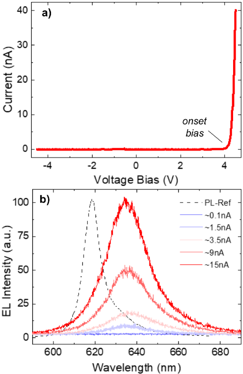
Fig.2 shows the Raman spectrum of 1L-WS2/hBN/SLG on Si/SiO2 after device fabrication and before current-voltage (I-V) measurements. The Raman modes of each LM can be identified. For 1L-WS2, Pos(A) and its full width af half maximum, FWHM(A), change from418.9cm-1; 3.9cm-1, before assembly, to419.8cm-1; 3.4cm-1, after. All the changes in the other modes are close to our spectral resolution and errors, as for Ref.[86]. Pos(A) and FWHM(A) are sensitive to changes in n-doping[87, 88]. The mechanism responsible for this effect is an enhancement of electron-phonon (e-ph) coupling when e populate the valleys at K and Q simultaneously[88]. The energy of the K and Q valleys is modulated by the A ph[88]. Since the K and Q energies are modulated out-of-phase, charge transfer between the two valleys occurs in presence of the A ph[87, 88]. When the K and Q valleys are populated by e, these are transferred back and forward from one valley to the other[88, 89]. This increases the e-ph coupling of out-of-plane modes, such as A[88]. The same process does not occur for p-doping[88]. The reason for this asymmetry between n- and p-doping is due to a much larger energy separation (230meV[88]) between the VB and K valleys than that (100meV[88]) of the CB K and Q valleys. From the changes in Pos(A) and FWHM(A), and by comparison with Ref.[88], we estimate a reduction in n-dopingcm-2.
For hBN in Fig.2, Pos(E2g)1366.4cm-1 and FWHM(E2g)9.2cm-1. Although FWHM(E2g) changes within the error, Pos(E2g) downshifts2.1cm-1 after assembly, suggesting a contribution from strain (see Methods for comparison between FL- and bulk-hBN Raman). Uniaxial strain lifts the degeneracy of the E2g mode and results in the splitting in two subpeaks E and E, with shift rates-8.4 and -25.2cm-1/[90, 91]. For small levels of uniaxial strain (0.5) splitting cannot be observed and the shift rate is-16.8cm[90, 91]. For biaxial strain, splitting does not occur and E2g shifts with rate-39.1cm-1/[90]. Since we do not observe splitting, the E2g shift can be attributed to uniaxial or biaxial tensile strain0.13 or0.06, respectively.
For SLG in Fig.2, no D peak is observed after LMH assembly, indicating negligible defects[92, 94, 93]. In Fig.2 Pos(G)1585.1cm-1, FWHM(G)9.0cm-1, Pos(2D)2692.3cm-1, FWHM(2D)20.9cm-1, I(2D)/I(G)2.4, and A(2D)/A(G)5.6. These indicate that the SLG is p-doped, with E15050meV[95, 94, 93] by taking into account the average dielectric constant (3.85) of the environment (3.8[96] and 3.9[97]). E150meV should correspond to Pos(G)1584.1cm-1 for unstrained SLG[98]. However, Pos(G)1585.1cm-1, which implies a contribution from compressive uniaxial (biaxial) strain0.04 (0.01). The strain level for SLG and hBN are different, most likely due to the fact that the SLG is directly exfoliated onto SiO2/Si, while hBN is picked up and transferred by PDMS stamps, hence, this could induce a larger amount of strain on hBN.
Fig.3a plots the I-V characteristics. For V=0V the current is zero (Fig.1c). When V is applied, an electrical rectification (i.e. diode behavior) with negligible leakage current (I10-11A) for V0 is seen. A tunneling onset, (i.e. exponential increase of I) is seen at VON4.1V, Fig.3a. VON is related to the breakdown electric field (Ebd) across the junction, which depends on the voltage drop on the hBN tunnel barrier and hBN thickness (d) accordingly to Ebd=(Vbd/d)0.7-1V/nm[82, 83], where Vbd is voltage breakdown Vbd=qnd2/(), q is the e charge, n is total charge concentration, =8.85410-12 F/m and 3.9[82, 83], so that VON can vary between different devices. When VVON, h from SLG tunnel across the hBN barrier into 1L-WS2, promoting EL emission by radiative recombination between the injected h and majority e in 1L-WS2 (Fig.1c)[21, 22, 23, 24, 38, 35]. The EL intensity634nm (1.956eV) increases with tunneling current, as in Fig.3b. No light emission is observed in reverse V and small positive (VVON) biases, below the tunneling condition (VON4.1V). A red-shift48meV is observed in EL emission634nm (1.956eV) with respect to the PL X0 emission of the unbiased device (dashed black line, Fig.3b). Fig.3b shows a EL peak position close to X- of unbiased PL (dashed black line, Fig.3b), implying a trionic EL emission, due to excess e in 1L-WS2[38, 28].
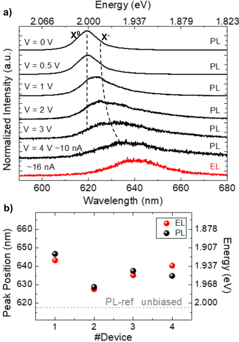
To further understand the EL emission origin, we perform EL and PL spectroscopy at the same V. Fig.4a plots PL spectra at different V. At V=0V, the PL peak is619.2nm (2.002eV), assigned to X0[9, 69]. By increasing V (i.e. increasing e density in 1L-WS2), a second peak appears at longer wavelengths (630nm,1.968eV), due to X-[9, 10, 99, 11]. For V0V, the X0 intensity gradually decreases and nearly vanishes, while X- shifts to longer wavelengths, Fig.4a. This is expected for trionic emission, due to e-doping induced by V[38, 12, 9, 10, 99, 11]. Similar effects were observed in 1L-MoS2/SiO2/Si[101], hBN/1L-WSe2/hBN/SiO2/Si[6], and hBN/1L-WS2/hBN/SiO2/Si[28]. Therefore, for similar tunneling current, EL agrees in energy and shape with the PL emission (see, e.g., the PL and EL spectra at the bottom of Fig.4a). This is confirmed by Fig.4b, where EL and PL peak positions are plotted for 4 devices, showing EL and PL emission at very similar wavelengths. Thus, EL predominantly originates from X-[21, 38, 9, 10, 6]. The variations in X- energy for different LEDs are due to changes in charge carriers density across different samples. E.g., the charge density variation in 1L-WS2 can be due to the number of vacancies in 1L-WS2[41] and external impurities (PC residues and adsorbed water) after LED fabrication, which may vary from sample to sample.
| Peak | Bulk-WS2 Assignment | Bulk-WS2 | 1L-WS2 Assignment | 1L-WS2-SiO2 | 1L-WS2-LMH | TFSI + 1L-WS2-LMH |
|---|---|---|---|---|---|---|
| 1 | LA(M) | 174.5 (11.1) | LA(M) | 175.6 (14.5) | 175.6 (14.6) | 174.9 (14.4) |
| 2 | LA(K) | 194.8 (3.3) | LA(K) | 193.3 (4.5) | 193.8 (3.3) | 193.3 (4.7) |
| 3 | A1g(K)-LA(K) | 213.7 (4.2) | A(K)-LA(K) | 214.5 (5.7) | 214.5 (5.2) | 213.5 (6.0) |
| 4 | A1g(M)-LA(M) | 232.8 (5.7) | A(M)-LA(M) | 231.5 (6.7) | 231.9 (7.1) | 231.4 (5.9) |
| 5 | A1g(M)-ZA(M) | 266.8 (6.9) | A(M)-ZA(M) | 265.3 (6.9) | 265.9 (7.2) | 265.4 (7.0) |
| 6 | E() | 297.6 (4.2) | E() | 297.7 (2.8) | 298.5 (3.1) | 298.7 (2.6) |
| 7 | LA(M)+TA(M) | 311.2(2.4) | LA(M)+TA(M) | 311.2 (2.5) | 311.8 (2.3) | 311.2 (2.4) |
| 8 | E(M) | 324.6 (17.5) | E(M) | 326.7 (25.5) | 325.9 (24.7) | 327.7 (25.7) |
| 2LA(M) | 350.6 (8.3) | 2LA(M) | 352.4 (9.3) | 352.7 (9.2) | 352.7 (8.0) | |
| E() | 356.9 (1.5) | E() | 357.2 (3.3) | 357.4 (3.1) | 357.2 (2.9) | |
| A1g() | 420.8 (2.1) | A() | 418.9 (3.9) | 419.8 (3.4) | 419.9 (3.4) |
We now consider the origin and consequences of excess e in 1L-WS2 for EL emission induced by V. Besides the intrinsic charge carriers in 1L-WS2 (typically n-type due to S vacancies[41]), there is also an electrostatically induced charge in 1L-WS2 when V0V. A SLG/hBN/1L-WS2 tunneling junction acts as a MIS capacitor[38, 6, 28]. When V0 is applied to SLG, inducing positive charges in SLG, there is an opposite (negative) charge induced in 1L-WS2[38, 6, 28], thus making the charge density on 1L-WS2 larger than for V0. When VVON, h will be injected by tunneling into 1L-WS2 (Fig.1d), hence, h will recombine with e. Consequently, the EL emission originates from X- states. However, the radiative recombination efficiency (defined as the number of e-h pairs that recombine by emission of a photon divided by total number of e-h pairs) of X- is lower than X0 because of the small (30meV) binding energy of trions[42]. Thus, to gain higher one should favor X0 EL emission by lowering the unbalanced free-carriers concentration in 1L-TMDs by either gate modulation[38, 6, 28, 12, 31, 36], physical[102, 103], or chemical doping[25, 11].
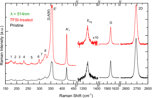
We thus treat 1L-WS2 using TFSI to reduce doping and favor X0 emission under bias and investigate the effects on EL emission and gated-PL. Fig.5 plots representative Raman spectra before (black) and after (red) TFSI treatment. By comparing the spectra before and after TFSI treatment, and the fits for the 1L-WS2 in Table 1, we do not observe significant changes in peak position and FHWM. However, there is an overall intensity increase of the Raman modes of50, compared to the Si peak. This indicates a reduction of n-doping induced by TFSI treatment, because S vacancies in 1L-TMDs are commonly associated to n-type behaviour and the reduction of these defects will reflect in p-type doping fingerprint[54, 55, 56, 66]. Pos(A) is unaffected by TFSI treatment, which suggests that the reduction in the intrinsic 1L-WS2 n-doping induced by TFSI is1012cm-2[88]. Although TFSI is able to p-dope SLG when it is in contact with the TFSI solution[104], Fig.5 shows negligible (within the errors[86]) changes in the SLG (e.g. before (after): Pos(G)1585.1 (1585.0)cm-1, FWHM(G)9.0 (9.1)cm-1, Pos(2D)2692.3 (2692.2)cm-1, FWHM(2D)20.9 (20.8)cm-1, I(2D)/I(G)2.4 (2.4), and A(2D)/A(G)5.6 (5.6)) and hBN (e.g. before (after): Pos(E2g)1366.4 (1366.5)cm-1 and FWHM(E2g)9.2 (9.1)cm-1) Raman spectra after treatment, as both are protected by the top 1L-W2.
Fig.6a plots a representative PL spectrum of 1L-WS2 embedded in the LMH before TFSI treatment, and Fig.6b after treatment. For the pristine case, there are two components, fitted by two Lorentzians618.7nm (2.004eV) and629.1nm (1.971eV) corresponding to X0[71, 69] and X- emission[99, 100]. For non-biased devices, the spectral weight (defined as the area of each peak) of the PL emission indicates a majority emission due to X0. After treatment, the PL emission evolves to a main single peak618.1nm (2.006eV), accompanied by a4-fold increase in PL intensity. The changes in spectral weight of X0 and X- emission after treatment can be assigned to a reduction in the e-density in 1L-WS2[54, 55, 56], in agreement with our Raman analysis. Refs.[52, 50, 51, 54, 55, 56, 57, 58, 59, 60, 61, 62, 63, 64, 65] reported that PL enhancement depends on sample quality (defects) and may vary 1 to 10 times. In our samples we observe a PL increase51-times, consistent with Refs.[52, 50, 51, 54, 55, 56, 57, 58, 59, 60, 61, 62, 63, 64, 65].
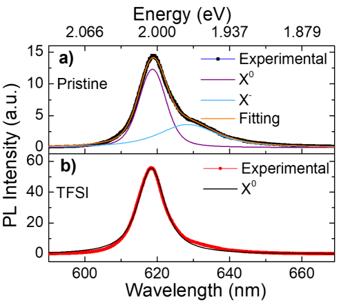
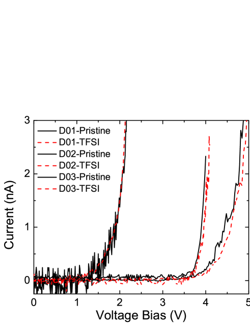
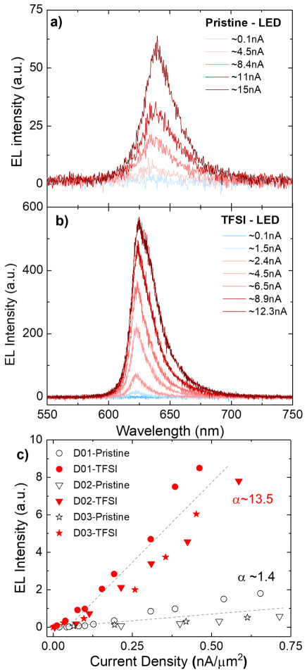
Fig.7a plots typical I-V characteristics of 3 devices before (solid black lines) and after (dashed red lines) TFSI treatment. I is not affected by the treatment. VON is mostly influenced by the hBN thickness[82, 83]. Figs.8a,b show EL collected before and after TFSI, respectively, for different I. In both cases, EL is triggered for similar current levels (I5nA), and the intensity increases linearly with I, Fig.8c. The EL intensity slope as a function of current density (I divided by AA) is affected by TFSI. For pristine-LEDs we get an average slope 1.40.3, while after TFSI 13.51.1, with 1 order of magnitude increase, Fig.8c. The red-shifts in the EL emission with I increase in pristine (6nm) and TFSI treated LEDs (5nm), Figs.8a,b, can be assigned to EF shift induced by the MIS structure[31, 6, 33].
Next, we estimate the external quantum efficiency (EQE) of our LEDs. This is defined as the ratio between the number of emitted photons (Nph) and that of injected h per second (Nh)[105]:
| (1) |
where is the sum of the total photons collected by the spectrometer over the measured spectral range, Aeff=AA/Aspot, where Aspot is the microscope objective spot size (Aspot=/2NA]2 2.2m2, with =618nm and NA=0.45), and =It/q, where t is the acquisition time, and q the e charge. The efficiency factor (defined as the ratio between the photons collected by the detector and the emitted photons by EL at the sample position) of our setup, including all optical components and spectrometer, is 0.0051, see Methods.
From Eq.1 we get EQE0.025%0.021% and0.195%0.324% for pristine- and TFSI treated-LEDs, respectively, corresponding to a8.71.5-fold increase, thus demonstrating that TFSI can boost EQE by almost one order of magnitude. It was reported that, using pulsed (AC) bias, EL emission can be enhanced a factor4[33] and up to100 in a double optical cavity (distributed Bragg reflector (DBR) with an optical mirror)[106]. Therefore, AC bias and photonic cavities could be combined with TFSI treatment to achieve EQE10 in 1L-TMDs.
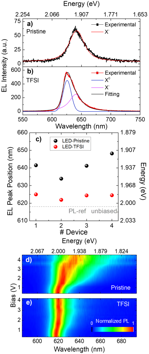
We now consider the EL emission features induced by TFSI treatment. By comparing EL before and after TFSI (Figs.8a,b), a blue-shift in EL is observed. In pristine-LEDs, the EL emission is641.8nm (1.931eV), Fig.9a, whereas after treatment it is625.6nm (1.982eV), Fig.9b. Fig.9c plots the EL peak position before and after treatment in 4 devices. After treatment, the EL emission shifts to shorter wavelengths, where X0 is expected[68, 69] (dashed line in Fig.9c). In non-biased S-based TMDs devices, this shift could be due to the depletion of excess e in n-doped 1L-WS2 due to TFSI[54, 55, 56, 57, 58, 59, 62, 63, 64]. Nevertheless, we cannot neglect the additional charge density induced by V on the MIS capacitor. E.g. the I-V characteristics in Fig.7 show that I and VON do not change before and after TFSI, suggesting the same tunneling condition is maintained across the 1L-WS2/hBN/SLG junction. In both cases a comparable electric field (and electric charge) is developed across the junction for a given V. Fig.7 implies that, independent of TFSI treatment, the same amount of negative charge is electrostatically induced in 1L-WS2 at V0. However, taking into account the EL spectral shift towards X0 emission upon bias, the expected depletion of excess e in 1L-WS2 cannot explain the electrical behaviour of Figs.9b,c. Consequently, the emission profile is not compatible with the I-V curves before and after TFSI in Fig.7, given that the electric field across the junction should be modified by the e density change in 1L-WS2.
To get a better insight on the effects of TFSI on 1L-WS2 based LEDs, Figs.9d,e plot normalized PL spectra as a function of V before and after TFSI. In the pristine case (Fig.9d), the PL map shows an evolution in emission spectra from620nm (2.000eV) to638nm (1.943eV), corresponding to a spectral shift from X0 to X- due to excess e in 1L-WS2 induced by V. After TFSI treatment (Fig.9e), the PL exhibits only a minor shift from618nm (2.006eV) to622nm (1.993eV), implying that the induced e-charge in 1L-WS2 does not contribute to the X- emission pathway. Therefore, similar to Figs.9a,b, PL also indicates that the emission after TFSI treatment predominantly originates from radiative recombination of X0, independent of V. Refs.[54, 56, 58, 59, 60, 61] claimed that TFSI treatment reduces the extent of n-type behavior in S-based 1L-TMDs due to S vacancies passivation, consistent with the suppression of X- formation in Refs.[57, 62, 63, 64, 65]. Ref.[8] reported that TFSI acts as a Lewis acid, i.e. it can accept an e pair from a donor[53], suppressing X- formation. Whereas Refs.[52, 50, 51] claimed that TFSI may activate sub-gap states and reduce the n-type behavior in S-based TMDs, as well as reducing X- formation. Our I-V, EL and gated-PL results suggest that TFSI treatment i) depletes the excess e in 1L-WS2, acting as a Lewis acid[8] and ii) favours the radiative recombination of X0 independent of bias, due to the activation of trapping states[50, 52] in 1L-WS2 caused by the treatment. One would expect changes in the excitonic emission at such trapping states at RT, where the thermal energy can assist carrier de-trapping, and radiative recombination from excitons[64]. Therefore, the modification from non-radiative to radiative recombination by activation of trapping states could be further engineered to achieve more efficient optoelectronic devices.
II Conclusions
We demonstrated a one order of magnitude enhancement in EL emission of 1L-WS2-LEDs by performing TFSI treatment. EL predominantly originates from trions in pristine devices, while neutral excitons dominate in treated ones. The neutral excitonic emission is also restored in 1L-WS2 gated-PL measurements. We attribute these changes to a reduction of n-doping of 1L-WS2, as well as changes in the relaxation and recombination pathways within 1L-WS2. This paves the way to more efficient 1L-TMDs-based LEDs, and shed light into tunability of the excitonic emission of these devices.
III Methods
III.1 Raman characterization of LMH individual constituents
Raman spectroscopy allows us to monitor LMs at every step of device fabrication. This should always be performed on individual LMs before and after assembly in LMHs and devices. This is an essential step to ensure reproducibility of the results, but, unfortunately, this is often neglected in literature.
Ultralow-frequency (ULF) Raman spectra in the range10-50cm-1 probe shear (C), corresponding to layer motion parallel to the planes, and layer breathing modes (LBM), corresponding to the motion perpendicular to them[107, 108, 109, 93]. Pos(C)N can be used to determine the number of layers[107, 108, 109] as N=, with Pos(C)∞ the bulk Pos(C).
Fig.10 plots the Raman spectra of non-treated 1L-WS2 and bulk-WS2. In Fig.10a, the C mode and LBM are not observed for 1L-WS2, as expected[107, 108, 109]. In bulk-WS2, Pos(C)cm-1. The spectral resolutioncm-1 for the ULF region is obtained as for Ref.[86]. We observe two additional peaks28.7cm-1 and 46.4cm-1, respectively, in agreement with Refs.[110, 111, 112]. These do not depend on N[110, 111] and are seen because 514.5nm (2.41eV) is nearly resonant with the B exciton (2.4eV) of 1L-WS2[113, 114, 115, 116, 117], and20meV above the bulk-WS2 B exciton (2.38eV)[114, 115]. This gives rise to a resonant process[113, 114, 115, 116, 117], which occurs because the laser energy matches the electronic transition of the B exciton, revealing features associated with intervalley scattering mediated by acoustic ph[118, 119, 120]. A similar process also happens in 1L-MoS2[110, 111] and other 1L-TMDs[118, 119, 120]. Although our ULF filters cut5cm-1, the LBM is not detected in bulk-WS2, as its frequency is expected to be10cm-1[109], because this resonant process with a 514.5nm laser reduces the signal to noise ratio in this spectral region[110].
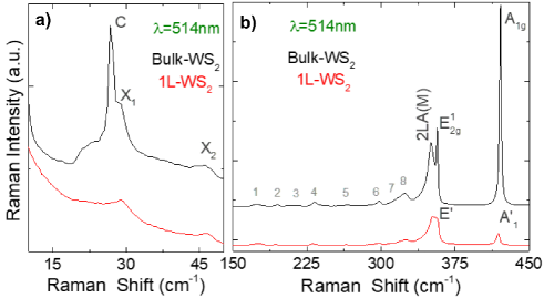
The high-frequency (HF) Raman spectra of non-treated 1L-WS2 and bulk-WS2 (Fig.10b) show various peaks, Table 1. The first order Raman modes, i.e. E, A in 1L-WS2[68, 69, 70, 71] and E, A1g in bulk-WS2[68, 69, 70, 71]. E (E) and A (A1g) correspond to in-plane and out-of-plane optical ph for 1L(bulk)-WS2. Their nomenclature for 1L and bulk differs due to the different crystal symmetry[68, 69, 70, 71]. In 1L-WS2 we get Pos(E)356.8cm-1, FWHM(E3.2cm-1, Pos(A)418.5cm-1, FWHM(A)4.3cm-1. In bulk-WS2 we have Pos(E)356.8cm-1, FWHM(E)1.5cm-1, Pos(A)420.8cm-1, FWHM(A)2.1cm-1. In 1L-WS2 the difference in peaks’ position [Pos(E)-Pos(A)] is61.7cm-1 while this is64.0cm-1 in bulk-WS2, further corroborating the identification of 1L[68]. In the HF spectra of 1L- and bulk-WS2 we also observe the 2LA(M) mode, involving two longitudinal acoustic (LA) ph close to the M point[68, 69, 70]. For 1L-WS2 Pos(2LA(M))351.9cm-1 and FWHM(2LA(M))9.2cm-1, whereas for bulk-WS2 Pos(2LA(M))350.6cm-1 and FWHM(2LA(M))8.3cm-1. The 2LA(M) mode originates from a second-order double resonant process[118, 119, 120], where momentum conservation is satisfied by two LA ph with opposite momenta around K- and M-points[119], therefore sensitive to differences in band structure between bulk and 1L-WS2[68, 121].
I(A1g)/I(E1g)3.2 in bulk-WS2, where I is the peak height, is higher than I(A)/I(E)0.8 in 1L-WS2. I(2LA)/I(E1g)1 in bulk-WS2 is lower than I(2LA(M))/I(E)1.7 in 1L-WS2. This can be explained considering that the main first-order (E, A) and second-order (2LA(M)) Raman modes are enhanced for 2.41eV excitation, due to exciton-ph coupling effects involving B exciton transitions[116, 122]. These depend on mode symmetry (i.e. differ between out-of-plane and in-plane modes) as well as N[118]. In bulk-WS2, the out-of-plane A1g is resonant with the B exciton, unlike E[118]. The enhancement of A1g decreases with decreasing N due to the dependence of the lifetime of the intermediate excitonic states on N[118]. The difference between I(2LA)/I(E) in 1L-WS2 and I(2LA)/I(E) in bulk-WS2 is due to a change in band structure from direct bandgap in 1L to indirect in bulk-WS2[68, 69, 70, 71], which changes the double resonance conditions[118, 119, 120].
The Raman spectrum of 1L-WS2 also shows 8 peaks in the range 170-350cm-1 (Fig.10b and Table 1). LA(M) and LA(K) correspond to one-ph processes originating from the LA branch at the M- and the K-points, respectively[68, 69, 70, 71]. Since LA(M) and LA(K) and E(M) are one-ph processes from the edge of the BZ (q0)[68, 69, 70, 71], they should not be seen in the Raman spectra since, due to the Raman fundamental selection rule[123], one-ph processes are Raman active only for ph with q0, whereas for multi-ph scattering the sum of ph momenta needs to be0[118, 119, 120, 121]. However these modes can be activated in presence of defects, as these can exchange momentum with ph, such that the sum of the momenta in the process is0[68, 69, 70, 71]. A1g(K)-LA(K), A1g(M)-LA(M), A1g(M)-ZA(M), LA(M)+TA(M) in bulk-WS2 and A(K)-LA(K), A(M)-LA(M), A(M)-ZA(M), LA(M)+TA(M) in 1L-WS2 are combinational modes, and Raman allowed[68, 69, 70, 71]. E(M) correspond to a one-ph process originating from the transverse optical (TO) branch at the M-point[68, 69, 70, 71]. E() is a degenerate mode originating from the LO and TO branches at [68, 69, 70, 71].
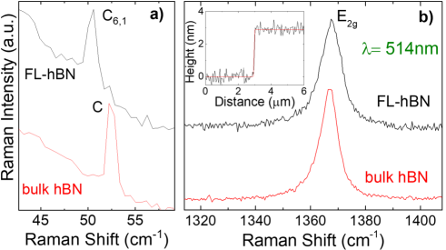
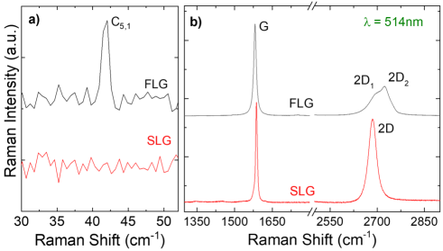
Fig.11 plots the Raman spectra of a3nm hBN flake (black curves) and bulk-hBN (red curves). The latter has 2 Raman-active modes[124, 125], C and E2g. In Fig.11a Pos(C)∞=52.30.14cm-1 with FWHM0.7cm-1 for bulk-hBN and Pos(C)N=50.40.14cm-1 FWHM0.8cm-1 for the hBN flake. In bulk-hBN Pos(C)∞= =52.3cm-1, with =6.91027kg the mass of one layer per unit area, c the speed of light in cm s-1, and the spring constant associated to the coupling between the adjacent layers[86, 109]. From this, we get Nm-3. From N=, we get N=61 for the 3nm thick flake (measured with a Dimension Icon Bruker AFM in tapping mode) as shown in the inset of Fig.11b). In Fig.11b Pos(E2g)1368.5cm-1 and FWHM(E2g)9.1cm-1 for FL-hBN, and Pos(E2g)1367cm-1 with FWHM(E2g)7.6cm-1 for bulk-hBN. The peak broadening1.5cm-1 in FL-hBN can be attributed to strain variations within the laser spot, as thinner flakes conform more closely to the roughness of the underlying SiO2[86]. This is consistent with the fact that thicker hBN have lower root mean square (RMS) roughness[86, 79, 126, 83], e.g. 300nm SiO2 has RMS roughness1nm[83], 2-8nm hBN has RMS roughness0.2-0.6nm[86], while10nm hBN thick presents RMS roughness0.1nm[79, 83].
The red curves in Figs.12a,b are the Raman spectra of SLG on SiO2/Si before LMH assembly. Pos(G)=1586.9cm-1 with FWHM(G)=7.7cm-1, Pos(2D)=0.2cm-1 with FWHM(2D)29.3cm-1, I(2D)/I(G)0.85, A(2D)/A(G)3.3. These indicate a p-doping[95, 94, 93] with E50meV. No D peak is observed, thus negligible defects[92, 94, 93]. Pos(G) and Pos(2D) are affected by the presence strain[94, 93]. Biaxial strain can be differentiated from uniaxial from the absence of G-peak splitting with increasing [127, 128], however at low (0.5%) the splitting cannot be resolved[127, 128]. Thus, the presence (or coexistence) of biaxial strain cannot be ruled out. For uniaxial(biaxial) strain, Pos(G) shifts by Pos(G)/ 23(60)cm-1/%[127, 128]. Pos(G) also depends on doping[98, 95]. E50meV should correspond to Pos(G)1584.3cm-1 for unstrained SLG[98]. However, in our experiment Pos(G)1586.9cm-1, which implies a contribution from compressive uniaxial (biaxial) strain0.1% (0.04%). The black curves in Figs.12a,b show the Raman spectrum of the FLG electrode on SiO2/Si. Pos(G)0.2cm-1 with FWHM12cm-1, Pos(2D1)0.2cm-1 with FWHM48cm-1, and Pos(2D2)0.2cm-1 with FWHM33cm-1. Pos(C)41.4cm-1, corresponding to N=5.
III.2 Spectrometer efficiency
The of our spectrometer is derived as follows. We use a 50x objective (NA=0.45). Hence, the solid angle is =(1-cos)2, where =arcsin(NA/n), and n is the refractive index. Assuming n=1 we get =0.672. Thus, M50x-eff=/(4)100%5.4%. In our Horiba system, the optical path from M50x to CCD includes 7 Mirrors (M83%), a slit (S90%), a grating (G60%) and a CCD detector (CCD85%). Therefore, the calculated overall collection+Horiba efficiency is: M(Meff)SGCCD0.0067. To experimentally validate the calculation, we use a 0.5pW laser at 632.8nm and measure the counts at the CCD detector Ncounts=149748. The photon energy at 632.8nm is Eph=(1.24/0.638)1.6e-19=3.13e-19J. The laser power is Popt=0.5e-12 J/s. As a result, if the system efficiency is 100% we expect to get 0.5e-12/3.13e-19=1597444 counts. Therefore, the Horiba system efficiency is Systeff=149748/1597444=0.094. Considering M50x-eff, we get an overall collection + Horiba efficiency MSysteff=0.0540.094=0.0051, consistent with the theoretical estimation.
IV Acknowledgments
We acknowledge funding from the EU Graphene and Quantum Flagships, EU grant Graph-X, ERC Grants Hetero2D and GSYNCOR and GIPT, EPSRC Grants EP/K01711X/1, EP/K017144/1, EP/N010345/1, EP/L016087/1, EP/V000055/1, EP/X015742/1
References
- [1] C. Schneider, M.M. Glazov, T. Korn, S. Hofling, B. Urbaszek, Nat. Commun. 9, 2695 (2018).
- [2] G. Wang, A. Chernikov, M.M. Glazov, T.F. Heinz, X. Marie, T. Amand, B. Urbaszek, Rev. Mod. Phys. 90, 021001 (2018).
- [3] T. Mueller and E. Malic, NPJ 2D Mater. Appl. 2, 29 (2018).
- [4] M.M Glazov, J. Chem. Phys. 153, 034703 (2020)
- [5] M. Barbone, A.R. Montblanch, D.M. Kara, C. Palacios-Berraquero, A.R. Cadore, D. De Fazio, B. Pingault, E. Mostaani, H. Li, B. Chen, et. al., Nat. Commun. 9, 3721 (2018).
- [6] J. Wang, F. Lin, I. Verzhbitshiy, K. Watanabe, T. Taniguchi, J. Martin, G. Eda, Nano Lett. 19, 7470-7475 (2019).
- [7] M. Paur, A.J. Molina-Mendoza, R. Bratschitsch, K. Watanabe, T. Taniguchi, T. Mueller, Nat. Commun. 10, 1709 (2019).
- [8] D.H. Lien, S.Z. Uddin, M. Yeh, M. Amani, H. Kim, J.W. Anger III, E. Yablonovitch, A. Javey, Science 364, 468-471 (2019).
- [9] B. Zhu, X. Chen, X. Cui, Sci. Rep. 5, 9218 (2013).
- [10] J. Shang, X. Shen, C. Cong, N. Peimyoo, B. Cao, M. Eginligil, T. Yu, ACS Nano 9, 647-655 (2015).
- [11] N. Peimyoo, W. Yang, J. Shang, X. Shen, Y. Wang, T. Yu, Nano Lett. 8, 11320-11329 (2014).
- [12] W. Yang, J. Shang, J. Wang, X. Shen, B. Cao, N. Peimyoo, C. Zou, Y. Chen, Y. Wang, C. Cong, et. al., Nano Lett. 16, 1560-1567 (2016).
- [13] A.C. Ferrari, F. Bonaccorso, V. Fal’ko, K.S. Novoselov, S. Roche, P. Bøggild, S. Borini, F.H.L. Koppens, V. Palermo, et. al., Nanoscale 7, 4598-4810 (2015).
- [14] S. Manzeli, D. Ovchinnikov, D. Pasquier, O.V. Yazyev, A. Kis, Nat. Rev. Mater. 2, 17033 (2017).
- [15] F. Bonaccorso, Z. Sun, T. Hasan, A.C. Ferrari, Nat. Photon. 4, 611 (2010).
- [16] F.H.L. Koppens, T. Mueller, P. Avouris, A.C. Ferrari, M.S. Vitiello, M. Polini, Nat. Nanotechnol. 9, 780 (2014).
- [17] M. Romagnoli, V. Sorianello, M. Midrio, F.H.L. Koppens, C. Huyghebaert, D. Neumaier, P. Galli, W. Templ, A. D’Errico, A.C. Ferrari, Nat. Rev. Mater. 3, 392–414 (2018).
- [18] W. Choi, N. Choudhary, G.H. Han, J. Park, D. Akinwande, Y.H. Lee, Mater. Today 20, 116 (2017).
- [19] Z. Wang, Q. Jingjing, X. Wang, Z. Zhang, Y. Chen, X. Huang, W. Huang, Chem. Soc. Rev. 47, 6128-6174 (2018).
- [20] W. Zheng, Y. Jiang, X. Hu, H. Li, Z. Zeng, X. Wang, A. Pan, Adv. Optical Mater. 6, 1800420 (2018).
- [21] C. Palacios-Berraquero, M. Barbone, D.M. Kara, X. Chen, I. Goykhman, D. Yoon, A.K. Ott, J. Beitner, K. Watanabe, T. Taniguchi, et. al., Nat. Commun. 7, 12978 (2016).
- [22] S. Jo, N. Ubrig, H. Berger, A.B. Kuzmenko, A.F. Morpurgo, Nano Lett. 14, 2019-2025 (2014).
- [23] F. Withers, O. Pozo-Zamudio, A. Mishchenko, A.P. Rooney, A. Gholinia, K.Watanabe, T. Taniguchi, S.J. Haigh, A.K. Geim, A.I. Tartakovskii, K.S. Novoselov, Nat. Mater. 14, 301-306 (2015).
- [24] F. Withers, O. Pozo-Zamudio, S. Schwarz, S. Dufferwiel, P.M. Walker, T. Godde, A.P. Rooney, A. Gholinia, C.R. Woods, P. Blake, S.J. Haigh, et. al., Nano Lett. 15, 8223-8228 (2015).
- [25] C.H. Liu, G. Clark, T. Fryett, S. Wu, J. Zheng, F. Hatami, X. Xu, A. Majmdar, Nano. Lett. 17, 200-205 (2017).
- [26] R.J.P. Roman, Y. Auad, L. Grasso, F. Alvarez, I.D. Barcelos, L.F. Zagonel, Nanoscale 12, 13460-13470 (2020).
- [27] Q.H. Wang, K. Kalantar-Zadeh, A. Kis, J.N. Coleman, M.S. Strano, Nat. Nanotechnol. 7, 699 (2012).
- [28] D. Kwak, M. Paur, K. Watanabe, T. Taniguchi, T. Mueller, Adv. Mater. Technol. 7, 2100915 (2021).
- [29] Y. Zhu, Z. Li, L. Zhang, B. Wang, Z. Luo, J. Long, J. Yang, L. Fu, Y. Lu, ACS Appl. Mater. Interfaces, 10, 43291-43298 (2018).
- [30] Y.Q. Bie, G. Grosso, M. Heuck, M.M. Furchi, Y. Cao, J. Zheng, D. Bunandar, E. Navarro-Moratalla, L. Zhou, D.K. Efetov, et. al., Nat. Nanotechnol. 12, 1124-1130 (2017).
- [31] R.S. Sundaram, M. Engel, A. Lombardo, R. Krupke, A.C. Ferrari, P. Avouris, M. Steiner, Nano Lett. 13, 1416-1421 (2013).
- [32] Y. Sheng, T. Chen, Y. Lu, R.J. Chang, S. Sinha, J.H. Warner, ACS Nano 13, 4530-4537 (2019).
- [33] D. Andrzejewski, H. Myja, M. Heuken, A. Grundmann, H. Kalisch, A. Vescan, T. Kümmell, G. Bacher, ACS Photonics 6, 1832-1839 (2019).
- [34] D. Andrzejewski, E. Hopmann, M. John, T. Kummell, G. Bacher, Nanoscale 11, 8372 (2019).
- [35] J. Gu, B. Chakraborty, M. Khatoniar, V.M. Menon, Nat. Nanotechnol. 14, 1024-1028 (2019).
- [36] J.S. Ross, P. Klement, A.M. Jones, N.J. Ghimire, J. Yan, D.G. Mandrus, T. Taniguchi, K. Watanabe, K. Kitamura, W. Yao, et. al., Nat. Nanotechnol. 9, 268-272 (2014).
- [37] B.W.H. Baugher, H.O.H. Churchill, Y. Yang, P. Jarillo-Herrero, Nat. Nanotechnol. 9, 262-267 (2014).
- [38] S. Wang, J. Wang, W. Zhao, F. Giustiniano, L. Chu, I. Verzhbitskiy, J.Z. Yong, G. Eda, Nano Lett. 17, 5156-5162 (2017).
- [39] L. Yuan, L. Huang, Nanoscale 7, 7402-7408 (2015).
- [40] H. Wang, C. Zhang, F. Rana, Nano Lett. 15, 339–345 (2015).
- [41] Y.J. Zhang, T. Oka, R. Suzuki, J.T. Ye, Y. Iwasa, Science 344, 725-728 (2014).
- [42] A.M. Jones, H. Yu, J.R. Schaibley, J. Yan, D.G. Mandrus, T. Taniguchi, K. Watanabe, H. Dery, W. Yao, X. Xu, Nature Phys. 12, 323–327 (2016).
- [43] N. Lundt, E. Cherotchenko, O. Iff, X. Fan, Y. Shen, P. Bigenwald, A. V. Kavokin, S. Höfling, C. Schneider, Appl. Phys. Lett. 112, 031107 (2018).
- [44] H. Haug, S.W. Koch, Quantum theory of he optical and electronic properties of semiconductors (World Scientific, Singapore, 2009).
- [45] C. Klingshirn, Semiconductor Optics, 3rd edition (Springer, Berlin, 2007).
- [46] S. Mouri, Y. Miyauchi, K. Matsuda, Nano Lett. 13, 5944-5948 (2013).
- [47] W. Su, H. Dou, J. Li, D. Huo, N. Dai, L. Yang, RSC Adv. 5, 82924-92929 (2015).
- [48] J.H. Park, A. Sanne, Y. Guo, M. Amani, K. Zhang H.C.P. Movva, J.A. Robinson, A. Javey, J. Robertson, S.K. Banerjee, et al., Sci. Adv. 3, e1701661 (2017).
- [49] D. Kiriya, Y. Hijikata, J. Pirillo, R. Kitaura, A. Murai, A. Ashida, T.Yoshimura, N. Funjimura, Langmuir 34, 10243-10249 (2018).
- [50] H.M. Bretscher, Z. Li, J. Xiao, D.Y. Qiu, S Refaely-Abramson, J. Alexander-Webber, A.O.A. Tanoh, Y. Fan, G. Delport, C. Williams, et. al., ACS Nano 15, 8780-8789 (2021).
- [51] A.O.A. Tanoh, J. Alexander-Webber, Y. Fan, N. Gauriot, J. Xiao, R. Pandya, Z. Li, S. Hofmann, A. Rao, Nanoscale Adv. 3, 4216-4225 (2021).
- [52] A.P.A. Tanoh, J. Alexander-Webber, J. Xiao, G. Delport, C.A. Willians, H. Bretscher, N. Gauriot, J. Allardice, R. Padya, Y. Fan, et. al., Nano Lett. 19, 6299-6307 (2019).
- [53] D. Himmel, S.K Goll, I. Leito, I. Krossing, Angew. Chem. Int. Ed. 49, 6885–6888 (2010).
- [54] M. Amani, D.H. Lien, D. Kiriya, J. Xiao, A. Azcati, J. Noh, S.R. Madhvapathy, R. Addou, S. KC, M. Dubey, et. al., Science 350, 1065-1068 (2015).
- [55] M. Amani, R.A. Burke, X. Ji, P. Zhao, D.H. Lien, P. Taheri, G.H. Ahn, D. Kirya, J.W. Ager III, E. Yablonovitch, et. al., ACS Nano 10, 6535-6541 (2016).
- [56] M. Amani, P. Taheri, R. Addou, G.H. Ahn, D. Kirya, D.H. Lien, J.W. Ager III, R.M. Wallace, A. Javey, Nano Lett. 16, 2786-2791 (2016).
- [57] H. Kim, D.H, Liem, M. Amani, J.W. Ager III, A. Javey, ACS Nano 11, 5179-5185 (2017).
- [58] M.R. Molas, J. Golasa, L. Bala, K. Nogajewski, M. Bartos, M. Potemski, A. Babinski, Sci. Rep. 9, 1989 (2019).
- [59] S. Roy, W. Choi, S. Jeon, D.H. Kim, H. Kim, S.J. Yun, Y. Lee, J. Lee, Y.M. Kim, J. Kim, Nano Lett. 18, 4523-4530 (2018).
- [60] A. Alharbi, P. Zah, D. Shahrjerdi, Appl. Phys. Lett. 110, 033503 (2017).
- [61] F. Cadiz, S. Tricard, M. Gay, D. Lagarde, G. Wang, C. Robert, P. Renucci, B. Urbaszek, X. Marie, Appl. Phys. Lett. 108, 251106 (2016).
- [62] K. Zhang, N.J. Borys, B.M. Bersch, G.R. Bhimanapati, K. Xu, B. Wang, K. Wang, M. Labella, T.A. Willians, M.A. Haque, et. al., Sci. Rep. 7, 16938 (2017).
- [63] P. Lin, L. Zhu, D. Li, Z.L. Wang, J. Mater. Chem. C 7, 14731 (2019).
- [64] A.J. Goodman, A.P. Willard, W.A. Tisdale, Phys. Rev. B 96, 121404(R) (2017).
- [65] H. Lu, A. Kummel, J. Robertson, APL Mater. 6, 966104 (2018).
- [66] K.P. Dhakal, S. Roy, S.J. Yun, G. Ghimire, C. Seo, J. Kim, J. Mater. Chem. C 5, 6820 (2017).
- [67] D-H. Lien, M. Amani, S.B. Desai, G.H. Ahn, K. Han, J-H. He, J.W. Ager III, M.C. Wu, A. Javey, Nat. Commun. 9, 1229 (2018).
- [68] A. Berkdemir, H.R. Gutierrez, A.R. Botello-Mendez, N. Perea-Lopez, A.L. Elias, C.H. Chia, B. Wang, V.H. Crespi, F. Lopez-Urias, J.C Charlier, et. al., Sci. Rep. 3, 1755 (2013).
- [69] H.R. Gutierrez, N. Perea-Lopez, A.L. Elias, A. Berkdemir, B. Wang, R. Lv, F. Lopez-Urias, V. H. Crespi, H. Terrones, M. Terrones, Nano Lett. 13, 3447-3453 (2013).
- [70] A. Molina-Sanchez, L. Wirtz, Phys. Rev. B 84, 155413 (2011).
- [71] W. Zhao, Z. Ghorannevis, K.K. Amara, J.R. Pang, M. Toh, X. Zhang, C. Kloc, P.H. Tan, G. Eda, Nanoscale 5, 9677-9683 (2013).
- [72] M. Nagao Condens. Matter 2, 32 (2017).
- [73] A.B. Suchkov, G.V. Rumyantseva, A.R. Demachev, N.V. Zhukova, Sov. Powder Metall. Met. Ceram. 10, 941-942 (1971).
- [74] A.R.P. Montblanch, D.M. Kara, I. Paradisanos, C.M. Purser, M.S.G. Feuer, E.M. Alexeev, L. Stefan, Y. Qin, M. Blei, G. Wang, et. al., Commun. Phys. 4, 119 (2021).
- [75] D. Edelberg, D. Rhodes, A. Kerelsky, B. Kim, J. Wang, A. Zangiabadi, C. Kim, A. Abhinandan, J. Ardelean, M. Scully, et. al., Nano Lett. 19, 4371-4379 (2019).
- [76] K. Watanabe, T. Taniguchi, H. Kanda, Nat. Mater. 3, 404-409 (2004).
- [77] K.S. Novoselov, D. Jiang, F. Schedin, T.J. Booth, V.V. Khotkevich, S.V. Morozov, A.K. Geim, Proc. Natl. Acad. Sci. U.S.A. 102, 10451–10453 (2005).
- [78] C. Casiraghi, A. Hartschuh, E. Lidorikis, H. Qian, H. Harutyunyan, T. Gokus, K.S. Novoselov, A.C. Ferrari, Nano Lett. 9, 2711-2717 (2007).
- [79] D.G. Purdie, N.M. Pugno, T. Taniguchi, K. Watanabe, A.C. Ferrari, A. Lombardo, Nat. Commun. 9, 5387 (2018).
- [80] L. Viti, Al.R. Cadore, X. Yang, A. Vorobiev, J.E. Muench, K. Watanabe, T. Taniguchi, J. Stake, A.C. Ferrari, M.S. Vitiello, Nanophotonics 10, 89-98 (2021).
- [81] F. Pizzocchero, L. Gammelgaard, B.S. Jessen, J.M. Caridad, L. Wang, J. Hone, P. Boggild, T.J. Booth Nat. Commun. 7, 11894 (2016).
- [82] Y. Hattori, T. Taniguchi, K. Watanabe, K. Nagashio, ACS Nano 9, 916-921 (2015).
- [83] E. Mania, A.B. Alencar, A.R. Cadore, B.R. Carvalho, K. Watanabe, T. Taniguchi, B.R.A. Neves, H. Chacham, L.C. Campos, 2D Mater. 4, 031008 (2017).
- [84] M.H.D. Guimaraes, H. Gao, Y. Han, K. Kang, S. Xie, C.J. Kim, D.A. Muller, D.C. Ralph, J. Park, ACS Nano 10, 6392–6399 (2016)
- [85] R. R. Nair, P. Blake, A.N. Grigorenko, K.S. Novoselov, T.J. Booth, T. Stauber, N.M.R. Peres, A. K. Geim, Science 320, 1308 (2008).
- [86] S. Chiodini, J. Kerfoot, G. Venturi, S. Mignuzzi, E. M. Alexeev, B. T. Rosa, S. Tongay, T. Taniguchi, K. Watanabe, A. C. Ferrari, et. al., ACS Nano 16, 7589-7604 (2022).
- [87] B. Chakraborty, A. Bera, D.V.S. Muthu, S. Bhowmick, U.V. Waghmare, A.K. Sood, Phys. Rev. B 85, 161403(R) (2012).
- [88] T. Sohier, E. Ponomarev, M. Gibertini, H. Berger, N. Marzari, N. Ubrig, A.F. Morpurgo, Phys. Rev. X 9, 031019 (2019).
- [89] I. Paradisanos, G. Wang, E.M. Alxeev, A.R. Cadore, X. Marie, A.C. Ferrari, M.M. Glazov, B. Urbaszek, Nat. Commun. 12, 538 (2021).
- [90] C. Androulidakis, E.N. Koukaras, M. Poss, K. Papagelis, C. Galiotis, S. Tawfick, Phys. Rev. B 97, 241414(R) (2018).
- [91] Q. Cai, D. Scullion, A. Falin, K. Watanabe, T. Taniguchi, Y. Chen, E.J.G. Santos, L.H. Li, Nanoscale 9, 3059 (2017).
- [92] L.G. Cançado, A. Jorio, E.H.M. Ferreira, F. Stavale, C.A. Achete, R.B. Capaz, M.V.O. Moutinho, A. Lombardo, T.S. Kulmala, A.C. Ferrari, Nano Lett. 11, 3190-31-96 (2011).
- [93] A.C. Ferrari, D.M. Basko, Nat. Nanotechnol. 8, 235-256 (2013).
- [94] A.C. Ferrari, Solid State Commun. 143, 47-57 (2007).
- [95] D.M. Basko, S. Piscanec, A.C. Ferrari, Phys. Rev. B 80, 1-10 (2009).
- [96] A.I. Kingon, J.-P. Maria, J.-P. Streiffer, Nature 406, 1032–1038 (2000).
- [97] A. Laturia, M.L. Van de Put, W.G. Vandenberghe, npj 2D Materials and Applications 2, 1–7 (2018).
- [98] A. Das, S. Pisana, B. Chakraborty, S. Piscanec, S.K. Saha, U.V. Waghmare, K.S. Novoselov, H.R. Krishnamurthy, A.K. Geim, A.C. Ferrari, A.K. Sood, Nature Nanotech. 3, 210-215 (2008).
- [99] I. Paradisanos, S. Germanis, N.T. Pelekanos, C. Fotakis, E. Kymakis, G. Kioseoglou, E. Stratakis, Appl. Phys. Lett, 110, 193102 (2017).
- [100] G.A. Prando, M.E. Severijnen, I.D. Barcelos, U. Zeitler, P.C.M. Christianen, F. Withers, Y.G. Gobato, Phys. Rev. Applied 16, 064055 (2021)
- [101] K.F. Mak, K. He, C. Lee, G.H. Lee, J. Hone, T.F. Heinz, J. Shan, Nature Mater. 12, 207-211 (2013).
- [102] Y. Wang, A. Slassi, M.A. Stoeckel, S. Bertolazzi, J. Cornil, D. Beljonne, P. Samori, J. Phys. Chem. Lett. 10, 540–547 (2019).
- [103] S. Tongay, J. Zhou, C. Ataca, J. Liu, J.S. Kang, T.S. Matthews, L. You, J. Li, J.C. Grossman, J. Wu, Nano Lett. 13, 2831-2836 (2013).
- [104] J.H Heo, D.S. Lee, F. Zhang, C. Xiao, S.J. Heo, H.J. Lee, K. Zhu, S. H. Im, Sol RRL. 1, 2100733 (2021).
- [105] E.F. Schubert, Light-Emitting Diodes, 2nd Edition (Rensselaer Polytechnic Institute, New York, 2006).
- [106] O.D-P. Zamudio, A. Genco, S. Schwarz, F. Withers, P.M. Walker, T.Godde, R.C. Schofield, A.P. Rooney, E. Prestat, K. Watanabe, et. al., 2D Mater. 1, 1-10 (2020).
- [107] P.H. Tan, W.P. Han, W.J. Zhao, Z.H. Wu, K. Chang, H. Wang, Y.F. Wang, N. Bonini, N. Marzari, N. Pugno, et. al., Nat. Mater. 11, 294-300 (2012).
- [108] X. Zhang, W.P. Han, J.B. Wu, S. Milana, Y. Lu, Q.Q. Li, A.C. Ferrari, P.H. Tan, Phys. Rev. B 87, 115413 (2013).
- [109] G. Pizzi, S. Milana, A.C. Ferrari, N. Marzari, M. Gibertini, ACS Nano 15, 12509-1253 (2021).
- [110] J. Yang, J.U. Lee, H. Cheong, FlatChem 3, 64-70 (2017).
- [111] J.U. Lee, J. Park, Y.W. Son, H. Cheong, Nanoscale 7, 3229–3236 (2015).
- [112] M. O’Brien, N. McEvoy, D. Hanlon, T. Hallam, J.N. Coleman, G.S. Duesberg, Sci. Rep.6, 19476 (2015).
- [113] W. Shi, M.L. Lin, Q.H. Tan, X.F. Qiao, J. Zhang, P.H. Tan, 2D Mater. 3, 025016 (2016).
- [114] W. Zhao, Z. Ghorannevis, L. Chu, M. Toh, C. Kloc, P.-H. Tan, G. Eda, ACS Nano 7, 791-797 (2013).
- [115] B. Zhu, X. Chen, Z. Cui, Sci. Rep. 5, 9218 (2015).
- [116] E. Corro, A. Botello-Mendez, Y. Gillet, A.L. Elias, H. Terrones, S. Feng, C. Fantini, D. Rhodes, N. Pradhan, L. Balicas, et.al., Nano Lett. 16, 2363-2368 (2016).
- [117] Y. Zhao,S. Han, J. Zhang, L. Tong, J. Raman Spectrosc. 52, 1-7 (2020).
- [118] B.R. Carvalho, L.M. Malard, J.M. Alves, C. Fantini, M. A. Pimenta, Phys. Rev. Lett. 114, 136403 (2015).
- [119] B.R. Carvalho, M.A. Pimenta, 2D Mater. 7, 042001 (2020).
- [120] R.N. Gontijo, G.C. Resende, C. Fantini, B.R. Carvalho, J. Mater. Research 34, 1976-1992 (2019).
- [121] B.R. Carvalho, Y. Wang, S. Mignuzzi, D. Roy, M. Terrones, C. Fantini, V.H. Crespi, L.M. Malard, M.A. Pimenta, Nat. Commun. 8, 14670 (2017).
- [122] T. Cheiwchanchamnangij and W. R. L. Lambrecht, Phys. Rev. B 85, 205302 (2012).
- [123] M. Cardona, A. Pinczuk, E. Burstein, R.M. Martin, L.M. Falicov, M.V. Klein, M.H. Brodsky, A.S. Pine, Y.-R. Shen, Light Scattering in Solids 1 (Max-Planck-Institut für Festkörperforschung, Stuttgart 80, Fed. Rep. of Germany, 1975).
- [124] S. Reich, A.C. Ferrari, R. Arenal, A. Loiseau, I. Bello, J. Robertson, Phys. Rev. B 71, 205201 (2005).
- [125] R. Arenal, A.C. Ferrari, S. Reich, L. Wirtz, J. Y. Mevellec, S. Lefrant, A. Rubio, A. Loiseau, Nano Lett. 6, 1812 (2006).
- [126] A.R. Cadore, R. Oliveira, R. Longuinhos, V.C. Teixeira, D.A. Nagaoka, V.T. Alvarenga, J. Ribeiro-Soares, K. Watanabe, T. Taniguchi, R.M. Paniago, et. al., 2D Mater. 9, 035007 (2022).
- [127] T.M.G. Mohiuddin, A. Lombardo, R.R. Nair, A. Bonetti, G. Savini, R. Jalil, N. Bonini, D.M. Basko, C. Galiotis, N. Marzari, et. al., Phys. Rev. B 79, 205433 (2009).
- [128] D. Yoon, Y.W. Son, H. Cheong, Phys. Rev. Lett. 106, 155502 (2011).
- [129] A.C. Ferrari, J.C. Meyer, V. Scardaci, C. Casiraghi, M. Lazzeri, F. Mauri, S. Piscanec, D. Jiang, K.S. Novoselov, S. Roth, A.K. Geim, Phys. Rev. Lett. 97, 187401 (2006).