Present address: ]Google Quantum AI, Mountain View, CA, USA
Evidence for chiral supercurrent in quantum Hall Josephson junctions
Abstract
Hybridizing superconductivity with the quantum Hall (QH) effects has major potential for designing novel circuits capable of inducing and manipulating non-Abelian states for topological quantum computation[1, 2, 3]. However, despite recent experimental progress towards this hybridization[4, 5, 6, 7, 8, 9, 10, 11, 12, 13, 14, 15, 16], concrete evidence for a chiral QH Josephson junction[17, 18] –the elemental building block for coherent superconducting-QH circuits– is still lacking. Its expected signature is an unusual chiral supercurrent flowing in QH edge channels, which oscillates with a specific magnetic flux periodicity[17, 18, 19, 20, 21] ( is the superconducting flux quantum, the Planck constant and the electron charge). Here, we show that ultra-narrow Josephson junctions defined in encapsulated graphene nanoribbons exhibit such a chiral supercurrent, visible up to 8 teslas, and carried by the spin-degenerate edge channel of the QH plateau of resistance k. We observe reproducible -periodic oscillation of the supercurrent, which emerges at constant filling factor when the area of the loop formed by the QH edge channel is constant, within a magnetic-length correction that we resolve in the data. Furthermore, by varying the junction geometry, we show that reducing the superconductor/normal interface length is pivotal to obtain a measurable supercurrent on QH plateaus, in agreement with theories predicting dephasing along the superconducting interface[21, 22, 23, 24]. Our findings mark a critical milestone along the path to explore correlated and fractional QH-based superconducting devices that should host non-Abelian Majorana and parafermion zero modes[25, 26, 27, 28, 29, 30, 31, 32, 33, 34, 35].
The correlated and topological orders in the multifaceted QH effects have significant potential as a resource for inducing topological superconductivity in superconducting QH hybrid circuits[25, 26, 27, 28, 29, 30, 31, 32, 33, 34, 35]. Several blueprints for the experimental realization of Majorana zero modes or their fractionalized generalization, the parafermions and Fibonacci anyons, have been drawn up on the basis of hybridizing spin-polarized[26, 32, 33, 36] or fractional QH states[26, 2, 3]. Owing to their non-local nature and non-commutative braiding properties, these non-Abelian zero modes are expected to be the basis for fault-tolerant topological quantum computation[37, 1, 30, 3].
However, as appealing as this approach may be, coupling superconductivity and QH effect remains an outstanding experimental challenge. The main dilemma arises from the perpendicular magnetic field, , required for the QH effect in a two-dimensional electron gas (2DEG). While magnetic field generates and strengthens the QH effect by increasing energy gaps in the Landau level spectrum, it adversely affects superconductivity until breakdown at the upper critical field. Furthermore, QH effect profoundly modifies the charge transfer process at the superconductor/QH interface –the Andreev process converting an incident electron into a retro-reflected hole. There, electrons and Andreev-reflected holes have the same chirality, that is, co-propagating forward and forming chiral Andreev edge states (CAES) along the interface[38, 39]. In a Josephson junction connecting two superconducting electrodes through a 2DEG in the QH regime, the CAES and QH edge states form a chiral loop that connects both electrodes (see Fig. 1a). This yields a chiral supercurrent that is non-locally split between the two edges of the 2DEG, and subjected to Aharonov-Bohm quantum interference with a flux periodicity, twice that of conventional Josephson junctions[17, 18, 19, 20, 21].
Experimentally, employing graphene in contact with high upper critical field superconductors has led to recent advances in superconducting-QH hybrid devices[4, 5, 6, 7, 8, 9, 10, 11, 12, 13, 14, 15, 16], with evidence of CAES along superconducting interfaces[12, 15] and crossed Andreev conversion through narrow contacts[9, 14]. In 2016, a supercurrent in graphene Josephson junctions in the QH regime was reported[8], visible at relatively low magnetic field (T) and high filling factors (). Yet, the junction exhibited a standard -periodic oscillation, in contradiction with the chiral supercurrent prediction. Further work[11] suggested that additional conduction channels induced by charge accumulation along etched graphene edges may yield two trivial Josephson junctions in parallel, one per edge, explaining the SQUID-like -oscillation.
Here, we report on the observation of a chiral supercurrent carried by a single, spin-degenerate QH edge channel in a graphene QH-Josephson junction at bulk filling factor . Our approach builds on theoretical predictions pointing out that the supercurrent amplitude is inversely proportional to the 2DEG perimeter[17, 18, 19, 20], and that long superconductor-QH interfaces are detrimental to coherence[21, 22, 23, 24]. We therefore purposely designed ultra-narrow graphene Josephson junctions, with contact width of 125 to 330 nm (see Extended Data Table 1), an order of magnitude smaller than any previous work[4, 6, 8, 11], which allows us to unveil the chiral supercurrent.
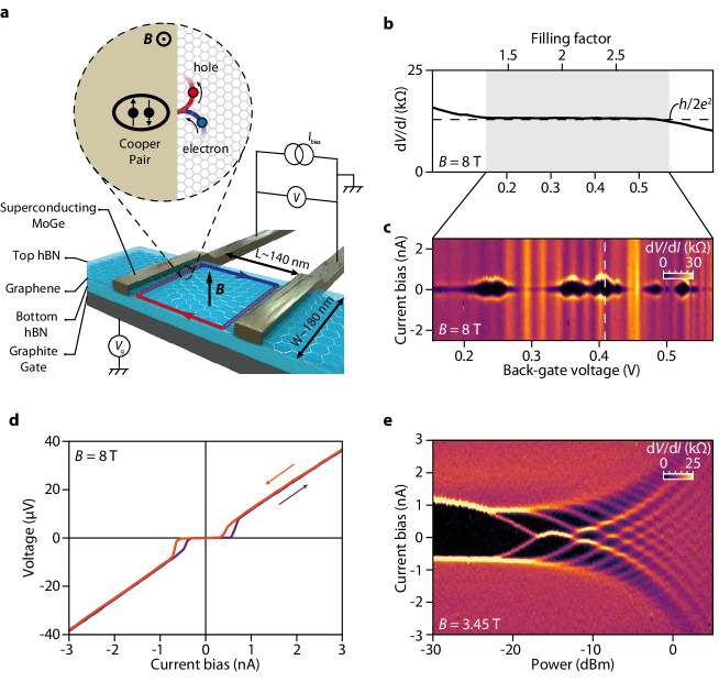
We fabricated QH-Josephson junctions with exfoliated graphene nanoribbons encapsulated between hexagonal boron-nitride flakes[40]. The resulting heterostructures lay atop exfoliated graphite flakes that serve as back-gate electrode to tune the charge carrier density with a voltage (Fig. 1a). We chose MoGe as superconducting contact material, with a high upper critical field ( T, see SI) and a contact resistance of m averaged from 13 devices. To ensure a good quantization of the QH plateau[41, 42], we designed junctions with aspect ratio , where is the width of the superconductor-graphene contact and the distance between the two contacts (see Extended Data Table 1). All measurements are performed at a temperature of K.
Supercurrent on quantum Hall plateau
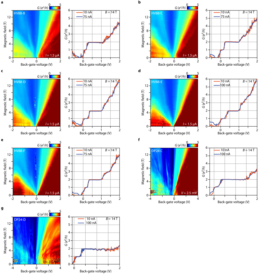
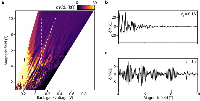
An essential benchmark for demonstrating superconducting transport through QH edge channels is the conjunction of a well-defined supercurrent and a QH plateau in the normal state. This is validated in Fig. 1b and c that display the two-terminal resistance as a function of back-gate voltage at T for a junction with nm and nm. Figure 1b displays the normal state resistance measured at a high current bias of A, which shows a well quantized plateau, indicating edge transport without bulk backscattering. Concomitantly, the differential resistance map at low current bias in Fig. 1c reveals pockets of supercurrent with zero resistance state color coded in black. Individual current-voltage characteristics (Fig. 1d) show a well-defined, hysteretic supercurrent with zero voltage drop below a switching current of nA.
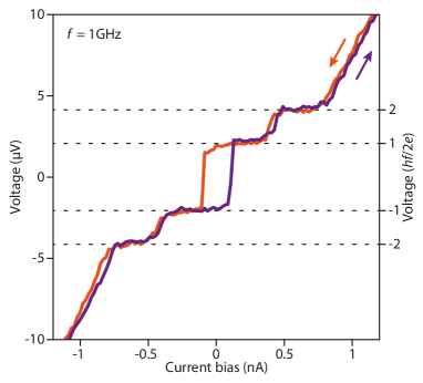
To get insight into the current-phase relation of the junction, we performed Shapiro steps measurements under irradiation by a microwave tone of frequency GHz. Fig. 1e displays a typical map of as a function of current bias and microwave power, measured on the QH plateau. As the microwave power is ramped up, Shapiro voltage steps develop and are visible as zero areas color coded in black. The height of these steps is (see Extended Data Fig. 6) in agreement with the theoretical expectation . This observation was reproduced at different frequencies (see SI), and indicates a conventional -periodic current-phase relation, as expected for the spin-degenerate QH edge channel at filling factor 2 (ref.[17, 19, 20]).
Quantum interference of chiral supercurrent
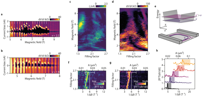
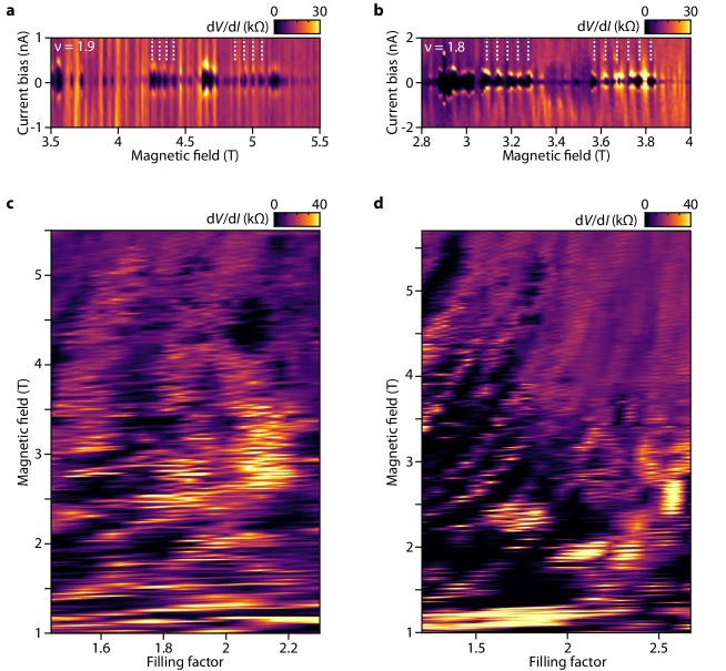
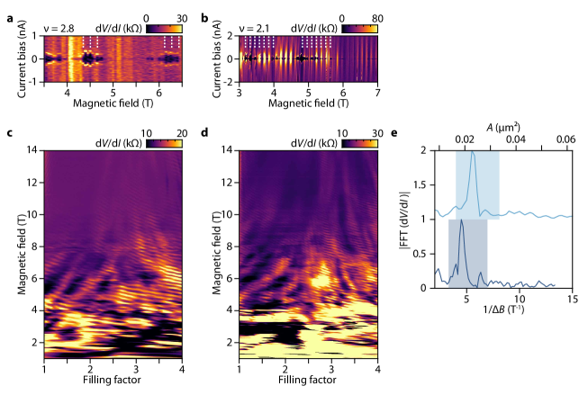
We now turn to the central result of this work, that is, demonstration of the distinct flux periodicity of the chiral supercurrent. Supercurrent oscillations are readily seen in Fig. 2a and b, which display two typical maps as a function of magnetic field and current bias, at filling factor and , respectively (see SI for the evaluation of ). At constant filling factor (non-constant back-gate voltage), superconducting pockets are observed over a large -range showing periodic oscillations. To evaluate the periodicity of the supercurrent oscillations, we superpose on Fig. 2a and b a comb of white dashed lines equally spaced by , that is, twice the superconducting flux quantum divided by the effective graphene area. Clearly, maxima of the supercurrent oscillation match the flux periodicity, the hallmark of the chiral supercurrent. Slight shifts of the oscillation are sometimes seen, such as for the last two white dashed lines above 7 T in Fig. 2b.
The key to this finding lies in analyzing the supercurrent oscillation at constant filling factor instead of fixed back-gate voltage. Indeed, for the latter, the charge carrier density is constant and the filling factor decreases with , leading to an inward displacement of the QH edge channels relative to the physical edge of the graphene flake and hence a decrease in the effective area. For our ultra-narrow junctions, such an area variation is sufficient to alter the flux periodicity (see SI Fig. S9). Conversely, at constant filling factor, that is, at constant Fermi level position in the cyclotron gap, the edge channel remains at a nearly -independent spatial position, enabling us to unveil the flux periodicity.
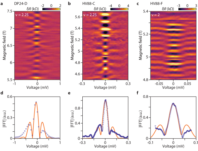
To substantiate our findings we present in Fig. 2c a full mapping of the supercurrent (see Methods) over the QH plateau. The -periodic supercurrent oscillations form fringes with negative slope, extending all over the plateau, on top of a slowly varying supercurrent background. Figure 2f shows a Fourier transform of these fringes performed at constant filling factor. The peak at , which indicates the period of the supercurrent oscillations, is close but slightly smaller than the value expected for -periodic oscillations related to the geometric graphene area (see white solid line and error bar related to the uncertainty in the nanoribbon width). This slightly smaller effective area can be accounted for by taking into account the distance between the actual edge state and the physical graphene edge, which is of the order of the magnetic length (see white dashed line). The close match between the periodicity and the corresponding geometric graphene area indicates that the QH edge channel is located in the immediate vicinity of the crystal edge, in agreement with recent scanning tunneling spectroscopy results[43].
In addition, one can notice a shift of the peak to higher frequency upon increasing . This shift reflects the increase in area with due to the slight displacement of the QH edge channel towards the graphene edge, as sketched in Fig. 2e, therefore providing a signature of the Landau level dispersion at the edge. From Fig. 2f, we obtain an area variation of m2, which corresponds to an edge channel displacement of nm, i.e. of the order of the magnetic length.
Importantly, the supercurrent oscillations are accompanied by resistance oscillations of the resistive state, as seen in Figs. 1c, 2a and 2b. The map at zero bias in Fig. 2d shows similar fringes with negative slope as for the critical current in Fig. 2c (both maps are extracted from the same set of data). The Fourier transform of the resistance oscillations (Fig. 2g) also reveals a flux periodicity with the same frequency shift with as the supercurrent. We ascribe these resistive state oscillations to a consequence of the Aharonov-Bohm phase picked by the charge carriers circulating around the QH channel loop, while undergoing chiral Andreev reflections along the superconducting interfaces. Note that, contrary to usual Josephson junctions, maxima of supercurrent do not necessarily coincide with minima of resistive state (see e.g. Fig. 2a and b). This is not surprising as the phase accumulated by CAES differs from that accumulated in the normal state by an additional phase shift picked up upon Andreev reflections.
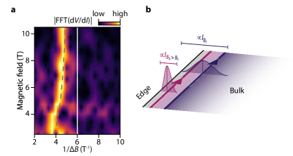
Inspecting Figs. 2c and d more closely, we see a decrease in the oscillation period with magnetic field, which translates to an increase in effective area. This variation can be accounted for by a decrease in the width of the Landau level wavefunction that scales as , which in turn results in the displacement of the QH edge channels towards the graphene edge (see Fig. 3b). Here, unlike Figs. 2f, g and e, the area variation is not related to the edge dispersion of the Landau level, but to the wavefunction shrinkage. An approximate correction of the flux area by the magnetic length , assuming a displacement of relative to the graphene edges, is shown as a grey dashed line in Fig. 3a. This correction is superimposed in Fig. 3a on the Fourier transform of Fig. 2d, which is computed here in a -window sliding along the -axis at fixed filling factor, and fits remarkably well the observed shift. Such a fine analysis of the area variation due to the wavefunction shrinkage with magnetic field confirms that the flux periodicity is observed over the whole range of magnetic field.
We obtained equivalent results for six other junctions for both critical current and resistive state oscillations (see SI). As a summary, we present in Fig. 2h the Fourier transforms of the oscillation for five junctions of different sizes, which show an excellent agreement with the expected flux periodicity indicated by colored rectangles. Such a systematic set of data therefore provides a conclusive demonstration of the flux periodicity of the chiral supercurrent.
Velocity renormalization at superconducting interface
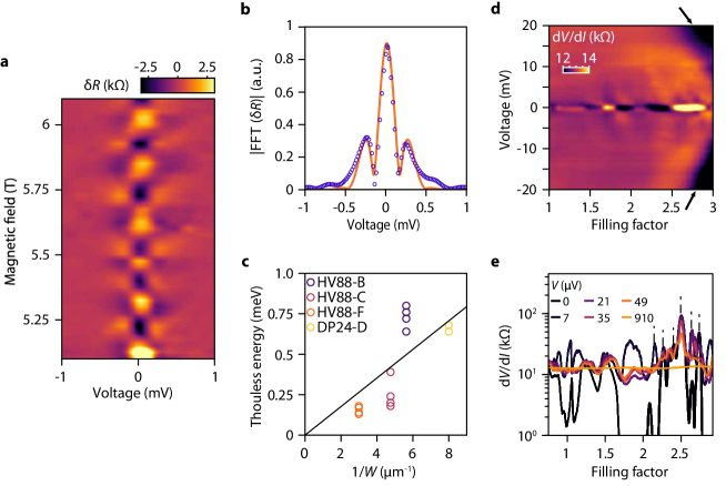
We now analyse the energy dependence of the resistance oscillations. Figure 4a shows as a function of the measured voltage across the junction and magnetic field at constant filling factor . The -periodic oscillations undergo a phase shift of at finite bias V, forming a checkerboard pattern resembling that of Fabry-Pérot QH interferometers[44, 45]. While latter contain a loop of QH edge channels partially transmitted through quantum point contacts, here the configuration is different since the quantum point contacts are replaced by superconducting interfaces, which are partially reflecting the QH edge states through Andreev processes with finite transparency. The checkerboard pattern thus results from the phase shift due to the finite energy of the injected electrons, where is the ballistic Thouless energy related to the traveling time along half of the loop perimeter. Following Ref.[44], we plot the Fourier transform of the checkerboard pattern in Fig. 4b and extract eV. Importantly, this value is smaller than what is expected for a QH edge state velocity ms measured in QH interferometers [44], which would give meV for the loop with half-perimeter nm. This estimate is instead consistent with the data at 14T above the critical field of the electrode shown in Extended Data Figure 5, in which we measured meV.
This discrepancy can be understood if we consider the CAES velocity renormalization along the superconducting interface[39, 21]. Due to the time delay of the Andreev process, that is, the extra time of the order of that an impinging electron spends in the electrode with a superconducting gap , the edge velocity along the superconducting interface drops significantly. As a result, and the Thouless energy is dominated by the interface width , , when . From the analysis of four junctions of different sizes (see other checkerboards in Extended Data Fig. 7), taken between 4.5 and 6 T, the evolution of with shown in Fig. 3c gives an estimate of ms, which is much smaller than . Theoretically, the edge state velocity renormalization for a non ideal interface can be derived from the Andreev bound states spectrum[39] (see Methods). From Eq. (2) in Methods, we obtain ms, whose order of magnitude is in good agreement with the experimental estimate. Interestingly, such a renormalization leads to a suppression of when vanishes at the upper critical field of the electrodes. This effect may be delicate to observe due to a crossover at to a regime where normal electrons take over the interference pattern.
The key parameter that limits the supercurrent in QH Josephson junctions at finite temperature is therefore the width of the superconducting interface, which severely reduces the Thouless energy via edge state velocity renormalization[39, 21]. This could provide an explanation for measurable supercurrent limited to small magnetic fields and high filling factors in the large junctions of Ref.[8]. In contrast, in the graphene nanoribbons studied here, a well-defined critical current withstands up to 8 T on the QH plateau. Furthermore, contrary to conventional Josephson junctions, increasing interface transparency further suppresses supercurrent by reducing (see Eq. (2) in Methods) and consequently the Thouless energy. Counter-intuitively, low transparency contacts may thus be a way to enhance critical current.
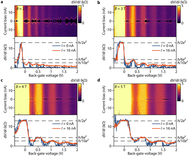
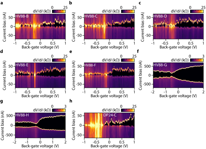
For consistency check, we studied wider junctions with to m and to nm on sample HV88 with similar contact transparencies (see HV88-G and HV88-H in SI Table S1). In these devices, the supercurrent is absent on QH plateaus and mostly visible at the transition between plateaus, where transport takes place through the bulk of the junction (see Extended Data Fig. 8). Note that other mechanisms involving decoherence due to disorder at the interface[22, 23] or vortices[46, 24] could be equally relevant and lead to the same conclusion, although more delicate to assess experimentally[16].
Inspecting the current-voltage characteristics at higher bias, we further observe signatures of CAES interference along the superconducting interface, which emerge as filling factor dependent resistance fluctuations[47, 48]. Figure 4d and e display the differential resistance fluctuations related to the background fluctuations of the switching current and resistance seen in Figs. 2b and d. Those are strongly suppressed above a voltage bias of about mV, which is close to as usually expected in standard hybrid Josephson junctions[49]. The fluctuation pattern echoes recent conductance fluctuations observed downstream superconducting interfaces[12], ascribed to CAES interference involving intervalley-scattering[50].
Interestingly, Fig. 4d reveals the breakdown of the QH plateau with a drop in resistance at high current bias near the transition to the next QH plateau (see black arrows). Although at this breakdown occurs here at relatively large bias with respect to superconducting features, the situation may be detrimental for other QH plateaus with small energy gaps as those of the fractional QH states. For these correlated states, the need to reduce the superconducting interface width to obtain a robust supercurrent should therefore meet another constraint related to edge transport, since QH breakdown critical current is significantly weakened in narrow structures.
Finally, we shall recall the spurious charging effects in Fabry-Pérot QH interferometers that have competed with and obscured the Aharonov-Bohm effect for some time[51]. It is therefore appropriate to examine the role of the Coulomb interaction in our small devices. As shown in Extended Data Figure 9, we observed Coulomb blockade signatures at the edges of the QH plateau and in the transition to the next plateau, in the regime where a compressible island should form in the bulk. However, the Coulomb blockade quickly disappears as soon as the QH plateau is entered to give way to Aharonov-Bohm interference. Furthermore, the slope of the interference fringes in the plane is negative, which is in agreement with Aharonov-Bohm dominated oscillations[51]. The distinct separation between Coulomb blockade signatures near the plateau transition and Aharonov-Bohm interference on the plateau, along with the negative fringes slope and correct area hence rule out charging effects in the -periodic oscillations.
Methods
Sample fabrication and parameters
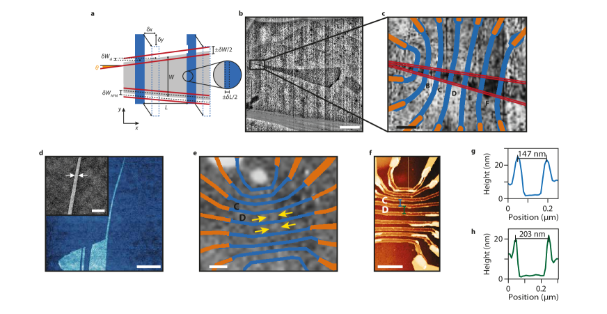
The graphene and hBN flakes used to fabricate the heterostructures were exfoliated and selected according to their surface cleanliness as determined by atomic force microscopy (AFM). AFM images were further used to locate the nanoribbons for subsequent lithography steps, and to measure the nanoribbon width at different positions with an accuracy of about 30 nm, as shown in Extended Data Fig. 1. Graphene/hBN heterostructures were assembled with the van der Waals pick-up technique[40] using a polycarbonate polymer. The heterostructures were deposited on a thin layer of graphite serving as a back-gate electrode. Large scale wiring (Ti/Au bilayer) and superconducting MoGe electrodes were patterned by two consecutive fabrication sequences including electron-beam lithography, metal deposition and liftoff. MoGe electrodes were deposited by DC-magnetron sputtering of a target, after etching of the stack with a CHF3/O2 plasma directly through the resist pattern used to define the contacts. The critical temperature of MoGe tested on a separate film is 5.9 K corresponding to a superconducting gap of eV. The upper critical field of the MoGe electrodes of the sample varies between 12.5 to 13 T (see Fig. S1). The geometrical parameters of the two samples studied in this work, HV88 and DP24, are reported in Extended Data Table 1. The top hBN, bottom hBN and graphite thicknesses are 12.7, 23.2 and 7.7 nm for HV88, and 25, 36 and 20 nm for DP24.
Each junction area is estimated from the superposition of the lithographic design with the AFM image of the heterostructure as illustrated in Extended Data Fig. 5, and confirmed with the AFM image of the device after contact fabrication (see Extended Data Fig. 5f-h). The precision on the flake width from the AFM image is estimated to be . The junction width uncertainty is dominated by this with negligible contribution from lithographic alignment uncertainty (). Indeed, a lithographic misalignment along the junction width direction, estimated to be smaller than 100 nm, has no effect on the junction width since the electrodes are parallel over more than 300 nanometers as shown in Extended Data Fig. 5a. The alignment precision of the superconducting electrodes with respect to the flake in the direction is estimated to be about nm. The resulting width uncertainty is given by with the nanoribbon opening angle as defined in Extended Data Fig. 5a. With and , the width uncertainty from alignment is about for HV88 and for DP24. The total uncertainty on the junction width is thus given by , hence for HV88 and for DP24. The uncertainty on the junction length originating from lithographic development and etching is estimated from dose test measurements to be about . The resulting uncertainty in the junction area is reported for all junctions in Extended Data Table 1.
.1 Measurements
Measurements were performed in a dilution refrigerator with a base temperature of K and equipped with a 14 T superconducting solenoid magnet. The sub nA switching current measurements (see Fig. 1) were resolved thanks to a heavily filtered wiring comprising feedthrough -filters (Tusonix #4209-053) at room temperature, custom-designed all stainless steel pico-coax cables (0.05 mm inner conductor diameter, 0.5 mm outer diameter), copper powder filters at the mixing chamber plate, and 47 nF (NPO dielectric[52]) capacitor to ground on the sample holder. characteristics were measured in a pseudo-four probe configuration as illustrated in Fig. 1a with an acquisition card (National Instruments NI-6346). The voltage drop across the junction was measured with a differential FET amplifier (DLPVA-100-F-D from FEMTO Messtechnik GmbH). Oversampling at 30 to 150 kHz per point with the acquisition card, along with very low level of low-frequency noise obtained by ground loop mitigation, enabled us to obtain well defined curves with an acquisition time of to s per curve. This fast acquisition enabled us to measure more than 30 000 curves in the plane to entirely map out the QH plateau and to observe the critical current and resistance oscillations. Differential resistance data were obtained by numerically differentiating characteristics. Only the resistance data of Fig. S13c and d were obtained by standard lockin amplifier technique. Shapiro maps were obtained with a microwave radiation source feeding a coaxial cable with the open end positioned about one millimeter above the devices.
.2 Edge state velocity renormalization
The energy spectrum of the Andreev bound states along a superconducting interface has been calculated by Hoppe et. al.[39]. For a non-ideal interface, it reads:
| (1) |
with the distance from the interface, the Landau level index, and is an oscillatory function of the filling factor. with the Fermi velocity mismatch between graphene and the superconductor and is the scattering at the interface corresponding to 2Z in the Blonder-Tinkham-Klapwijk model[53, 49]. While can be evaluated to be 1.4 (Fermi velocity is in MoGe[54], and in graphene), there is no experimental way to assess . However, using the expression of the transparency for a non-perfect superconductor-metal interface of Ref.[55], we can identify with . Then, the edge velocity is given by , which, with Eq. (1), leads to:
| (2) |
The contact transparency (see SI table S1) gives . With a superconducting critical temperature K for MoGe (see SI) corresponding a superconducting gap , we estimate at 5 T, with T (see SI). With at 5 T, we obtain .
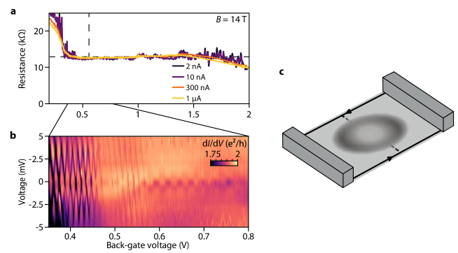
.3 Coulomb blockade at the plateau transition
The Coulomb blockade, an ubiquitous phenomenon in small mesoscopic systems, is found to occur at the transition between the plateaus. To illustrate this effect, we focus in Extended Data Fig. 9 on the left side of the plateau upon approaching the transition to plateau, at T, that is, above the critical field of the superconducting electrodes. A clear transition from the Fabry-Pérot checkerboard pattern, for V, to Coulomb diamonds, for V, occurs (see Extended Data Fig. 9b). Note that we have continuously observed -periodic resistance oscillations beyond the critical field of the electrode, but with much lower visibility and higher Thouless energy. Contrary to the orthodox picture, the Coulomb blockade leads to quantized conductance inside the diamond and a decrease in the conductance at resonance (see diamonds in Extended Data Fig. 9b delimited by darker conductance lines). Physically, as the back-gate voltage is decreased near the plateau transition, charge carriers are progressively removed from the zeroth Landau level, resulting in the emergence of a compressible island in the graphene bulk (see Extended Data Fig. 9c). As a result, this island, when tunnel-coupled to the QH edge channels on both sides of the sample, induces back-scattering at resonance, hence decreasing the QH conductance.
From the Coulomb diamonds in Extended Data Fig. 9b, we extract a charging energy of meV as well as an estimate of the diameter of the compressible island of nm, assuming it to be circular, which is a reasonable size for the dimension of the junction ( nm2). This, together with the remarkable regularity of the diamonds, confirm the picture of a single and large compressible island in the graphene bulk upon approaching the transition between plateaus.
Acknowledgments
We thank D. Basko, C. Beenakker, M. Feigel’Man, L. Glazman, M. Houzet, V. Kurilovich, J. Meyer, Y. Nazarov, K. Snizhko and A. Stern for valuable discussions. We thank F. Blondelle for technical support on the experimental apparatus. Samples were prepared at the Nanofab facility of the Néel Institute. This work has received funding from the European Union’s Horizon 2020 research and innovation program under the ERC grant SUPERGRAPH No. 866365. It also benefited from a French government grant managed by the ANR agency under the ’France 2030 plan’, with reference ANR-22-PETQ-0003. B.S., H.S. and W.Y. acknowledge support from the QuantERA II Program that has received funding from the European Union’s Horizon 2020 research and innovation program under Grant Agreement No 101017733. K.W. and T.T. acknowledge support from the JSPS KAKENHI (Grant Numbers 20H00354, 21H05233 and 23H02052) and World Premier International Research Center Initiative (WPI), MEXT, Japan.
References
- Stern and Lindner [2013] A. Stern and N. H. Lindner, Topological quantum computation–from basic concepts to first experiments, Science 339, 1179 (2013).
- Alicea and Stern [2015] J. Alicea and A. Stern, Designer non-Abelian anyon platforms: from Majorana to Fibonacci, Physica Scripta 2015, 014006 (2015).
- Alicea and Fendley [2016] J. Alicea and P. Fendley, Topological phases with parafermions: theory and blueprints, Annual Review of Condensed Matter Physics 7, 119 (2016).
- Rickhaus et al. [2012] P. Rickhaus, M. Weiss, L. Marot, and C. Schonenberger, Quantum Hall effect in graphene with superconducting electrodes, Nano letters 12, 1942 (2012).
- Komatsu et al. [2012] K. Komatsu, C. Li, S. Autier-Laurent, H. Bouchiat, and S. Guéron, Superconducting proximity effect in long superconductor/graphene/superconductor junctions: From specular Andreev reflection at zero field to the quantum Hall regime, Phys. Rev. B 86, 115412 (2012).
- Ben Shalom et al. [2016] M. Ben Shalom, M. J. Zhu, V. I. Fal’ko, A. Mishchenko, A. V. Kretinin, K. S. Novoselov, C. R. Woods, K. Watanabe, T. Taniguchi, A. K. Geim, and J. R. Prance, Quantum oscillations of the critical current and high-field superconducting proximity in ballistic graphene, Nature Physics 12, 318 (2016).
- Wan et al. [2015] Z. Wan, A. Kazakov, M. J. Manfra, L. N. Pfeiffer, K. W. West, and L. P. Rokhinson, Induced superconductivity in high-mobility two-dimensional electron gas in gallium arsenide heterostructures, Nature Communications 6, 7426 (2015).
- Amet et al. [2016] F. Amet, C. T. Ke, I. V. Borzenets, J. Wang, K. Watanabe, T. Taniguchi, R. S. Deacon, M. Yamamoto, Y. Bomze, S. Tarucha, and G. Finkelstein, Supercurrent in the quantum Hall regime, Science 352, 966 (2016).
- Lee et al. [2017] G.-H. Lee, K.-F. Huang, D. K. Efetov, D. S. Wei, S. Hart, T. Taniguchi, K. Watanabe, A. Yacoby, and P. Kim, Inducing superconducting correlation in quantum Hall edge states, Nature Physics 13, 693 (2017).
- Park et al. [2017] G.-H. Park, M. Kim, K. Watanabe, T. Taniguchi, and H.-J. Lee, Propagation of superconducting coherence via chiral quantum-Hall edge channels, Scientific Reports 7, 1 (2017).
- Seredinski et al. [2019] A. Seredinski, A. W. Draelos, E. G. Arnault, M.-T. Wei, H. Li, T. Fleming, K. Watanabe, T. Taniguchi, F. Amet, and G. Finkelstein, Quantum Hall-based superconducting interference device, Science Advances 5, eaaw8693 (2019).
- Zhao et al. [2020] L. Zhao, E. G. Arnault, A. Bondarev, A. Seredinski, T. F. Q. Larson, A. W. Draelos, H. Li, K. Watanabe, T. Taniguchi, F. Amet, H. U. Baranger, and G. Finkelstein, Interference of chiral Andreev edge states, Nature Physics 16, 862 (2020).
- Wang et al. [2021] D. Wang, E. J. Telford, A. Benyamini, J. Jesudasan, P. Raychaudhuri, K. Watanabe, T. Taniguchi, J. Hone, C. R. Dean, and A. N. Pasupathy, Andreev Reflections in NbN/Graphene Junctions under Large Magnetic Fields, Nano Letters 21, 8229 (2021).
- Gül et al. [2022] Ö. Gül, Y. Ronen, S. Y. Lee, H. Shapourian, J. Zauberman, L. Y. H., K. Watanabe, T. Taniguchi, A. Vishwanath, A. Yacoby, and P. Kim, Andreev reflection in the fractional quantum Hall state, Physical Review X 12, 021057 (2022).
- Hatefipour et al. [2022] M. Hatefipour, J. J. Cuozzo, J. Kanter, W. M. Strickland, C. R. Allemang, T.-M. Lu, E. Rossi, and J. Shabani, Induced Superconducting Pairing in Integer Quantum Hall Edge States, Nano Letters 22, 6173 (2022).
- Zhao et al. [2022] L. Zhao, Z. Iftikhar, T. F. Larson, E. G. Arnault, K. Watanabe, T. Taniguchi, F. Amet, and G. Finkelstein, Loss and decoherence at the quantum Hall - superconductor interface, arXiv:2210.04842 (2022).
- Ma and Zyuzin [1993] M. Ma and A. Y. Zyuzin, Josephson effect in the quantum hall regime, Europhysics Letters 21, 941 (1993).
- Zyuzin [1994] A. Y. Zyuzin, Superconductor–normal-metal–superconductor junction in a strong magnetic field, Phys. Rev. B 50, 323 (1994).
- Stone and Lin [2011] M. Stone and Y. Lin, Josephson currents in quantum Hall devices, Physical Review B 83, 224501 (2011).
- Van Ostaay et al. [2011] J. A. M. Van Ostaay, A. R. Akhmerov, and C. W. J. Beenakker, Spin-triplet supercurrent carried by quantum Hall edge states through a Josephson junction, Physical Review B 83, 195441 (2011).
- Alavirad et al. [2018] Y. Alavirad, J. Lee, Z.-X. Lin, and J. D. Sau, Chiral supercurrent through a quantum Hall weak link, Physical Review B 98, 214504 (2018).
- Manesco et al. [2022a] A. L. R. Manesco, I. M. Flór, C.-X. Liu, and A. R. Akhmerov, Mechanisms of Andreev reflection in quantum Hall graphene, SciPost Phys. Core 5, 045 (2022a).
- Kurilovich et al. [2022] V. D. Kurilovich, Z. M. Raines, and L. I. Glazman, Disorder in Andreev reflection of a quantum Hall edge, arXiv:2201.00273 (2022).
- Tang et al. [2022] Y. Tang, C. Knapp, and J. Alicea, Vortex-enabled Andreev processes in quantum Hall–superconductor hybrids, Phys. Rev. B 106, 245411 (2022).
- Qi et al. [2010] X. L. Qi, T. L. Hughes, and S. C. Zhang, Chiral topological superconductor from the quantum Hall state, Physical Review B 82, 184516 (2010).
- Clarke et al. [2012] D. J. Clarke, J. Alicea, and K. Shtengel, Exotic non-Abelian anyons from conventional fractional quantum Hall states, Nature Communications 4, 1348 (2012).
- Lindner et al. [2012] N. H. Lindner, E. Berg, G. Refael, and A. Stern, Fractionalizing majorana fermions: Non-abelian statistics on the edges of abelian quantum hall states, Physical Review X 2, 041002 (2012).
- Vaezi [2013] A. Vaezi, Fractional topological superconductor with fractionalized Majorana fermions, Phys. Rev. B 87, 035132 (2013).
- Clarke et al. [2014] D. J. Clarke, J. Alicea, and K. Shtengel, Exotic circuit elements from zero-modes in hybrid superconductor–quantum-Hall systems, Nature Physics 10, 877 (2014).
- Mong et al. [2014] R. S. K. Mong, D. J. Clarke, J. Alicea, N. H. Lindner, P. Fendley, C. Nayak, Y. Oreg, A. Stern, E. Berg, K. Shtengel, and M. P. A. Fisher, Universal topological quantum computation from a superconductor-abelian quantum hall heterostructure, Physical Review X 4, 011036 (2014).
- Beenakker [2014] C. W. J. Beenakker, Annihilation of Colliding Bogoliubov Quasiparticles Reveals their Majorana Nature, Phys. Rev. Lett. 112, 070604 (2014).
- San-Jose et al. [2015] P. San-Jose, J. L. Lado, R. Aguado, F. Guinea, and J. Fernández-Rossier, Majorana Zero Modes in Graphene, Phys. Rev. X 5, 041042 (2015).
- Finocchiaro et al. [2018] F. Finocchiaro, F. Guinea, and P. San-Jose, Topological junctions from crossed andreev reflection in the quantum hall regime, Phys. Rev. Lett. 120, 116801 (2018).
- Snizhko et al. [2018] K. Snizhko, R. Egger, and Y. Gefen, Measurement and control of a Coulomb-blockaded parafermion box, Phys. Rev. B 97, 081405 (2018).
- Nielsen et al. [2022] I. E. Nielsen, K. Flensberg, R. Egger, and M. Burrello, Readout of parafermionic states by transport measurements, Phys. Rev. Lett. 129, 037703 (2022).
- Galambos et al. [2022] T. H. Galambos, F. Ronetti, B. Hetényi, D. Loss, and J. Klinovaja, Crossed Andreev reflection in spin-polarized chiral edge states due to the Meissner effect, Phys. Rev. B 106, 075410 (2022).
- Nayak et al. [2008] C. Nayak, S. H. Simon, A. Stern, M. Freedman, and S. Das Sarma, Non-Abelian anyons and topological quantum computation, Reviews of Modern Physics 80, 1083 (2008).
- Takagaki [1998] Y. Takagaki, Transport properties of semiconductor-superconductor junctions in quantizing magnetic fields, Phys. Rev. B 57, 4009 (1998).
- Hoppe et al. [2000] H. Hoppe, U. Zülicke, and G. Schön, Andreev reflection in strong magnetic fields, Physical Review Letters 84, 1804 (2000).
- Wang et al. [2013] L. Wang, I. Meric, P. Y. Huang, Q. Gao, Y. Gao, H. Tran, T. Taniguchi, K. Watanabe, L. M. Campos, D. A. Muller, J. Guo, P. Kim, J. Hone, K. L. Shepard, and C. R. Dean, One-Dimensional Electrical Contact to a Two-Dimensional Material, Science 342, 614 (2013).
- Abanin and Levitov [2008] D. A. Abanin and L. S. Levitov, Conformal invariance and shape-dependent conductance of graphene samples, Physical Review B 78, 035416 (2008).
- Williams et al. [2009] J. R. Williams, D. A. Abanin, L. Dicarlo, L. S. Levitov, and C. M. Marcus, Quantum Hall conductance of two-terminal graphene devices, Physical Review B 80, 045408 (2009).
- Coissard et al. [2022] A. Coissard, A. G. Grushin, C. Repellin, L. Veyrat, K. Watanabe, T. Taniguchi, F. Gay, H. Courtois, H. Sellier, and B. Sacépé, Absence of edge reconstruction for quantum Hall edge channels in graphene devices, arXiv:2210.08152 (2022).
- Déprez et al. [2021] C. Déprez, L. Veyrat, H. Vignaud, G. Nayak, K. Watanabe, T. Taniguchi, F. Gay, H. Sellier, and B. Sacépé, A tunable Fabry–Pérot quantum Hall interferometer in graphene, Nature Nanotechnology 16, 555 (2021).
- Ronen et al. [2021] Y. Ronen, T. Werkmeister, D. Haie Najafabadi, A. T. Pierce, L. E. Anderson, Y. J. Shin, S. Y. Lee, Y. H. Lee, B. Johnson, K. Watanabe, T. Taniguchi, A. Yacoby, and P. Kim, Aharonov–Bohm effect in graphene-based Fabry–Pérot quantum Hall interferometers, Nature Nanotechnology 16, 563 (2021).
- Kurilovich and Glazman [2022] V. D. Kurilovich and L. I. Glazman, Criticality in the crossed Andreev reflection of a quantum Hall edge, arXiv:2209.12932 (2022).
- Chtchelkatchev and Burmistrov [2007] N. M. Chtchelkatchev and I. S. Burmistrov, Conductance oscillations with magnetic field of a two-dimensional electron gas-superconductor junction, Physical Review B 75, 214510 (2007).
- Batov et al. [2009] I. Batov, T. Schaepers, N. Chtchelkatchev, A. Golubov, H. Hardtdegen, and A. Ustinov, Electronic transport in mesoscopic superconductor/2D electron gas junctions in strong magnetic field, Bulletin of the Russian Academy of Sciences: Physics 73, 880 (2009).
- Blonder et al. [1982] G. E. Blonder, M. Tinkham, and T. M. Klapwijk, Transition from metallic to tunneling regimes in superconducting microconstrictions: Excess current, charge imbalance, and supercurrent conversion, Phys. Rev. B 25, 4515 (1982).
- Manesco et al. [2022b] A. Manesco, I. M. Flór, C.-X. Liu, and A. Akhmerov, Mechanisms of Andreev reflection in quantum Hall graphene, SciPost Physics Core 5, 045 (2022b).
- Halperin et al. [2011] B. I. Halperin, A. Stern, I. Neder, and B. Rosenow, Theory of the Fabry-Pérot quantum Hall interferometer, Physical Review B 83, 155440 (2011).
- Teyssandier and Prêle [2010] F. Teyssandier and D. Prêle, Commercially available capacitors at cryogenic temperatures, Ninth International Workshop on Low Temperature Electronics-WOLTE9, https://hal.science/hal-00623399 (2010).
- Zülicke et al. [2001] U. Zülicke, H. Hoppe, and G. Schön, Andreev reflection at superconductor-semiconductor interfaces in high magnetic fields, Physica B: Condensed Matter 298, 453 (2001).
- Kim et al. [2018] H. Kim, F. Gay, A. Del Maestro, B. Sacépé, and A. Rogachev, Pair-breaking quantum phase transition in superconducting nanowires, Nature Physics 14, 912 (2018).
- Mazin et al. [1995] I. I. Mazin, A. A. Golubov, and A. D. Zaikin, “Chain Scenario” for Josephson Tunneling with Shift in YBC, Phys. Rev. Lett. 75, 2574 (1995).
- Calado et al. [2015] V. E. Calado, S. Goswami, G. Nanda, M. Diez, A. R. Akhmerov, K. Watanabe, T. Taniguchi, T. M. Klapwijk, and L. M. K. Vandersypen, Ballistic Josephson junctions in edge-contacted graphene, Nature Nanotechnology 10, 761 (2015).
- Allen et al. [2017] M. T. Allen, O. Shtanko, I. C. Fulga, J. I. Wang, D. Nurgaliev, K. Watanabe, T. Taniguchi, A. R. Akhmerov, P. Jarillo-Herrero, L. S. Levitov, and A. Yacoby, Observation of Electron Coherence and Fabry-Pérot Standing Waves at a Graphene Edge, Nano Letters 17, 7380 (2017).
- Octavio et al. [1983] M. Octavio, M. Tinkham, G. E. Blonder, and T. M. Klapwijk, Subharmonic energy-gap structure in superconducting constrictions, Phys. Rev. B 27, 6739 (1983).
- Büttiker [1988] M. Büttiker, Absence of backscattering in the quantum Hall effect in multiprobe conductors, Phys. Rev. B 38, 9375 (1988).
- Hong et al. [2020] S. Hong, C.-S. Lee, M.-H. Lee, Y. Lee, K. Y. Ma, G. Kim, S. I. Yoon, K. Ihm, K.-J. Kim, T. J. Shin, S. W. Kim, E.-c. Jeon, H. Jeon, J.-Y. Kim, H.-I. Lee, Z. Lee, A. Antidormi, S. Roche, M. Chhowalla, H.-J. Shin, and H. S. Shin, Ultralow-dielectric-constant amorphous boron nitride, Nature 582, 511 (2020).
- Flensberg et al. [1988] K. Flensberg, J. B. Hansen, and M. Octavio, Subharmonic energy-gap structure in superconducting weak links, Phys. Rev. B 38, 8707 (1988).
- Niebler et al. [2009] G. Niebler, G. Cuniberti, and T. Novotný, Analytical calculation of the excess current in the Octavio-Tinkham-Blonder-Klapwijk theory, Superconductor Science and Technology 22, 10.1088/0953-2048/22/8/085016 (2009).
- Chiodi et al. [2012] F. Chiodi, M. Ferrier, S. Guéron, J. C. Cuevas, G. Montambaux, F. Fortuna, A. Kasumov, and H. Bouchiat, Geometry-related magnetic interference patterns in long Josephson junctions, Phys. Rev. B 86, 064510 (2012).
- Tinkham [1996] M. Tinkham, Introduction to superconductivity (Dover, Mineola, 1996).
| Device | (nm) | (nm) | ||
|---|---|---|---|---|
| HV88-B | 140 | 178 | 1.27 | |
| HV88-C | 170 | 210 | 1.39 | |
| HV88-D | 200 | 247 | 1.43 | |
| HV88-E | 240 | 288 | 1.14 | |
| HV88-F | 270 | 334 | 1.55 | |
| HV88-G | 107 | 2332 | 2.12 | |
| HV88-H | 202 | 2434 | 1.93 | |
| DP24-C | 170 | 125 | 1.12 | |
| DP24-D | 200 | 125 | 1.89 |
Supplementary Information
I Critical temperature and upper critical field of the MoGe electrodes
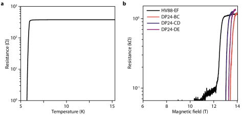
We present in this section the superconducting properties of the MoGe electrodes. We measured a superconducting transition temperature of K on a separate bare MoGe film (see Fig. S1a.) deposited in the same conditions as the electrodes of the samples. Transitions to normal state with magnetic field for some MoGe electrodes of both samples HV88 and DP24 are shown in Fig. S1b. The resistance was measured in a two-terminal configuration with a lock-in amplifier technique, at a temperature of 0.05 K. A constant resistance of 1.06 was subtracted to account for the wiring resistance in series with the electrodes. We measured a critical field of about 12.5 T for HV88 and 13.5 T for DP24.
II Device characterization
Here, we present the characterization of all devices, including their normal state properties at 6 K, the quantum Hall regime, and the Josephson junctions properties at zero and low magnetic field.
II.1 Graphene nanoribbon devices
Figure S2 displays the resistance versus back-gate voltage measured at a temperature of 6 K for HV88 and 4 K for DP24. The high value of resistance results mainly from the contact resistance, which is high due to the very narrow width of the contacts. The charge neutrality points of the devices are located at low negative back-gate voltage, indicating a residual electron-type doping. The higher value of the resistance for negative back-gate voltage is characteristic of charge transfer from the contacts, which induces an electron doping and thus a bipolar npn regime with reduced transparency. This bipolar npn regime is consistent with the resistance fluctuations seen in all junctions, which we ascribe to the Fabry-Pérot interferences between the pn interfaces routinely observed in high mobility devices [56, 6, 57]. The electron doping from the MoGe electrodes also explains why the quantum Hall effect is not well defined on the hole side (negative back-gate voltage), as shown in section II.2.
II.2 Quantum Hall effect in the graphene nanoribbons
The quantum Hall effect was characterized with a dc current bias of for HV88 at 10 mK and with a dc voltage bias of for DP24 at 4 K, to prevent deviation from quantization due to sub-gap features [58]. The resistance maps of the different junctions as a function of back-gate voltage and magnetic field are shown in Fig. S3. As discussed in the previous section, the hole side is badly quantized due to the npn bipolar regime. On the electron side, the quantum Hall plateau is well quantized from low magnetic field (from T depending on the device for narrow junctions). The visibility of other QH plateaus with smaller energy gap, as for instance the state, requires that the critical current for their QH breakdown is larger than the non-linearities induced by the Andreev reflections at finite bias (typically up to ). As a result, the state emerges as a well quantized plateau from T. It is clearly visible in the line-cuts taken at T in Fig. S3. Plateaus for filling factors meet the same issues. Their absence can furthermore be accounted for by a lack of equilibration between the edge channel of the zeroth Landau level and the edge channels of the higher Landau levels in our mesoscopic devices [59].
The line-cuts of Fig. S3 measured with a small current excitation at 14 T, that is, above the upper critical field of the electrodes are not altered by superconducting sub-gap features nor quantum Hall breakdown. We can see in Fig. S3e and d the emergence of the and 4 broken-symmetry states.
II.3 Back-gate capacitance estimation
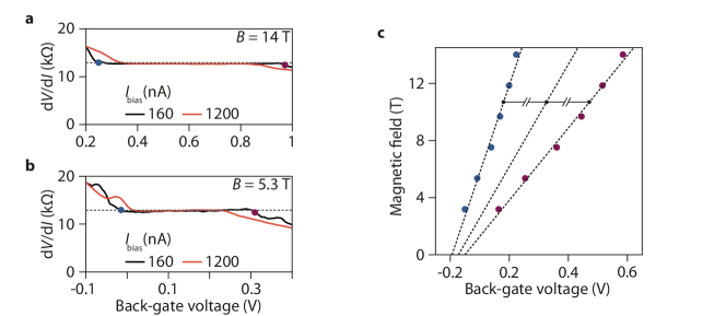
The quantum Hall data of Fig. S3 are used to quantify the back-gate capacitance. While a two-plate capacitor model gives for sample HV88 and for sample DP24 using a dielectric constant of for boron nitride [60], in very small structure the capacitance can be modified due to screening by the electrodes. We thus estimated the back-gate capacitance through the dispersion of the filling factor 2 plateau as shown in Fig. S4. The middle of the plateau is defined as . The curve at 160 nA is chosen as a reference to detect the plateau edges as it shows limited deviation from quantization compared to both lower and higher currents. These deviations originate from the non-linearities of the superconducting interface at low current, and from the quantum Hall breakdown at high current. The resulting capacitances that we used to calculate the filling factor are reported in the Extended Data Table I.
II.4 Contact resistance
If one assume ballistic transport within the junction, we can estimate the graphene resistance in the pure quantum limit [6]: , where account for the spin and valley degeneracies, respectively, and N is the number of transverse modes propagating in the graphene . and the electron density is defined as .
The difference between the measured resistance and provides the contact resistance . At V, we obtain averaged over 13 devices for the MoGe contacts. This corresponds to an average transmission probability . This transmission probability is half that obtained from the IV curves in the superconducting state (see section II.E). Note that a similar, though less pronounced, difference was observed in [6].
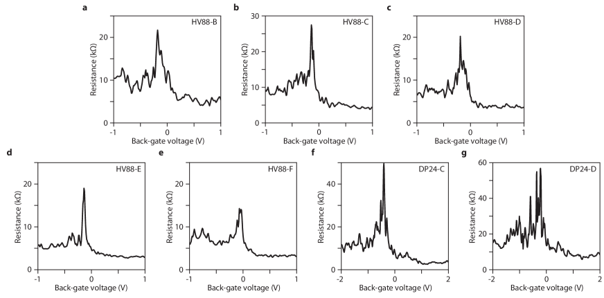
II.5 Supercurrent characterization at T
Figure S5 displays the differential resistance as a function of dc current bias and back-gate voltage at zero magnetic field for all devices. The decrease of resistance with back-gate voltage leads to an increase of switching current as expected for a constant product, where is the normal state resistance. We obtained ranging from V to V.
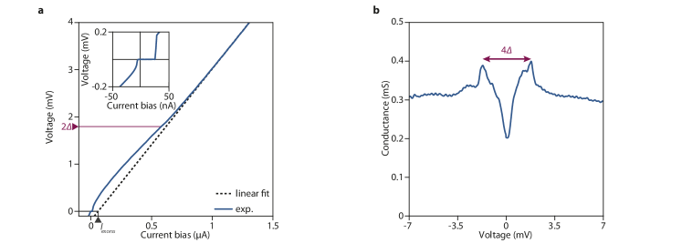
We estimated the contact transparency from characteristics following Ref. [58, 61, 62]. The normal state resistance is estimated from a linear fit at high current bias (see Fig.S6), and the excess current is defined as the intercept of this fit at zero voltage. The conductance plotted as a function of measured voltage exhibits two maxima, symmetric with respect to zero voltage, that we ascribe to twice the superconducting gap . Eq. (25) in Ref. [62] is used to deduce the Blonder-Tinkham-Klapwijk parameter , which leads to the transparency defined as . The transparency of our junctions are reported in Table 2 for 7 junctions, along with , , and .
| Junction | (V) | (V) | (nA) | () | () | |||
| HV88-C | -0.13 | -0.14 | 1 | 852 | 49 | 4.5 | 0.49 | 150 |
| HV88-D | -0.19 | -0.15 | 1 | 865 | 46 | 3.8 | 0.47 | 91 |
| HV88-E | -0.14 | -0.25 | 1 | 876 | 86 | 3.0 | 0.5 | 96 |
| HV88-F | -0.04 | -0.08 | 1 | 897 | 59 | 3.2 | 0.47 | 87 |
| HV88-G | -0.52 | -0.24 | 2 | 762 | 552 | 0.34 | 0.48 | 146 |
| HV88-H | -0.34 | -0.23 | 2 | 773 | 434 | 0.34 | 0.47 | 137 |
| DP24-C | -0.4 | -0.12 | 1 | 754 | 83 | 4.2 | 0.56 | 243 |
II.6 Fraunhofer patterns
In this section we present the quantum interference (Fraunhofer) patterns of the Josephson junctions at low magnetic field. Figure S7 displays the differential resistance as a function of current bias and magnetic field for 6 devices. The evolutions of the switching current do not follow the usual Fraunhofer pattern with a sinus cardinal decay. This is not clearly understood but we cannot exclude vortices trapped in the superconducting electrodes due to the relatively large field needed for reaching a flux quantum through the small graphene area of the junctions (e.g. mT for device HV88-B), as well as deviation from the Fraunhofer pattern due to the square geometry of the graphene [63]. Still, we can extract a flux period from the central lobs of these quantum interference patterns. The magnetic field at which the switching current vanishes for the central lob corresponds theoretically to [64]. We thus added white dashed lines in Fig. S7 that indicates the equivalent magnetic field for one flux quantum through the graphene area. We obtain a remarkably good agreement for all devices. Interestingly, Fraunhofer patterns nearly matching the graphene area have been observed in similar devices with square geometry () in [56].
III Additional Shapiro maps
We show in this section additional Shapiro maps, complementing the data of Fig. 1e. Figure S8 displays the Shapiro maps of the differential resistance along with characteristics measured with the same parameters of magnetic field and back-gate voltage as in Fig. 1e but with microwave frequencies of 3 GHz, in Fig. S8a and c, and at 6 GHz in Fig. S8b and d.

IV -periodic oscillations
IV.1 Constant back-gate voltage versus constant filling factor
In this section we illustrate the relevance of studying the flux periodicity of the supercurrent and resistance oscillations at constant filling factor compared to constant back-gate voltage. Figure S9 displays the zero bias differential resistance of sample HV88-D as a function of back-gate voltage and magnetic field. The measurement is restricted to the QH plateau to limit the the data acquisition to a reasonable duration. Fringes similar to that of Fig. 2d are visible in this resistance map. However, extracting a line-cut at constant back-gate voltage (along the vertical dashed line at V) does not exhibit any oscillatory behavior, as shown in Fig. S9b. On the other hand, a line-cut at constant filling factor (along the diagonal dashed line at ) shown in Fig. S9c clearly unveils the -periodic oscillations.
IV.2 Switching current and resistance oscillations on additional devices
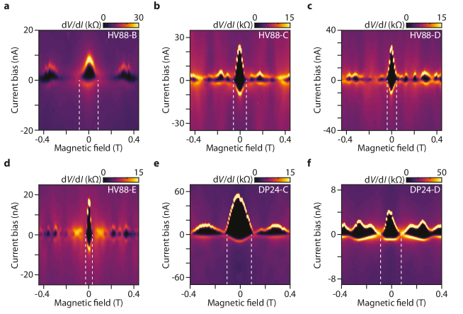
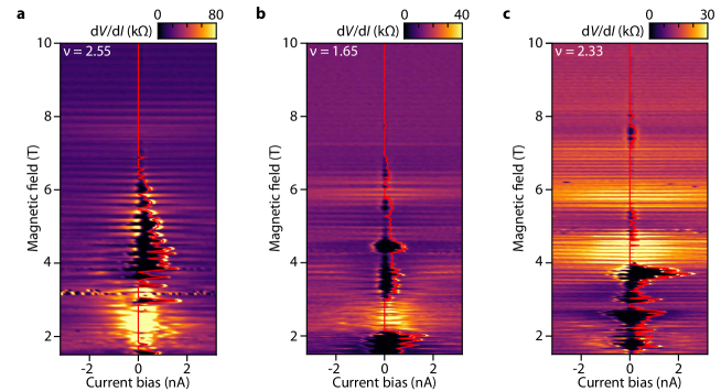
We show in Fig. S10 additional measurements of the -periodic oscillations of the supercurrent for the junctions HV88-B, HV88-C and HV88-D. The differential resistance map is plotted as a function of dc current bias and magnetic field, at constant filling factor. The red traces superimposed on each Figures show the detected switching current. Note that such a detection was used for the switching current map in Fig 2c for HV88-B.
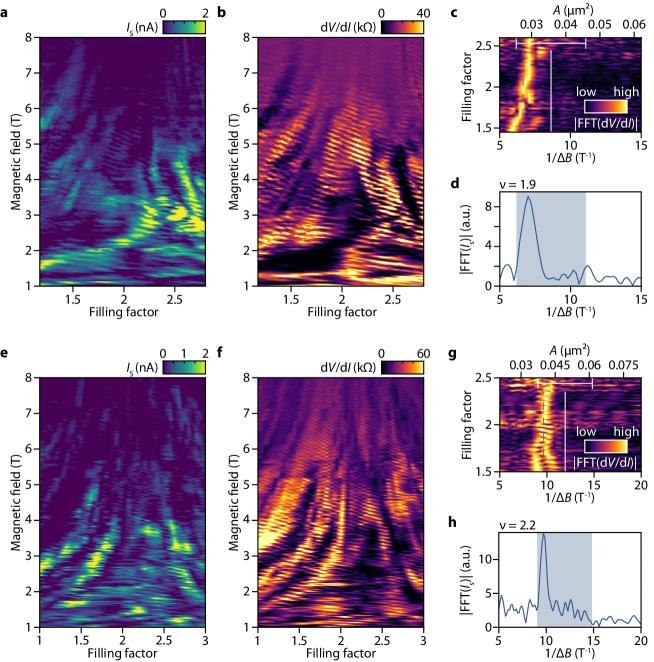
In Fig. S11 we show the switching current map and the zero bias resistance as a function of filling factor and magnetic field for the junctions HV88-C and HV88-D. Fig. S11c and g display the Fourier transform of the resistance map as a function of frequency and filling factor for HV88-C and HV88-D, respectively. Fig. S11d and h display the Fourier transform of the critical current oscillations as a function of frequency for HV88-C and HV88-D, respectively. The frequencies of these oscillations are in excellent agreement with the graphene area corrected by the magnetic length, therefore confirming the results presented in the main text.
The data of the two longest and widest nanoribbons, HV88-E, HV88-F, are shown in Fig. S12. Despite a smaller magnetic field period, we resolve the supercurrent and resistance oscillations on the QH plateau. Differential resistance maps as a function of magnetic field and current bias at fixed filling factors in Fig. S12a and b clearly show the -periodic oscillations of the supercurrent and of the resistance, as indicated by the white dashed lines. Similar results have been obtained on junctions DP24-C and DP24-D, as shown in Fig. S13.
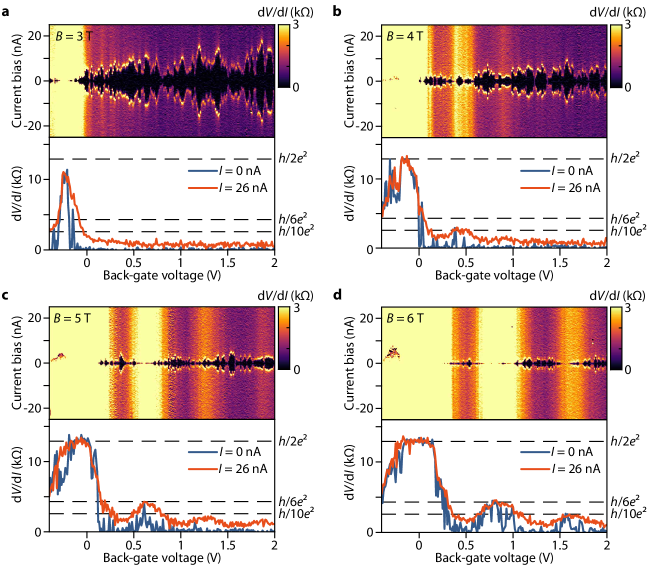
V Additional wide junction
We present in this section the data for a second wide junction (HV88-H) in complement to Extended Data Fig. 4. This junction has nearly the same width (m) but is twice longer than junction HV88-G. Figure S14 displays the differential resistance as a function of back-gate voltage and dc current bias at different magnetic field values, along with the differential resistance measured at 0 and 26 nA to show the superconducting pocket and the resistive state. As in Extended Data Fig. 4, supercurrent is conspicuously absent on the QH plateau. For low magnetic field there is a finite supercurrent in the QH plateau. However, this supercurrent vanishes when the resistance becomes quantized upon increasing magnetic field, indicating that this junction cannot maintain supercurrent in the edge transport regime. This is consistent with the suppression of the Thouless energy by the long superconducting interfaces, which in turn suppress the supercurrent [21].