Origin and stability of the charge density wave in ScV6Sn6
Abstract
Kagomé metals are widely recognized as versatile platforms for exploring novel topological properties, unconventional electronic correlations, magnetic frustration, and superconductivity. In the V6Sn6 family of materials ( = Sc, Y, Lu), ScV6Sn6 hosts an unusual charge density wave ground state as well as structural similarities with the V3Sb5 system ( = K, Cs, Rb). In this work, we combine Raman scattering spectroscopy with first-principles lattice dynamics calculations to reveal the charge density wave state in ScV6Sn6. In the low temperature phase, we find a five-fold splitting of the V-containing totally symmetric mode near 240 cm-1 suggesting that the density wave acts to mix modes of 6/ and symmetry - an effect that we quantify by projecting phonons of the high symmetry state onto those of the lower symmetry structure. We also test the stability of the density wave state under compression and find that both physical and chemical pressure act to quench the effect. We discuss these findings in terms of symmetry and the structure-property trends that can be unraveled in this system.
Introduction
Kagomé materials possess two-dimensional periodic networks of corner-sharing triangles and, as a result, exhibit a high degree of geometrical frustration. This structural frustration can create Dirac cones and flat bands in the electronic band structure, as well as exotic magnetic ground states 1; 2; 3; 4; 5; 6; 7; 8 accompanied by the anomalous Hall effect, 9; 10; 11; 12 charge fractionalization,13; 14 chiral magnetism, 15; 16 and strong electron correlations.17 The discovery of charge density waves (CDWs) in superconducting V3Sb5 ( = K, Rb, Cs) and magnetic FeGe demonstrates that CDWs can exist in both magnetic and nonmagnetic kagomé lattices across a range of electron correlations. 18; 19; 20 At the same time, rich phase diagrams can be obtained by tuning the frustration and electron filling in the kagomé lattice. Strong entanglements make this platform well-suited to revealing intertwined and competing states. Recently, a family of bi-layer analogs with chemical formula V6Sn6 ( = Sc, Y, Lu, Tb, Ho, Gd…) has attracted attention [Fig. 1a].21 These kagomé metals also host topological Dirac surface states, van Hove singularies, anisotropic magnetism, and other exciting properties.22; 23 That said, unlike all three V3Sb5 compounds, superconductivity has not been reported in ScV6Sn6 under any temperature or pressure conditions investigated thus far, 24; 25 possibly due to the lack of a -centered Fermi pocket in this material. 26; 27; 28; 29 Also, remarkably, only ScV6Sn6 exhibits a three dimensional CDW, making it comparable to the V3Sb5’s. Despite recent activity in this highly contemporary research area, there is much more to learn about the CDW in ScV6Sn6 and related materials. In particular, the combination of two kagomé layers per unit cell, along with the lower symmetry wavevector of the CDW makes resolving structural details and phase transition of ScV6Sn6 a particularly daunting task.
ScV6Sn6 is a paramagnetic metal with a first-order CDW transition at 92 K ().30; 25; 31; 32 The CDW primarily involves out-of-plane Sc and Sn displacements; thus far, the contribution of V centers has been neglected.25; 33 First-principles calculations point to lattice instabilities (soft modes) in ScV6Sn633 - possibly due to the small size of the Sc3+ radius. Experimentally, a phonon mode leads to short range order in the high temperature phase with wavevector (1/3, 1/3, 1/2). A stable long range CDW order with wavevector (1/3, 1/3, 1/3) sets in below 92 K in the low temperature phase.31; 32 This type of lattice instability is not present in the Y and Lu analogs, and there are no CDWs in these materials.33 Experimental confirmation of these predictions by other probes is highly desirable. Traditionally, x-ray techniques and vibrational spectroscopy have been favored for unraveling these issues. Infrared and Raman scattering spectroscopies in particular are well-suited for exploring the microscopic aspects of local lattice distortions as well as phase and amplitude modes of a CDW. Of course, the metallic character of ScV6Sn6 challenges this approach because the odd-symmetry infrared-active phonons are screened by the Drude contribution.34 Raman scattering provides a way forward,35 and it has been used to gain significant insight about the CDW in other kagomé systems36; 37 even though it accesses only even-symmetry features at the zone center. Compared to the AV3Sb5 family, Raman spectroscopy can provide more information about ScV6Sn6 because of the larger number of Raman active lattice modes in its crystal structure.
In this work, we combine temperature- and pressure-dependent Raman scattering spectroscopy of ScV6Sn6 with complementary lattice dynamics calculations to reveal the properties of the charge density wave states in this model bi-layer kagomé metal. What distinguishes our work from prior efforts38 is the quality of our single crystals with different site substitutions, the ability to employ both temperature and pressure as tuning parameters, and our symmetry-guided strategy of projecting the high temperature phase 6/ phonons onto those in the low temperature CDW state to uncover their origins. We find that the symmetry mode near 240 cm-1 - which involves out-of-plane V center motion - is very sensitive to the development of the CDW. For instance, even though it corresponds to a nondegenerate phonon mode, it seemingly displays five-fold splitting in the low temperature phase consistent with symmetry. We discuss this symmetry breaking in terms of mixing of nearby symmetry-appropriate and zone-folded phonons. We also demonstrate that compression at room temperature quenches the recently reported short range CDW in ScV6Sn6 but has no effect on the Lu analog. We therefore establish that density wave stability is impacted by both physical and chemical pressure. These findings revise our understanding of how and why CDWs are stabilized in ScV6Sn6 and related materials.
Results and Discussion
Raman-active phonons of ScV6Sn6 at 300 K
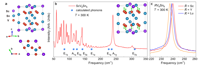
Figure 1b summarizes the Raman scattering response of ScV6Sn6 at room temperature. We employ a symmetry analysis, complementary lattice dynamics calculations, polarizer/analyzer combinations, and chemical substitution on the site to assign the excitations. Overall, the eight calculated phonon frequencies (blue spheres in Fig. 1b, see Supplementary Table II) are in excellent agreement with the measured spectrum. Challenging assignments are near 240 cm-1 where there are two candidate modes and below 200 cm-1 where the Raman-active phonons are embedded in a series of extra peaks. The latter turn out to be rotational modes of air in the optical path. They appear in this and other measurements of ScV6Sn6 39; 38 due to the low brightness of the sample. The peak near 240 cm-1 is important in our continuing discussion. According to our lattice dynamics calculations, there are two candidates for this structure: and symmetry modes. Surprisingly, the peak can be fit by a single oscillator suggesting that one of these constituents is present with extremely low intensity. Based upon extinction behavior under various polarizer/analyzer arrangements [Supplementary figure 1 c], we assign the 240 cm-1 peak as primarily an symmetry mode. The displacement pattern, which involves out-of-plane V center motion, is shown in the inset of Fig. 1b. Substitution on the (Sc) site is less useful for assignment purposes because the frequency vs. mass trend is not straightforward [Fig. 1c]. The atomic radius of the center and the precise local environment appear to be more important. The complete set of mode assignments in ScV6Sn6 is given in Supplementary Table 1.
Symmetry breaking across the CDW transition
Figure 2a summarizes the Raman scattering response of ScV6Sn6 as a function of temperature in the high frequency region. We focus on the behavior of the symmetry mode near 240 cm-1. This structure hardens systematically with decreasing temperature and splits into a cluster of at least five closely-spaced peaks below 90 K. 111The low brightness of this sample and resolution issues make it difficult to tell whether the small shoulders and tiny features on the baseline are real - sufficiently different from nearby peaks as well as the noise level. This cluster is the most conspicuous signature of the CDW phase, although it obviously raises questions of exactly how and why a singly-degenerate vibrational mode might split in a low symmetry environment. We show the behavior of the phonon near 300 cm-1 for comparison. This structure hardens anharmonically with decreasing temperature but does not split across - in line with the other Raman-active modes in ScV6Sn6 including those of symmetry. Complementary measurements of LuV6Sn6 and YV6Sn6 reveal no low temperature splitting of the 240 cm-1 mode [Supplemental figure 2], consistent with transport results indicating the absence of CDW transitions in the = Lu and Y analogs.23; 21 This again demonstrates that multiplet splitting of the symmetry mode is a signature of the unusual CDW state in ScV6Sn6.
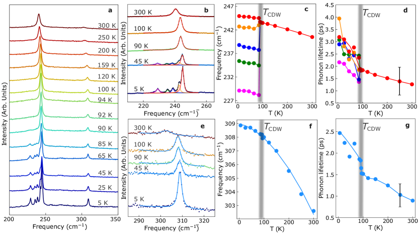
We quantify these results by fitting the Raman scattering response of ScV6Sn6 with a series of Voigt oscillators and a linear baseline. Close-up views of the modes of interest along with their oscillator fits are shown in Fig. 2b,e. A single oscillator is required to fit the symmetry mode in the normal state whereas a minimum of five oscillators are needed to fit the spectra in the CDW state. By contrast, a single oscillator fits the mode near 300 cm-1 over the full temperature range. The center frequency and full width at half maximum (FWHM) are extracted from these fits. The phonon lifetime is a useful quantity related to the Heisenberg uncertainty principle that can be calculated as .41
Figure 2c,d displays frequency and phonon lifetime trends as a function of temperature for the symmetry phonon. The sharp peak splitting immediately below is consistent with a first-order phase transition,30; 25; 31; 32 although as we shall see below, the splitting is not due to symmetry breaking induced splitting of components of a single mode because a singly-degenerate vibrational mode cannot not split further as part of a group-subgroup transition. At the same time, the strong clustering seems to argue against the appearance of traditional zone-folded phonons unless the phonon bands are rather flat and fold into a similar frequency window. 37; 42; 43 Overall, the phonon lifetime rises from 1.25 ps at room temperature to between 2.2 and 4 ps in the low temperature phase depending on the branch.
Figure 2f,g displays frequency and phonon lifetime of the phonon as a function of temperature. The mode hardening can be modeled by characteristic anharmonic effects 44 where with , . Here, is the characteristic frequency at base temperature, and are constants. There are no anomalies in the frequency vs. temperature curve near the CDW transition. On the other hand, the phonon lifetime shows a pronounced kink at , rising sharply toward a limiting low temperature value of 2.5 ps. We carried out a similar analysis of the lower frequency phonons in ScV6Sn6 as well. No additional peak splitting or unusual phonon softening was identified within our sensitivity, although we emphasize that ScV6Sn6 is a very low brightness sample. Thus, the dramatic peak splitting of the 240 cm-1 symmetry vibrational mode is key to understanding the CDW transition.
| + + | ||
| + + |
Phonon mixing in the low temperature phase
In order to better understand the multiplet structure of the 240 cm-1 phonon, we performed a symmetry analysis of the phonon modes. 45 In particular, we solved the subduction problem which relates the irreps of the high-temperature structure and the low-temperature structure [Table 1]. This is a powerful technique that unravels a set of perturbed modes in terms of unperturbed vibrational modes.46; 47 As expected, irreps in , which exhibit the full crystal symmetry of the structure, also exhibit the full crystal symmetry of the subgroup , and thus map to in as well. This irrep is Raman-active in both structures, but is only one-dimensional - the single peak at 240 cm-1 in the high-temperature structure cannot, on its own, account for all five new modes in the structure. Where, then, do the new modes come from?
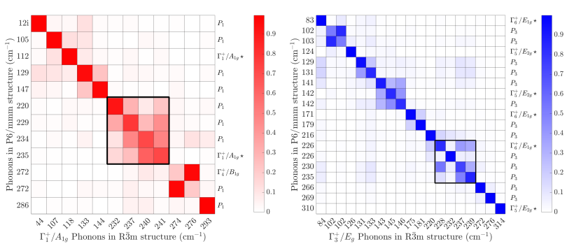
The results in Table 1 show that new Raman active modes can appear in from the modes of at the zone center, as well as and modes which fold in to from the point on the Brillouin zone boundary in reciprocal space (defined in Supplementary table S3). In order to gain a quantitative understanding of the origin of each mode, we perform an analysis where the eigenvectors of the dynamical matrix associated with each phonon mode in the structure are projected onto the eigenvectors of the dynamical matrix in the structure as described in the Methods section. While all symmetry-allowed phonon modes are allowed to mix in the formation of the phonon modes (for example, a given mode could exhibit significant contributions from multiple , , and modes simultaneously), this technique allows us to understand the relative magnitudes of those contributions. The results shown in Fig. 3 show eight Raman-active phonon modes in the range of 228 cm-1 to 241 cm-1 in the structure, which exhibit significant overlap with , , , and phonon modes in the range of 220 cm-1 to 235 cm-1 in the structure. Thus, the five clear peaks that result from the apparent splitting of the peak at 240 cm-1 observed in experiment are likely a subset of these eight modes, and therefore originate not just from the peak at 240 cm-1, but from modes as well as modes at the point in reciprocal space which fold in to the point and become Raman-active in the structure.
Pressure destabilizes the CDW transition
Figure 4 summarizes the Raman scattering response of ScV6Sn6 under pressure at room temperature. We focus on the behavior of the symmetry phonon near 240 cm-1 because (i) it is most strongly connected to the CDW state and (ii) all other modes show only simple hardening under compression - at least within our sensitivity. As indicated in Fig. 4a,b, this peak can be modeled with a single oscillator below 2 GPa and also above approximately 6 GPa. At intermediate pressures, the spectra of ScV6Sn6 are best fit with two Voigt oscillators indicating the presence of a mixed phase. This type of mixed or two-phase regime is typical for a first-order pressure-driven transition. 48 In this case, the mixed phase consists of + a new high pressure phase. Based on this behavior, we define two critical pressures: = 2 GPa and = 6 GPa.
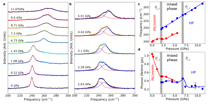
Figure 4c,d displays frequency vs. pressure and phonon lifetime trends for ScV6Sn6. We find that the concentration of (as measured by the relative strength of the low frequency oscillator) diminishes with increasing compression in the mixed phase region whereas that of the new high pressure phase (measured by the relative strength of the second peak) increases until it dominates above . The high pressure phase of ScV6Sn6 is very similar to but not identical to . The single -like phonon mode emerging above has a higher frequency than that in the ground state, pointing to a stronger force constant as well as a volume reduction in the high pressure phase which may have interesting connections to the inter-layer coupling in this class of kagomé metals. At the same time, phonon lifetime drops from 1 ps at ambient pressure (lower than most traditional semiconductors and chalcogenides) to approximately 0.2 ps over this range. The decreased lifetime is due to significantly increased scattering events under compression. 41 We mention in passing that we could not stabilize the high pressure phase in our first principles simulations under pressure. This may be due to complications from the residual density wave state recently reported at room temperature or some other shortcoming of density functional theory.31; 32
Prior transport studies reveal that the structure of ScV6Sn6 starts to change near 2 GPa due to destabilization and disappearance of the CDW. 24 It is tempting to claim that this destabilization corresponds to , but we must remember that our measurements are performed at room temperature - where the CDW is not fully developed. The recently reported short range CDW provides a way forward. This “residual CDW” resides in the high temperature phase of ScV6Sn6 and hosts a (1/3,1/3,1/2) propagation vector. 31; 32 We hypothesize that pressure quenches short range CDW correlations in this system as well, although it appears to do so in a first-order mixed phase manner between and .
There are not too many parallels between the pressure induced transition we observe here in ScV6Sn6 and those observed in the single-layer vanadate kagomés like V3Sb5, because the latter takes place at low temperature and between two different long-range-ordered CDW phases and the high symmetry phase, whereas in ScV6Sn6 this transition takes place at room temperature, well above the long-range CDW order.49; 50; 51 A possibility that explains the disappearance of CDW at high pressures is that the system undergoes a volume-collapse transition similar to those observed in the ThCr2Si2 family of compounds, which involves the formation of Sn–Sn covalent bonds.52; 53 Such transitions are also observed in various iron-pnictide superconductors, and couple strongly to superconductivity because of their effect on the Fermi surface54; 55. Therefore, such a transition is likely to suppress CDW as well.
Finally, we note that similar measurements on the Lu analog reveal no evidence at all for this type of pressure-induced destabilization of the short range CDW [Supplementary figure 3]. The A1g symmetry mode near 240 cm-1 hardens systematically under compression in line with the fact that LuV6Sn6 does not host a CDW. 56 These structure-property relations are nicely unified by site size arguments [Inset, supplementary figure 1d] which reveal that both chemical and physical pressure drive similar trends in CDW stability.
Unraveling CDW stability in the V6Sn6 family of materials ( = Sc, Y, Lu)
Traditionally, CDW behavior is related to a periodic lattice modulation due to Fermi surface nesting and electron-phonon interactions.57; 58; 59; 60; 61; 62 Unraveling the complete mechanism requires a systematic investigation of the electronic structure as well as a full exploration of the vibrational properties. In this family of materials, most of the focus so far has been on electronic properties from the point of view of electron-phonon coupling and Fermi surface nesting.63; 64; 65; 38; 66 There has been significantly less effort to uncover the vibrational contribution to the development of the density wave state. This is because metallic character in both high and low temperature phases of ScV6Sn6 prevents us from revealing the behavior of the infrared-active phonons due to screening by the Drude peak. The Raman scattering response is, however, still accessible, and combined with different external stimuli and complementary lattice dynamics calculations, a remarkable picture of phonon mixing and density wave stability is beginning to emerge.
In this work, we traced how phonons mix in the CDW state of ScV6Sn6, tested these ideas with symmetry arguments based upon our lattice dynamics calculations, and compared our findings to behavior in the Y and Lu analogs. Overall, we demonstrate that low temperature stabilizes the CDW whereas both physical and chemical pressures destroy it. This suggests that the coupling interactions are on the “knife’s edge”, easily manipulated by any external stimuli, and more sensitive than the similar CDW orders in the monolayer AV3Sb5 vanadates. Our analysis reveals that the multiplet-like behavior of the 240 cm-1 phonon in the CDW state of ScV6Sn6 is the result of its mixing with other phonons. We emphasize that this splitting is not due to symmetry breaking of a single mode in the conventional sense. Instead, it is connected with both and point modes that are folded to the zone center and become Raman active, indicating that the CDW state is influenced by a variety of phonon modes and highlighting the intricate, phonon-assisted nature of the CDW state. Since the phonon mode near 240 cm-1 also serves to connect the short-range and long-range CDWs, it provides a sensitive, microscopic indicator of CDW stability under different tuning parameters. Finally, we point out that while prior phonon dispersion calculations emphasize the role of unstable Sn and Sc modes in the CDW state, 33 this and other work 25; 64; 66 is revealing that the V centers are not just spectators. Rather, the out-of-plane motion of V in the double kagomé layer is just as significant as the Sc and Sn center motion. Recent STM work reaches a similar conclusion regarding the importance of the V centers. 64
Methods
Crystal growth and diamond anvil cell loading:
High quality V6Sn6 (= Sc, Lu, Y) crystals were grown from a Sn-rich melt method with a composition ratio of :V:Sn = 1:6:60 as described in Ref. 25. They are hexagonal blocks with clear surfaces. For the high pressure Raman scattering measurements, a small single crystal was loaded into a symmetric diamond anvil cell suitable for work in the 0 - 13 GPa range. The cell is equipped with low fluorescence diamonds with 400 m culets. We also employed a stainless steel gasket with a 100 m hole, KBr as the pressure medium, and an annealed ruby ball for pressure determination via fluorescence. 67
Raman spectroscopy:
Raman scattering measurements were performed in the back scattering geometry using a Horiba LabRAM HR Evolution spectrometer equipped with a 532 nm (green) laser, a 50 microscope objective, 1800 line/mm gratings, and a liquid-nitrogen-cooled charge-coupled device detector. To minimize heating and maximize signal intensity for this low brightness sample, power was controlled below 7.7 mW, and the laser was slightly defocused. Each spectrum was integrated for 200 s and averaged four times. Variable temperature work was carried out with a low-profile open-flow cryostat, and high pressure measurements employed a diamond anvil cell as described above. Standard peak fitting techniques were employed as appropriate.
Lattice dynamics calculations:
All density functional theory (DFT) calculations were performed with Projector Augmented Waves (PAW) as implemented in the Vienna Ab initio simulation package (VASP) version 5.4.4 68; 69; 70 using the PBEsol exchange-correlation functional for valence configurations of Sc, V, and Sn corresponding to 3s23p64s13d2, 3s23p64s13d4, and 5s24d105p2, respectively. Unless otherwise mentioned, experimentally determined lattice parameters of Å and Å for the structure and Å and Å for the conventional structure were used for all calculations Internal degrees of freedom were relaxed, with forces converged to within 0.001 eV/Å using a plane wave cutoff energy of 400 eV, combined with a -centered Monkhorst-Pack k-point mesh of 202010 in the structure, as well as a Gaussian smearing parameter of 10 meV. Calculations in the structure were carried out in a primitive, three formula-unit cell commensurate with the wavevector , which corresponds to a unit cell with basis vectors , where the indices correspond to the lattice vectors of the conventional nine formula unit cell. All computational parameters used for this structure were the same as for the structure, except with a -centered Monkhorst-Pack k-point mesh of 101010. To calculate phonon frequencies and their associated distortions, we constructed the dynamical matrix in a basis of symmetry adapted modes, which bring the dynamical matrix into block diagonal form, where each block corresponds to a single irreducible representation of the space group. These symmetry-adapted linear combinations of atomic displacements were found using the ISOTROPY software suite. 71
Phonon overlap:
After calculating the eigenvectors of the dynamical matrix associated with each phonon mode, we then computed the relationship between eigenvectors in the structure (where is an irrep, the mode index within that irrep, and the ionic degree of freedom in cartesian coordinates), and the eigenvectors in the structure. First, the were expressed in a three formula unit basis commensurate with the cell, then renormalized. The overlap for two phonons is then defined as the projection of onto ,
| (1) |
In the lefthand panel of Fig. 3, , and , as determined by the solution to the subduction proble described in Table 1. In the righthand panel, , and . In this second case, the and phonons are doubly degenerate, and the phonons quadruply degenerate. In order to compress the results of the table, instead of reporting a cell for each individual degenerate mode, our figure includes a single cell with amplitude defined as , where
Group Theory:
The symmetry-adapted linear combinations of atomic displacements used for the phonon calculations were found using the ISOTROPY software suite.71 The subduction analysis to find the connections between irreps through the group-subgroup transition was performed using the CORREL application hosted by the Bilbao crystallographic server.45
Data availability
Data are available from the corresponding authors upon reasonable request.
Acknowledgements
Work at Tennessee (YG, KAS, ALB, and JLM) is supported by Physical Behavior of Materials, Basic Energy Sciences, U.S. Department of Energy (Contract number DE-SC00023144). DM and WRM acknowledges funding from the Gordon and Betty Moore Foundation’s EPiQS Initiative, Grant GBMF9069. Work at the University of Minnesota (ETR and TB) was supported by NSF CAREER grant DMR-2046020.
Author contributions
YG and JLM designed the study. WRM, SM, and RPM grew the crystals with guidance from DGM. ALB carried out feasibility measurements while YG performed the variable temperature and high pressure Raman scattering spectroscopy. ER performed the theoretical calculations and discussed the results with TB. YG and KAS analysed the spectral data with guidance from JLM. YG, ER, and JLM wrote the manuscript. All authors commented on the text.
Competing interests
The authors declare no competing financial or non-financial interests.
References
- (1) Kang, M. et al. Dirac fermions and flat bands in the ideal kagome metal FeSn. Nature materials 19, 163–169 (2020).
- (2) Li, M. et al. Dirac cone, flat band and saddle point in kagome magnet YMn6Sn6. Nature communications 12, 3129 (2021).
- (3) Liu, Z. et al. Orbital-selective Dirac fermions and extremely flat bands in frustrated kagome-lattice metal CoSn. Nature communications 11, 4002 (2020).
- (4) Yin, J.-X. et al. Negative flat band magnetism in a spin–orbit-coupled correlated kagome magnet. Nature Physics 15, 443–448 (2019).
- (5) Balents, L. Spin liquids in frustrated magnets. Nature 464, 199–208 (2010).
- (6) Yan, S., Huse, D. A. & White, S. R. Spin-liquid ground state of the S= 1/2 kagome Heisenberg antiferromagnet. Science 332, 1173–1176 (2011).
- (7) Meier, W. R. et al. Flat bands in the CoSn-type compounds. Phys. Rev. B 102, 075148 (2020).
- (8) Paul, A., Chung, C.-M., Birol, T. & Changlani, H. J. Spin-lattice Coupling and the Emergence of the Trimerized Phase in the S= 1 Kagome Antiferromagnet Na2Ti3Cl8. Phys. Rev. Lett. 124, 167203 (2020).
- (9) Ye, L. et al. Massive Dirac fermions in a ferromagnetic kagome metal. Nature 555, 638–642 (2018).
- (10) Lachman, E. et al. Exchange biased anomalous Hall effect driven by frustration in a magnetic kagome lattice. Nature communications 11, 560 (2020).
- (11) Tanaka, M. et al. Topological Kagome magnet Co3Sn2S2 thin flakes with high electron mobility and large anomalous Hall effect. Nano Lett. 20, 7476–7481 (2020).
- (12) Xu, G., Lian, B. & Zhang, S.-C. Intrinsic quantum anomalous hall effect in the kagome lattice Cs2LiMn3F12. Phys. Rev. Lett. 115, 186802 (2015).
- (13) Rüegg, A. & Fiete, G. A. Fractionally charged topological point defects on the kagome lattice. Phys. Rev. B 83, 165118 (2011).
- (14) Feng, Z. et al. Gapped spin-1/2 spinon excitations in a new kagome quantum spin liquid compound Cu3Zn(OH)6FBr. Chinese Physics Letters 34, 077502 (2017).
- (15) Ghimire, N. J. et al. Competing magnetic phases and fluctuation-driven scalar spin chirality in the kagome metal YMn6Sn6. Science Advances 6, eabe2680 (2020).
- (16) Wang, Q. et al. Field-induced topological Hall effect and double-fan spin structure with a -axis component in the metallic kagome antiferromagnetic compound . Phys. Rev. B 103, 014416 (2021).
- (17) Teng, X. et al. Magnetism and charge density wave order in kagome FeGe. Nature Physics 1–9 (2023).
- (18) Ortiz, B. R. et al. New kagome prototype materials: discovery of KV3Sb5, RbV3Sb5, and CsV3Sb5. Phys. Rev. Mater. 3, 094407 (2019).
- (19) Ortiz, B. R. et al. CsV3Sb5: A topological kagome metal with a superconducting ground state. Phys. Rev. Lett. 125, 247002 (2020).
- (20) Teng, X. et al. Discovery of charge density wave in a kagome lattice antiferromagnet. Nature 609, 490–495 (2022).
- (21) Pokharel, G. et al. Electronic properties of the topological kagome metals and . Phys. Rev. B 104, 235139 (2021).
- (22) Hu, Y. et al. Tunable topological Dirac surface states and van Hove singularities in kagome metal GdV6Sn6. Science Advances 8, eadd2024 (2022).
- (23) Zhang, X. et al. Electronic and magnetic properties of intermetallic kagome magnets . Phys. Rev. Mater. 6, 105001 (2022).
- (24) Zhang, X. et al. Destabilization of the charge density wave and the absence of superconductivity in ScV6Sn6 under high pressures up to 11 GPa. Materials 15, 7372 (2022).
- (25) Arachchige, H. W. S. et al. Charge density wave in kagome lattice intermetallic ScV6Sn6. Phys. Rev. Lett. 129, 216402 (2022).
- (26) Ritz, E. T. et al. Orbital-selective electron-phonon coupling and superconductivity in av3sb5. arXiv preprint arXiv:2304.14822 (2023).
- (27) Zhao, H. et al. Cascade of correlated electron states in the kagome superconductor CsV3Sb5. Nature 599, 216–221 (2021).
- (28) Liang, Z. et al. Three-dimensional charge density wave and surface-dependent vortex-core states in a kagome superconductor . Phys. Rev. X 11, 031026 (2021).
- (29) Du, F. et al. Pressure-induced double superconducting domes and charge instability in the kagome metal . Phys. Rev. B 103, L220504 (2021).
- (30) Hu, T. et al. Optical spectroscopy and band structure calculations of the structural phase transition in the vanadium-based kagome metal . Phys. Rev. B 107, 165119 (2023).
- (31) Cao, S. et al. Competing charge-density wave instabilities in the kagome metal ScV6Sn6. arXiv preprint arXiv:2304.08197 (2023).
- (32) Korshunov, A. et al. Softening of a flat phonon mode in the kagome ScV6Sn6. arXiv preprint arXiv:2304.09173 (2023).
- (33) Tan, H. & Yan, B. Abundant lattice instability in kagome metal ScV6Sn6. arXiv preprint arXiv:2302.07922 (2023).
- (34) Fan, S. et al. Electronic chirality in the metallic ferromagnet . Phys. Rev. B 96, 205119 (2017).
- (35) Fan, S. et al. Excitations of intercalated metal monolayers in transition metal dichalcogenides. Nano Lett. 21, 99–106 (2020).
- (36) Wu, S. et al. Charge density wave order in the kagome metal . Phys. Rev. B 105, 155106 (2022).
- (37) Liu, G. et al. Observation of anomalous amplitude modes in the kagome metal CsV3Sb5. Nature communications 13, 3461 (2022).
- (38) Hu, Y. et al. Phonon promoted charge density wave in topological kagome metal ScV6Sn6 . arXiv preprint arXiv:2304.06431 (2023).
- (39) Ohno, H., Iizuka, Y. & Fujita, S. Pure rotational raman spectroscopy applied to N2/O2 analysis of air bubbles in polar firn. Journal of Glaciology 67, 903–908 (2021).
- (40) The low brightness of this sample and resolution issues make it difficult to tell whether the small shoulders and tiny features on the baseline are real - sufficiently different from nearby peaks as well as the noise level.
- (41) Sun, Q.-C. et al. Spectroscopic determination of phonon lifetimes in rhenium-doped MoS2 nanoparticles. Nano Lett. 13, 2803–2808 (2013).
- (42) Joshi, J. et al. Short-range charge density wave order in . Phys. Rev. B 99, 245144 (2019).
- (43) Hill, H. M. et al. Phonon origin and lattice evolution in charge density wave states. Phys. Rev. B 99, 174110 (2019).
- (44) Balkanski, M., Wallis, R. F. & Haro, E. Anharmonic effects in light scattering due to optical phonons in silicon. Phys. Rev. B 28, 1928–1934 (1983).
- (45) Aroyo, M. I., Kirov, A., Capillas, C., Perez-Mato, J. & Wondratschek, H. Bilbao Crystallographic Server. II. Representations of crystallographic point groups and space groups. Acta Crystallographica Section A: Foundations of Crystallography 62, 115–128 (2006).
- (46) Long, V. C. et al. Far-infrared vibrational properties of high-pressure high-temperature polymers and the dimer. Phys. Rev. B 61, 13191–13201 (2000).
- (47) Zhu, Z.-T. et al. Far-infrared vibrational properties of tetragonal polymer. Phys. Rev. B 65, 085413 (2002).
- (48) Musfeldt, J., Mandrus, D. & Liu, Z. Insulator–metal transition in CrSiTe3 triggered by structural distortion under pressure. npj 2D Materials and Applications 7, 28 (2023).
- (49) Zhang, Z. et al. Pressure-induced reemergence of superconductivity in the topological kagome metal csv3sb5. Phys. Rev. B 103, 224513 (2021).
- (50) Gupta, R. et al. Two types of charge order with distinct interplay with superconductivity in the kagome material CsV3Sb5. Communications Physics 5, 232 (2022).
- (51) Ritz, E. T., Fernandes, R. M. & Birol, T. Impact of Sb degrees of freedom on the charge density wave phase diagram of the kagome metal CsV3Sb5. arXiv preprint arXiv:2212.13319 (2022).
- (52) Hoffmann, R. & Zheng, C. Making and breaking bonds in the solid state: The ThCr2Si2 structure. The Journal of Physical Chemistry 89, 4175–4181 (2002).
- (53) Foroozani, N. et al. Hydrostatic high-pressure studies to 25 GPa on the model superconducting pnictide LaRu2P2. In Journal of Physics: Conference Series, vol. 500, 032007 (IOP Publishing, 2014).
- (54) Kreyssig, A. et al. Pressure-induced volume-collapsed tetragonal phase of as seen via neutron scattering. Phys. Rev. B 78, 184517 (2008). URL https://link.aps.org/doi/10.1103/PhysRevB.78.184517.
- (55) Saha, S. et al. Structural collapse and superconductivity in rare-earth-doped CaFe2As2. Phys. Rev. B 85, 024525 (2012).
- (56) Lee, J. & Mun, E. Anisotropic magnetic property of single crystals V6Sn6 ( = Y, Gd-Tm, Lu). Phys. Rev. Mater. 6, 083401 (2022).
- (57) Zhu, X., Cao, Y., Zhang, J., Plummer, E. & Guo, J. Classification of charge density waves based on their nature. Proceedings of the National Academy of Sciences 112, 2367–2371 (2015).
- (58) Grüner, G. & Zettl, A. Charge density wave conduction: A novel collective transport phenomenon in solids. Physics Reports 119, 117–232 (1985).
- (59) Roy, A. P., Bajaj, N., Mittal, R., Babu, P. D. & Bansal, D. Quasi-One-Dimensional Fermi Surface Nesting and Hidden Nesting Enable Multiple Kohn Anomalies in -Uranium. Phys. Rev. Lett. 126, 096401 (2021).
- (60) Brouet, V. et al. Fermi Surface Reconstruction in the CDW State of CeTe3 Observed by Photoemission. Phys. Rev. Lett. 93, 126405 (2004).
- (61) Weber, F. et al. Electron-phonon coupling and the soft phonon mode in TiSe2. Phys. Rev. Lett. 107, 266401 (2011).
- (62) Jurczek, E. & Rice, T. A charge-density-wave instability in BaBi1-xPbxO3 caused by strong electron-phonon coupling. Europhysics Letters 1, 225 (1986).
- (63) Lee, S. et al. Nature of charge density wave in kagome metal ScV6Sn6 (2023). eprint 2304.11820.
- (64) Cheng, S. et al. Nanoscale visualization and spectral fingerprints of the charge order in ScV6Sn6 distinct from other kagome metals. arXiv preprint arXiv:2302.12227 (2023).
- (65) Kang, S.-H. et al. Emergence of a new band and the Lifshitz transition in kagome metal ScV6 Sn6 with charge density wave. arXiv preprint arXiv:2302.14041 (2023).
- (66) Tuniz, M. et al. Dynamics and resilience of the charge density wave in a bilayer kagome metal. arXiv preprint arXiv:2302.10699 (2023).
- (67) Mao, H., Bell, P., Shaner, J. t. & Steinberg, D. Specific volume measurements of Cu, Mo, Pd, and Ag and calibration of the ruby R1 fluorescence pressure gauge from 0.06 to 1 Mbar. Journal of applied physics 49, 3276–3283 (1978).
- (68) Kresse, G. & Hafner, J. Ab initio molecular dynamics for liquid metals. Phys. Rev. B 47, 558 (1993).
- (69) Kresse, G. & Furthmüller, J. Efficiency of ab-initio total energy calculations for metals and semiconductors using a plane-wave basis set. Comput. Mater. Sci. 6, 15–50 (1996).
- (70) Kresse, G. & Furthmüller, J. Efficient iterative schemes for ab initio total-energy calculations using a plane-wave basis set. Phys. Rev. B 54, 11169 (1996).
- (71) Stokes, H., Hatch, D. & Campbell, B. ISOTROPY Software Suite v. 9.6.1. iso.byu.edu (2022).
- (72) Johannes, M. D. & Mazin, I. I. Fermi surface nesting and the origin of charge density waves in metals. Phys. Rev. B 77, 165135 (2008).
- (73) Hoesch, M., Bosak, A., Chernyshov, D., Berger, H. & Krisch, M. Giant Kohn Anomaly and the Phase Transition in Charge Density Wave . Phys. Rev. Lett. 102, 086402 (2009).
- (74) Varma, C. M. & Simons, A. L. Strong-Coupling Theory of Charge-Density-Wave Transitions. Phys. Rev. Lett. 51, 138–141 (1983).