2021
1]\orgdivCentre de Nanosciences et de Nanotechnologies (C2N), \orgnameUMR CNRS 9001, \orgnameUniversité Paris-Saclay, \orgaddress\street10 Boulevard Thomas Gobert, \cityPalaiseau, \postcode91120, \countryFrance
2]\orgdivLaboratoire de Physique et d’Étude des Matériaux, \orgnameUMR CNRS 8213, \orgnameESPCI Paris, \orgnameUniversité PSL, \orgnameSorbonne Université, \orgaddress\street10 Rue Vauquelin, \cityParis, \postcode75005, \countryFrance
3]\orgdivAdvanced Mesoscience and Nanotechnology Centre, \orgnameMoscow Institute of Physics and Technology, \orgaddress\cityDolgoprudny, \postcode141700, \countryRussia
4]\orgdivAdvanced Mesoscience and Nanotechnology Centre, \orgnameNational University of Science and Technology MISIS, \orgaddress\cityMoscow, \postcode119049, \countryRussia
5]\orgdivM.N. Mikheev Institute of Metal Physics, \orgnameUB RAS, \orgaddress\cityEkaterinburg, \postcode620108, \countryRussia
6]\orgdivInstitut des NanoSciences de Paris, \orgnameUMR CNRS 7588, \orgnameSorbonne Université, \orgaddress\street4 Place Jussieu, \cityParis, \postcode75005, \countryFrance
7]\orgdivInstitute of Ion Beam Physics and Materials Research, \orgnameHelmholtz-Zentrum Dresden-Rossendorf, \cityDresden, \postcode01328, \countryGermany
8]\orgdivDepartment of Applied Physics, \orgnameAalto University, P.O. Box 11100, \cityAalto, \postcode00076, \countryFinland
Hydrogenic Spin-Valley states of the Bromine donor in 2H-MoTe2
Abstract
In semiconductors, the identification of doping atomic elements allowing to encode a qubit within spin states is of intense interest for quantum technologies. In transition metal dichalcogenides semiconductors, the strong spin-orbit coupling produces locked spin-valley states with expected long coherence time. Here we study the substitutional Bromine BrTe dopant in 2H-MoTe2. Electron spin resonance measurements show that this dopant carries a spin with long-lived nanoseconds coherence time. Using scanning tunneling spectroscopy, we find that the hydrogenic wavefunctions associated with the dopant levels have characteristics spatial modulations that result from their hybridization to the Q-valleys of the conduction band. From a Fourier analysis of the conductance maps, we find that the amplitude and phase of the Fourier components change with energy according to the different irreducible representations of the impurity-site point-group symmetry. These results demonstrate that a dopant can inherit the locked spin-valley properties of the semiconductor and so exhibit long spin-coherence time.
1 Introduction
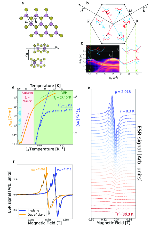
In zinc-blende III-V semiconductors, the large spin-orbit coupling leads to spin mixing and loss of spin coherence. This motivated the use of silicon, characterized by weak spin-orbit coupling, as a host of dopants for qubits Zwanenburg2013-ak ; Salfi2014-ns ; Usman2016-dh ; Voisin2020-ar . In contrast, in 2H-transition metal dichalcogenides (TMDCs), the combination of strong spin-orbit coupling and multiple valleys in the band structure provides protection against relaxation and decoherence. Indeed, due to the horizontal mirror symmetry of the crystal structure, shown in Fig. 1a, the spin projection remains a good quantum number in the whole Brillouin zone, shown in Fig. 1b, even in the presence of strong spin-orbit coupling that lifts the degeneracy of the bands of opposite spin polarization. Furthermore, the electronic states are characterized by an additional index, the valley index, which is locked to the spin index Zhu2011-ss ; Xiao2012-sz ; Kosmider2013-jb ; Liu2013-rm ; Roldan2014-dz ; Liu2015-ju ; Kormanyos2015-bt . This reduces the sensitivity of the spin to scattering processes because spin and valley indexes must change simultaneously. For this reason, numerous theoretical works have considered the spin-valley states hosted within 2H-TMDCs for encoding qubits Rohling2012-mx ; Kormanyos2014-vt ; Wu2016-ku ; Pearce2017-xz ; Szechenyi2018-jf ; David2018-he ; Pawlowski2018-xh . Furthermore, it has been shown that Moiré lattices of spin-valley states could be used to simulate correlated Wu2018-ly ; Schrade2019-mn and topological Wu2019-qf systems with recent experimental results obtained on twisted TMDCs bilayersWang2020-pq ; Tang2020-lo ; Regan2020-ai ; Li2021-yx ; Li2021-qx .
In monolayers, the valley of lowest (highest) energy in the conduction (valence) bands are located at the two nonequivalents K and points of the Brillouin zone. They are related by time reversal symmetry and the two Bloch states and are Kramers partners capable of forming a qubit. To zeroth-order, spin-flip implies a change of valley and so the quantum states are protected from scattering by acoustic long-wavelength phonons Song2013-uo ; Gilardoni2021-sv . Time-resolved Kerr rotation measurements of the spin polarization of resident carriers have demonstrated spin lifetime reaching 100 ns for band electrons Yang2015-ww ; Ersfeld2019-ol , 4 to 40 ns for localized electrons Yang2015-hq ; Jiang2022-ua and 1 s for holes Dey2017-tm .
As the manipulation of one qubit requires the spin state to be localized spatially, this motivates the identification of dopants that inherit the locked spin-valley properties of the TMDC semiconductors. For this to happen, the dopant atomic orbitals must hybridize with the valley Bloch states and these Bloch states of opposite spin and valley polarization should not be mixed by the dopant confining potential. This means that each dopant quantum state should be formed from either the -valley or -valley but not both. As detailed in Supplementary, group theory Evarestov1986-ct shows that, for a dopant located on the anion site, the hybridization of the p-orbitals and the Bloch states at the K- and Q-valley is allowed by symmetry. Furthermore, it was shown Liu2014-vy ; Wu2016-ku ; Kaasbjerg2017-ta that inter-valley mixing is forbidden by the C3 symmetry of the anion site.
These conditions prompt the use of elements from column V (VII) as p (n) type dopants substituting the anion site. The formation of donor states near the conduction band by halogen dopants substituting the anion site has been confirmed by first principles calculations Komsa2012-md ; Dolui2013-wx ; Guo2017-xy ; Onofrio2017-lz , with BrTe having one of the lowest formation energies Onofrio2017-lz . Furthermore, BrTe has been identified as an n-type dopant in earlier transport measurements Morsli1997-tu and MoTe2 has the largest spin-orbit coupling in the conduction band among Mo-based TMDCs.
In this work, we identify the BrTe spin signal by electron spin resonance (ESR) and relates the spin lifetime to the electronic properties obtained from transport measurements and angular resolved photoemission spectroscopy (ARPES). By scanning tunneling microscopy and spectroscopy (STM/STS), we demonstrate that the dopant levels are hydrogenic states hybridized to the Q-valleys of the conduction band.
2 Results
The MoTe2 crystal samples were grown by chemical vapor transport using Bromine gas as transport agent and doping source. To enable the preparation of Ultra-High Vacuum (UHV) clean surfaces by cleavage and because of insufficient sensitivity of standard ESR at measuring atomic monolayers of materials, we worked with bulk crystals. As discussed in Ref. Zhang2014-ng , while the global inversion symmetry is restored in bulk materials, the local inversion symmetry is still broken, meaning that the bulk material can be described as a stack of distinguishable layers. This picture has been confirmed by the observation of hidden spin-polarization of valleys Riley2014-hd ; Razzoli2017-dv ; Tu2020-zd by spin-resolved ARPES and by measurements of valley orbital magnetic moment and Berry phase using circular-dichroism ARPES Cho2018-hu ; Beaulieu2020-np .
2.1 ARPES and transport measurements
Fig. 1c shows an ARPES spectra in -K direction measured on Br-doped MoTe2. The band contours and the spin-orbit splitting of the valence band, meV, are consistent with DFT calculations Liu2013-rm . At the -point, the valence band is about 1 eV below the Fermi energy, which implies that the bulk energy band-gap is about 1 eV as expected for MoTe2 Liu2013-rm ; Han2021-tr and that the Fermi energy is in the conduction band. The transport properties are shown in Fig. 1d and Supplementary. From 300 K to 225 K, the resistivity decreases with temperature as expected in the saturation regime, where Hall measurements indicate a carrier concentration about cm-3 and a Hall mobility reaching cm2V-1s-1, see Supplementary. From 100 K to 27 K, the resistivity follows an activated law with activation energy EmeV, consistent with past works on Br-doped MoTe2 Morsli1997-tu . As will be confirmed by STM measurements shown below, this doping level can be described as a rescaled hydrogenic level n=1 with rescaled Bohr radius nm and Rydberg energy meV, where we use for the dielectric constant Grasso1972-hi and the effective mass Kormanyos2015-bt . Below 27 K, the resistivity deviates from the activated law and enters an hopping regime, where the electrons are localized on the dopant and electronic transport occurs through tunnel hopping between the dopants. Below 15 K, the sample resistance is too large to be measurable with standard instruments. Following Ref. Shklovskii1984-vr , the temperature dependence of the resistivity is fitted by a Mott law with the correlation length in two dimensions given by , which provides the temperature scale K. From the correlation length, one obtains the average hopping length . Using the Einstein relation between the mobility and the diffusion constant , the correlation time , i.e., the delay between two hops, is obtained and shown in Fig. 1d. We will show now that this correlation time controls the spin lifetime measured by ESR.
2.2 ESR measurements
Fig. 1e shows the first-derivative ESR signal as a function of the amplitude of an in-plane magnetic field for different temperatures from 30 K down to 8 K. A resonance signal is visible only in the hopping regime, T K, of doped samples. No ESR signal has been observed in undoped samples obtained from HQ graphene. In a recent studyGuguchia2018-gy of undoped 2H-MoTe2, while the signature of magnetism was observed from muon spin rotation measurements, no ESR signal could be observed. Figure 1f shows that the g-factor is anisotropic with = 2.099 ( = 2.018) for the magnetic field perpendicular (parallel) to the sample plane. The anisotropy is opposite, , and smaller than measured on arsenic acceptors in MoS2 Title1973-sh ; Stesmans2016-fq ; Toledo2019-dh . In TMDCs, a larger anisotropy for acceptors than donors is expected given the larger spin-orbit coupling in the valence band. Our value of is consistent with DFT calculations of the spin contribution to the g-factor of localized electronsKormanyos2014-vt ; Pearce2017-xz and Kerr measurements of the g-factor of localized electrons in monolayer MoS2 Yang2015-hq ; Jiang2022-ua . The spectrum is constituted of a central line with additional sidelines and can be described by an effective spin Hamiltonian assuming two different contributions of identical g-tensor. The smallest contribution of weight 0.01 arises from electrons localized on single Br donors, i.e., not experiencing hopping, and produces the sidelines resulting from the hyperfine coupling of the electronic spin with the nuclear spin of the Br nucleus, where both natural isotopes have nuclear spin I = 3/2 for a total abundance of 100. The second, largest, contribution of weight 0.99 produces the central line and arises from the donor electrons hopping between different Br sites, with the hyperfine structure being suppressed due to the different nuclear spin polarizations probed by the electron spin. A similar model was employed for arsenic acceptors in MoS2 Title1973-sh . An analysis of the angular dependence, shown in Supplementary, allows to extract the hyperfine and quadrupolar coupling constants and provides good fitting of the ESR data as shown in Fig. 1f. From the data measured as function of temperature, shown in Supplementary, we obtain the linewidth as function of temperature, from which, the spin coherence Poole1996-zs T is calculated and shown in Fig. 1d, together with the correlation time obtained above. One clearly sees that at the highest temperature, T K, the spin lifetime is controlled by the correlation time, T, with no adjustable parameters. This indicates that strong Elliot-Yafet type dephasing occurs for each hop Meier2012-nr . From this observation, we can conclude that the large spin-orbit coupling in MoTe2 and Elliot-Yafet type dephasing is likely responsible for the disappearance of the resonance signal in the activated regime. Upon cooling into the hopping regime, the correlation time increases rapidly but the spin lifetime seems to saturate at a value T ns, which is similar to the spin lifetime of localized electrons in MoS2 measured by Kerr rotation measurementsYang2015-hq . The origin of this saturation remains to be understood, it could result from scattering with flexural phononsSong2013-uo or exchange coupling between spins. As detailed in supplementary, the hyperfine-limited lifetime should be longer, about 100 ns. As already suggested in numerous previous works Rohling2012-mx ; Song2013-uo ; Kormanyos2014-vt ; Wu2016-ku ; Pearce2017-xz ; Szechenyi2018-jf ; David2018-he ; Pawlowski2018-xh ; Wang2018-sx ; Gilardoni2021-sv , the observation of spin lifetime larger than nanoseconds in TMDCs is likely the consequence of spin-valley locking. We show now STM measurements that indeed demonstrate that the bromine dopant levels are hybridized to the Bloch states of the Q-valleys.
2.3 STM measurements
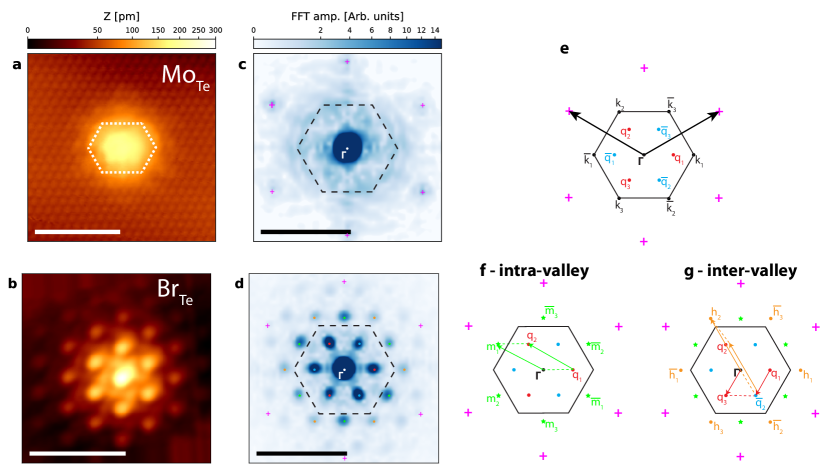
Because the sample becomes insulating at liquid Helium temperature, T= 4.2 K, STM measurements are performed at liquid nitrogen temperature, T= 77 K. Based on previous STM works on undoped MoTe2 Guguchia2018-gy and MoSe2 Edelberg2019-zq as well as DFT calculations Gonzalez2016-rz , we identified the molybdenum antisite MoTe, shown in Fig. 2a, which has a characteristic hexagonal shape. In contrast, we see that the dopant BrTe, Fig. 2b, not observed in undoped samples, has a remarkable spatially modulated structure propagating over an area about 6 nm diameter centered on the original Te atomic site, see Supplementary.
From several large scale topographic images, see Supplementary, the estimated surface density of Br dopants is n cm-2 and corresponds to a bulk carrier density n cm-3, where nm is the length of unit cell along , which is close to the Hall carrier density given above.
Fig. 2cd shows the two-dimensional fast Fourier transforms (2D-FFTs) of the topographic images. For the antisite MoTe, only Bragg peaks are observed. For the dopant, BrTe, instead, the 2D-FFT shows peaks at wavevectors , , resulting from the interference between two Q valleys and peaks at wavevectors , and , , resulting from the interference between Q and valleys.
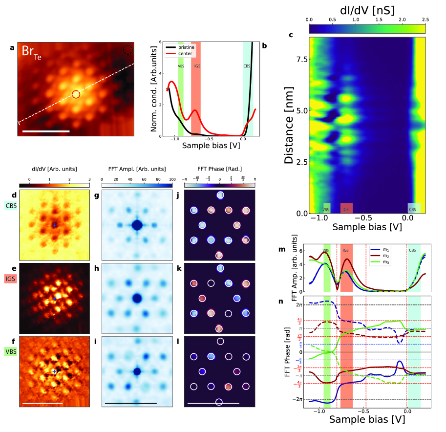
Figure 3b shows the differential conductance , normalized by the integrated differential conductance, as function of sample bias (see methods). A comparison with the spectra measured on the pristine surface allows the identification of three energy ranges where the density of states (DOS) is modified by dopant levels, indicated as conduction band states (CBS) at bias V, in-gap states (IGS) at bias V and valence band states (VBS) at bias V. While a clear peak is only observed for the IGS, the CBS and VBS are merging with the bulk conduction and valence band states, so only shoulders are observed in the differential conductance. However, the CBS and VBS, as well as the IGS, can be clearly identified on Fig. 3c showing the differential conductance as a function of voltage and distance along a profile, indicated as a dashed line on the topographic image, Fig. 3a, running across the dopant. This plot shows that the DOS presents a spatial modulation on these three energy ranges. The conductance maps for the three energy ranges are shown in Fig. 3def. They present distinct spatial patterns but the corresponding 2D-FFTs, Fig. 3ghi, show peaks at the same wavevector coordinates , , identified above. See Supplementary for additional maps at more energies. This modulation is not consistent with QuasiParticle Interferences (QPIs) of conduction electrons scattering on point-defects Roushan2009-zl ; Liu2015-cn . For QPIs, the interferences should be visible around all type of point-defects and the scattering wavevectors coordinates should depend on energy, following the Fermi surface contour. In this case, the Q-valleys interference would be visible only at the top of the conduction band, which is not what is observed experimentally.
Actually, these distinct spatial patterns result from a change of phase relationship between the Fourier components, as visible on the maps of the phase of 2D-FFTs, shown in Fig. 3jkl. Because the phase is not defined for complex numbers of zero amplitude, in these maps, the phase is shown only at k-vectors where the amplitude is large, within white circles. See Supplementary for details. To go further, we extract from the 2D-FFTs the amplitude and the phase of the Fourier components as function of sample bias and plot them Fig. 3m and Fig. 3n, respectively. A peak in the Fourier amplitude is observed within the energy range corresponding to IGS but also for the CBS and VBS, which confirms that dopant-states are formed in these three energy ranges. Within each energy range, the phase remains nearly constant with values equal either a multiple of or a multiple of . In-between, large phase jumps are observed and indicated by vertical red lines in Fig. 3n, at sample bias -0.015, -0.47 and -0.8 V. Similar behavior is observed for the components , shown in Supplementary.
As we will demonstrate now, the spatial modulation of the local DOS results from the hybridization of the dopant orbital levels to the Bloch states at the Q-valley and the phase-jumps are associated with changes of the symmetry of the eigenstates between the different energy levels. The formation of shallow hydrogenic dopant states in the multi-valley semiconductor silicon Kohn1955-pu ; Ramdas1981-da also leads to a spatial modulation of the DOS that has been observed only recently by STM Salfi2014-ns ; Usman2016-dh ; Voisin2020-ar .
2.4 Modeling of the dopant states
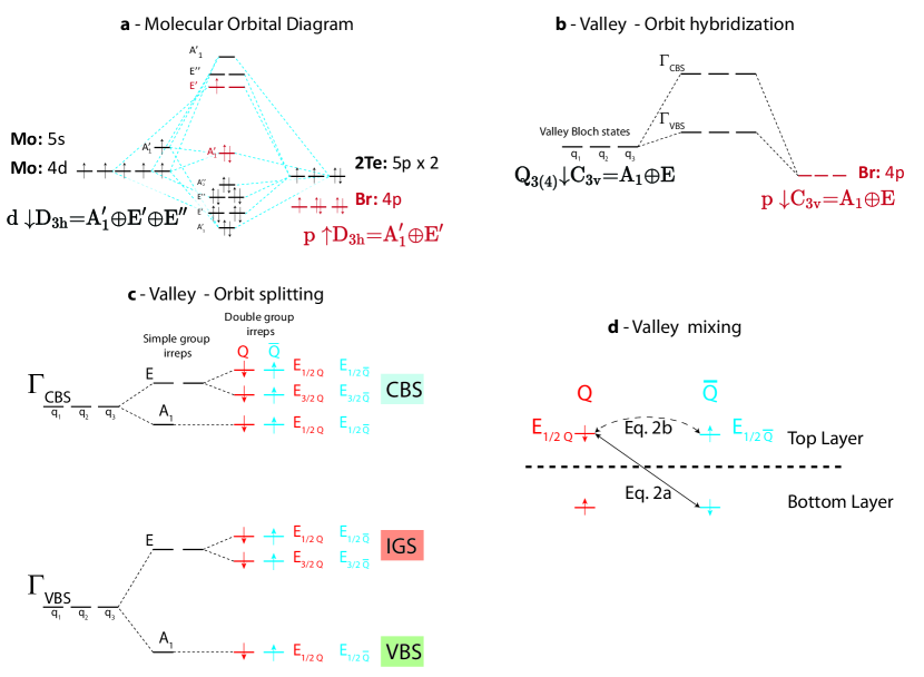
As for both the Br and substituted Te atoms the valence states arise from their p-shell, the origin of the dopant levels can be figured out from simple arguments. In TMDCs, the d-orbitals of the Mo atom restrict to the irreducible representations (irreps) , and of the D3h point group of the Mo site, . Because these irreps are also induced by the p-orbitals of the Te atom, , the d- and p-orbitals can hybridize and form bonds and bands. DFT calculations Liu2013-rm ; Kormanyos2015-bt ; Pike2017-na show that the conduction band has symmetry and the valence band has symmetry. Both bands result from anti-bonding of Te p-orbitals and Mo d-orbitals as illustrated by the molecular diagram adapted from Pike2017-na shown in Fig. 4a. The substitution of the Te atom with the Br atom will change the energy of the p-orbitals and affect both the and states. This implies that the CBS are likely formed from the originally located in the conduction band; the VBS and IGS are likely formed from the , originally located in the valence band.
Using band representations theory, a theory of irreducible representations of space groups Evarestov1986-ct , detailed in supplementary, one can show that the p-orbitals of the Te (or Br) atoms restrict to the irreps and of the C3v point-group of the Te(or Br) site, , furthermore, one can show that the Bloch states at the Q-valleys restrict to the same irreps, . This decomposition is illustrated Fig. 4b. Consequently, the hybridization of the dopant p-orbitals and the Q-valley Bloch states are allowed to hybridize with symmetries and . This is confirmed by DFT calculations Liu2013-rm ; Liu2015-ju showing that all three orbital components of the anion site have a large contribution to the Q-valleys in the conduction band. Thus, two sets (representations) of dopant levels are expected: () resulting from the p-orbitals hybridized to the Q-valleys and located near the conduction (valence band).
As originally done for shallow dopants in silicon Kohn1955-pu ; Ramdas1981-da , the Br dopant quantum states are now described on the basis of the valley Bloch states. For each star (orbit) of wavevectors and , shown in Fig. 1b, there are three non-equivalent wavevectors. Furthermore, one star has opposite spin polarization to the other one . Thus, the states can be written as:
| (1) | ||||
with Bloch wavefunctions describing the valley states where is the cell-periodic part and the envelope function describes the decay of the amplitude of the wavefunction with the Bohr radius calculated above, which describes properly the decay of the CBS as shown in Supplementary. The eigenstate should have the symmetry of the irrep of the Br site symmetry point-group C3v where the index Q or indicates from which valleys the state has been build of. Because the point-group C3v has only one and two-dimensional irreps, we expect the threefold valley degeneracy of the valley representations and to be lifted. In the case of silicon, this so-called valley-orbit splitting is of the order of few meV Zwanenburg2013-ak . Following Kohn and Luttinger Kohn1955-pu ; Ramdas1981-da , we establish the characters of the valley representations to find that each one decomposes into one symmetric state A and one doublet state E, and this for each star or . Thus, each valley representation decomposes as A1 E A1 E, as sketched in Fig. 4c. To describe spin-orbit coupling effects, we now use the double point-group C3v irreps obtained by taking the direct product of the simple point-group irreps with the spinor irrep E1/2. We find that A generates the irrep E1/2 and E generates the irreps E1/2, E3/2. As these irreps do not mix the Bloch states of the two different valleys Q and and each valley has a well defined spin polarization, the dopant-states have well-defined spin and valley-polarizations, which implies spin-valley locking. As shown in Fig. 4c, the dopant-states formed from Q-valley must be spin-down and the dopant-states formed from -valley must be spin-up. Another set of dopant-states with reversed spin-polarization, not shown in Fig.4c, must exist but they are located at higher energy due to spin-orbit splitting. Assuming an energy separation of the order of the spin-splitting of the bulk states Liu2013-rm , the two sets of dopant-states should be separated by about 250 meV for the VBS and IGS and about 15 meV for the CBS. For low temperature applications where the electron remains in the lowest energy state of the dopant, this second set of levels at higher energy can be ignored. For each irrep, using the standard operator projection method Dresselhaus2007-ed and the character table of the double point-group C3v, the coefficients are calculated to give symmetry adapted linear combinations of the valley Bloch states. Then, the spatial distribution of the probability density is calculated.
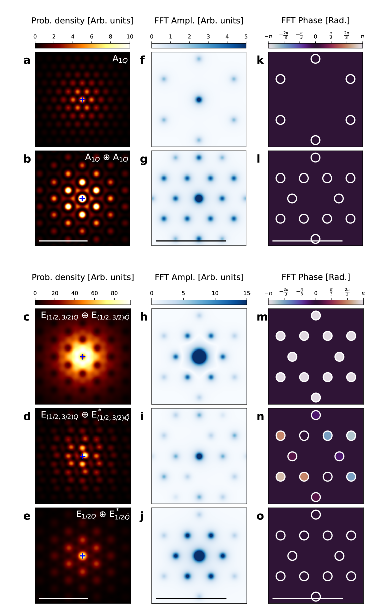
If no mixing occurs between the valleys Q and , the spatial pattern is composed of only the intra-valley Fourier components . This is illustrated Fig. 5afk for an irrep of A1Q symmetry. The spatial density map is shown Fig. 5a and the corresponding amplitude and phase of the 2D-FFT are shown Fig. 5f and Fig. 5k, respectively.
As sketched in Fig. 4d, the levels arising from the Q-valleys can be mixed with the levels arising from the -valleys in two distinct ways, either through changing the layer index with no spin-flip or, within the same layer, by changing the spin state.
For both cases, the resulting eigenstates can be written respectively as :
| (2a) | ||||
| (2b) | ||||
where is an unknown phase factor that we take as 0 or to match the experimental data. Fig. 5b shows the spatial map in presence of valley mixing, using Eq. 2a to sum two states of symmetry A1Q and A1. In addition to the intra-valley components , the Fourier map Fig. 5g shows additional components at the inter-valley components and , as observed in experimental data.
Following the symmetry of eigenstates predicted by group theory, Fig. 4c, we now plot the corresponding local DOS. Figure 5chm shows the spatial map of the probability density and the corresponding 2D-FFT resulting from the sum of four eigenstates, E1/2Q E3/2Q E1/2 E3/2, arising from and using Eq. 2a with . The result reproduces qualitatively the conductance maps of CBS, Fig. 3d. This comparison presumes that the STM spectroscopy measurements had not enough energy resolution to distinguish the states E1/2 and E3/2. Figure 5din shows the results for the sum of four eigenstates, E1/2Q E3/2Q E1/2 E3/2, now arising from and using Eq. 2b with . The result reproduces qualitatively the conductance maps of IGS, Fig. 3e. In particular, the offset of the DOS maxima with respect to the image center indicated by plus symbol. Finally, Figure 5ejo shows the results for the sum of two eigenstates, E1/2Q E1/2, also arising from and using Eq. 2b with . The result reproduces qualitatively the conductance maps of VBS, Fig. 3f. A side by side comparison of the conductance maps and calculated probability densities for the three energy ranges are shown in Supplementary.
Because of the large Bohr size, DFT calculations of the bulk Br-doped 2H-TMDC was too heavy, however, the calculation for one atomic monolayer is possible and shown in supplementary. A donor-state near the conductance band is identified and the corresponding local DOS presents a modulation resulting from the hybridization to the K-valleys, instead of the Q-valleys observed by STM in the bulk material. Furthermore, calculation of the partial density of states, Supplementary Fig. 16, shows that the orbitals of the 1st and 2nd neighbors Mo atoms have a large contribution to this donor-state. As the Bloch states at the K-point of the conduction band have character, this confirms the hybridization of the Br p-orbitals with the Bloch states at the K-valleys.
3 Conclusion
To summarize, we have identified the ESR signal of the BrTe dopant in 2H-MoTe2 and found a spin state with long-lived (nanoseconds) coherence. This relatively long coherence time is believed to be the consequence of the protection by spin-valley locking. From STM measurements, we found that the dopant-orbitals are indeed hybridized to the Q-valleys.
As discussed in Ref. Gilardoni2021-sv , in bulk materials, despite the local inversion symmetry, additional spin-scattering channels become possible. In particular, inter-layer coupling allows spin-flip without changing valley. Thus, we expect this work on bulk crystals to motivate STM and ESR studies of hydrogenic spin-valley states in doped atomic monolayer of TMDCs, where the protection afforded by spin-valley locking will reach its full potential. Our DFT calculations show indeed that the Br dopant levels in a single atomic monolayer are hybridized to the K-valleys.
4 Figures
5 Methods
5.1 Crystal growth
MoTe2 single crystals were grown by the chemical vapor transport (CVT) method using Br2 as a transport agent Levy1977-nf . Stoichiometric mixture of molybdenum and tellurium powders along with Br2 were sealed in a quartz ampoule with a length of 24 cm and diameter of 1.5 cm. The bromine vapor density was approximately 5 mg/cm3. The ampoule was pumped out to a residual pressure of 10-4 atm. and then placed into a horizontal tube furnace with a linear temperature gradient. The temperatures of the hot zone T1 and the cold zone T2 were 850 ∘C and 770 ∘C, respectively. In the hot zone, the precursor reacted with the gaseous transport agent to form volatile compounds, which, under the action of a temperature gradient, were transferred to the opposite end of the ampoule (cold zone), where MoTe2 single crystals grew and Br2 was released. The single crystal growth procedure was carried out for 500 hours, followed by slow cooling to room temperature. The crystalline structure was checked by X-ray diffraction where we found that MoTe2 crystallized in a hexagonal structure (Space group P63/mmc (#194)) with the lattice parameters a = 3.540(7) Å and c = 13.983(5) Å.
5.2 Transport measurements
Transport measurements were carried out in a Physical Property Measurement System (PPMS). The longitudinal and Hall resistance were measured using a standard lock-in technique. For these measurements, the bulk crystals were exfoliated down to obtain thin crystals about ten micrometers thick, deposited on an insulating silicon wafer. The electrical contacts were realized with gold wires () glued with silver epoxy.
5.3 Photoemission
The ARPES measurements were conducted at the CASSIOPEE beamline of Synchrotron SOLEIL (France). Before the measurement, the sample was cooled down at T 12 K and cleaved in situ in UHV in the analysis chamber. The CASSIOPEE beamline is equipped with a Scienta R4000 hemisperical electron analyzer (angular acceptance ±15∘) with vertical slits. The angular and energy resolutions were 0.25∘ and 15 meV. The mean diameter of the incident photon beam was smaller than 50 µm. We used linear horizontal polarized photons with an energy of 47 eV. Binding energies are referenced to the Fermi level of a gold foil in electrical contact with the sample.
5.4 ESR measurements
The samples were studied with two Bruker spectrometer, EMX and ELEXYS-II, working in CW-mode in X-band in a cavity of frequency 9.482 GHz. The thin flat bromine-doped 2H-MoTe2 crystal was glued on the flat part machined into a glass rod, enabling the control of the angular orientation of the sample with respect to the applied magnetic field. The angle is measured with respect to the axis perpendicular to the sample. The orientation was manually controlled with a goniometer of 0.5 deg precision. The spectrometer provides the first derivative of the absorbed microwave power as a function of magnetic field. Measurements were carried out in a helium-flow cryostat in the temperature range from T = 4 K to T = 300 K. Changing the in-plane orientation did not lead to significant changes in the spectrum and so the in-plane orientation has not been determined.
5.5 STM measurements
The bulk 2H-MoTe2 doped crystals were cleaved under UHV conditions, P mbar, to get clean surfaces free of atomic contamination. The samples were measured at T = 77 K in two different microscopes: one Joule-Thomson (JT) from SPECS and one LT from Omicron (Scienta). The differential conductance spectra are taken with the feedback loop open with current setpoint set at sample bias of -1.2 V. To compare spectra measured at different locations or plotting conductance maps, we need to remove the effects of changing tunnel barrier height. To that end, we assume that the total DOS is conserved on the energy range [-1.2 V, 0.15 V ]. Thus, we normalize all measured curves by their integrated values .
Availability of data and materials
Any further data are available from the corresponding author upon request.
Code availability
Most of data analysis and plotting were done under python, expect for the analysis of ESR data which were done with Matlab code (Easy spin). All codes are available upon request.
Acknowledgments
We acknowledge financial support from ANR MECHASPIN Grant No. ANR-17-CE24-0024-02 and ANR FRONTAL Grant No. ANR-19-CE09-0017-02. We acknowledge support from the CNRS research infrastructure RENARD (FR 3443) for EPR facilities. The crystal growth was carried out within the state assignment of Ministry of Science and Higher Education of the Russian Federation (theme “Spin” No. 122021000036-3). The computational support from the Technical University of Dresden computing cluster (TAURUS), from High Performance Computing Center (HLRS) in Stuttgart, Germany is gratefully appreciated. We acknowledge useful discussions regarding samples with Dr. B. Fauqué. We thank Pr. H. Dery, Dr. CM. Gilardoni and Pr. M. Guimaraes for careful reading of the manuscript and suggestions.
Authors’ contributions
H.A. proposed the project. V.M., S.M and A.P. grew the MoTe2 crystal. V.Sh., G.L. H.A. and J.L.C. realized the ESR measurements. V.Sh., H.A. and B.L. realized the transport measurements. D.P and A.O. realized the ARPES measurements. V.Sh., V.St., H.A., J.C.G, G.R., C.D., L.R.S., realized the STM measurements. M.G.A. and A.V.K. performed the DFT calculations. V.Sh. and H.A. realized the group theory analysis and wrote the paper with contributions of all authors.
Conflict of interest/Competing interests
The authors declare no competing interests.
Declarations
Supplementary information The online version contains supplementary material available at .. \bmheadCorrespondence and requests for materials should be addressed to H.A.
References
- \bibcommenthead
- (1) Zwanenburg, F.A., Dzurak, A.S., Morello, A., Simmons, M.Y., Hollenberg, L.C.L., Klimeck, G., Rogge, S., Coppersmith, S.N., Eriksson, M.A.: Silicon quantum electronics. Rev. Mod. Phys. 85(3), 961–1019 (2013)
- (2) Salfi, J., Mol, J.A., Rahman, R., Klimeck, G., Simmons, M.Y., Hollenberg, L.C.L., Rogge, S.: Spatially resolving valley quantum interference of a donor in silicon. Nat. Mater. 13(6), 605–610 (2014)
- (3) Usman, M., Bocquel, J., Salfi, J., Voisin, B., Tankasala, A., Rahman, R., Simmons, M.Y., Rogge, S., Hollenberg, L.C.L.: Spatial metrology of dopants in silicon with exact lattice site precision. Nat. Nanotechnol. 11(9), 763–768 (2016)
- (4) Voisin, B., Bocquel, J., Tankasala, A., Usman, M., Salfi, J., Rahman, R., Simmons, M.Y., Hollenberg, L.C.L., Rogge, S.: Valley interference and spin exchange at the atomic scale in silicon. Nat. Commun. 11(1), 6124 (2020)
- (5) Zhu, Z.Y., Cheng, Y.C., Schwingenschlögl, U.: Giant spin-orbit-induced spin splitting in two-dimensional transition-metal dichalcogenide semiconductors. Phys. Rev. B Condens. Matter 84(15), 153402 (2011)
- (6) Xiao, D., Liu, G.-B., Feng, W., Xu, X., Yao, W.: Coupled spin and valley physics in monolayers of MoS_{2} and other Group-VI dichalcogenides. Phys. Rev. Lett. 108(19), 196802 (2012)
- (7) Kośmider, K., González, J.W., Fernández-Rossier, J.: Large spin splitting in the conduction band of transition metal dichalcogenide monolayers. Phys. Rev. B Condens. Matter 88(24), 245436 (2013)
- (8) Liu, G.-B., Shan, W.-Y., Yao, Y., Yao, W., Xiao, D.: Three-band tight-binding model for monolayers of group-VIB transition metal dichalcogenides. Phys. Rev. B Condens. Matter 88(8), 085433 (2013)
- (9) Roldán, R., López-Sancho, M.P., Guinea, F., Cappelluti, E., Silva-Guillén, J.A., Ordejón, P.: Momentum dependence of spin–orbit interaction effects in single-layer and multi-layer transition metal dichalcogenides. 2D Mater. 1(3), 034003 (2014)
- (10) Liu, G.-B., Xiao, D., Yao, Y., Xu, X., Yao, W.: Electronic structures and theoretical modelling of two-dimensional group-VIB transition metal dichalcogenides. Chem. Soc. Rev. 44(9), 2643–2663 (2015)
- (11) Kormányos, A., Burkard, G., Gmitra, M., Fabian, J., Zólyomi, V., Drummond, N.D., Fal’ko, V.: k.p theory for two-dimensional transition metal dichalcogenide semiconductors. 2D Mater. 2(2), 022001 (2015)
- (12) Rohling, N., Burkard, G.: Universal quantum computing with spin and valley states. New J. Phys. 14(8), 083008 (2012)
- (13) Kormányos, A., Zólyomi, V., Drummond, N.D., Burkard, G.: Spin-Orbit coupling, quantum dots, and qubits in monolayer transition metal dichalcogenides. Phys. Rev. X 4(1), 011034 (2014)
- (14) Wu, Y., Tong, Q., Liu, G.-B., Yu, H., Yao, W.: Spin-valley qubit in nanostructures of monolayer semiconductors: Optical control and hyperfine interaction. Phys. Rev. B Condens. Matter 93(4), 045313 (2016)
- (15) Pearce, A.J., Burkard, G.: Electron spin relaxation in a transition-metal dichalcogenide quantum dot. 2D Mater. 4(2), 025114 (2017)
- (16) Széchenyi, G., Chirolli, L., Pályi, A.: Impurity-assisted electric control of spin-valley qubits in monolayer MoS2. 2D Mater. 5(3), 035004 (2018)
- (17) David, A., Burkard, G., Kormányos, A.: Effective theory of monolayer TMDC double quantum dots. 2D Mater. 5(3), 035031 (2018)
- (18) Pawłowski, J., Żebrowski, D., Bednarek, S.: Valley qubit in a gated MoS2 monolayer quantum dot. Phys. Rev. B Condens. Matter 97(15), 155412 (2018)
- (19) Wu, F., Lovorn, T., Tutuc, E., MacDonald, A.H.: Hubbard model physics in transition metal dichalcogenide moiré bands. Phys. Rev. Lett. 121(2), 026402 (2018)
- (20) Schrade, C., Fu, L.: Spin-valley density wave in moir\’e materials. Phys. Rev. B Condens. Matter 100(3), 035413 (2019)
- (21) Wu, F., Lovorn, T., Tutuc, E., Martin, I., MacDonald, A.H.: Topological insulators in twisted transition metal dichalcogenide homobilayers. Phys. Rev. Lett. 122(8), 086402 (2019)
- (22) Wang, L., Shih, E.-M., Ghiotto, A., Xian, L., Rhodes, D.A., Tan, C., Claassen, M., Kennes, D.M., Bai, Y., Kim, B., Watanabe, K., Taniguchi, T., Zhu, X., Hone, J., Rubio, A., Pasupathy, A.N., Dean, C.R.: Correlated electronic phases in twisted bilayer transition metal dichalcogenides. Nat. Mater. 19(8), 861–866 (2020)
- (23) Tang, Y., Li, L., Li, T., Xu, Y., Liu, S., Barmak, K., Watanabe, K., Taniguchi, T., MacDonald, A.H., Shan, J., Mak, K.F.: Simulation of hubbard model physics in WSe2/WS2 moiré superlattices. Nature 579(7799), 353–358 (2020)
- (24) Regan, E.C., Wang, D., Jin, C., Bakti Utama, M.I., Gao, B., Wei, X., Zhao, S., Zhao, W., Zhang, Z., Yumigeta, K., Blei, M., Carlström, J.D., Watanabe, K., Taniguchi, T., Tongay, S., Crommie, M., Zettl, A., Wang, F.: Mott and generalized wigner crystal states in WSe2/WS2 moiré superlattices. Nature 579(7799), 359–363 (2020)
- (25) Li, T., Jiang, S., Li, L., Zhang, Y., Kang, K., Zhu, J., Watanabe, K., Taniguchi, T., Chowdhury, D., Fu, L., Shan, J., Mak, K.F.: Continuous mott transition in semiconductor moiré superlattices. Nature 597(7876), 350–354 (2021)
- (26) Li, H., Li, S., Regan, E.C., Wang, D., Zhao, W., Kahn, S., Yumigeta, K., Blei, M., Taniguchi, T., Watanabe, K., Tongay, S., Zettl, A., Crommie, M.F., Wang, F.: Imaging two-dimensional generalized wigner crystals. Nature 597(7878), 650–654 (2021)
- (27) Song, Y., Dery, H.: Transport theory of monolayer transition-metal dichalcogenides through symmetry. Phys. Rev. Lett. 111(2), 026601 (2013)
- (28) Gilardoni, C.M., Hendriks, F., van der Wal, C.H., Guimarães, M.H.D.: Symmetry and control of spin-scattering processes in two-dimensional transition metal dichalcogenides. Phys. Rev. B Condens. Matter 103(11), 115410 (2021)
- (29) Yang, L., Sinitsyn, N.A., Chen, W., Yuan, J., Zhang, J., Lou, J., Crooker, S.A.: Long-lived nanosecond spin relaxation and spin coherence of electrons in monolayer MoS 2 and WS 2. Nat. Phys. 11(10), 830–834 (2015)
- (30) Ersfeld, M., Volmer, F., de Melo, P.M.M.C., de Winter, R., Heithoff, M., Zanolli, Z., Stampfer, C., Verstraete, M.J., Beschoten, B.: Spin states protected from intrinsic Electron–Phonon coupling reaching 100 ns lifetime at room temperature in MoSe2. Nano Lett. 19(6), 4083–4090 (2019)
- (31) Yang, L., Chen, W., McCreary, K.M., Jonker, B.T., Lou, J., Crooker, S.A.: Spin coherence and dephasing of localized electrons in monolayer MoS. Nano Lett. 15(12), 8250–8254 (2015)
- (32) Jiang, M., Wu, Z., Yang, Q., Zhang, Y., Men, Y., Jia, T., Sun, Z., Feng, D.: Coherent spin dynamics of localized electrons in monolayer MoS2. J. Phys. Chem. Lett. 13(11), 2661–2667 (2022)
- (33) Dey, P., Yang, L., Robert, C., Wang, G., Urbaszek, B., Marie, X., Crooker, S.A.: Gate-Controlled Spin-Valley locking of resident carriers in WSe_{2} monolayers. Phys. Rev. Lett. 119(13), 137401 (2017)
- (34) Evarestov, R.A., Smirnov, V.P.: Application of band representations of space groups in the theory of phase transitions and point defects in crystals. Phys. Status Solidi B Basic Res. 136(2), 409–415 (1986)
- (35) Liu, G.-B., Pang, H., Yao, Y., Yao, W.: Intervalley coupling by quantum dot confinement potentials in monolayer transition metal dichalcogenides. New J. Phys. 16(10), 105011 (2014)
- (36) Kaasbjerg, K., Martiny, J.H.J., Low, T., Jauho, A.-P.: Symmetry-forbidden intervalley scattering by atomic defects in monolayer transition-metal dichalcogenides. Phys. Rev. B Condens. Matter 96(24), 241411 (2017)
- (37) Komsa, H.-P., Kotakoski, J., Kurasch, S., Lehtinen, O., Kaiser, U., Krasheninnikov, A.V.: Two-dimensional transition metal dichalcogenides under electron irradiation: defect production and doping. Phys. Rev. Lett. 109(3), 035503 (2012)
- (38) Dolui, K., Rungger, I., Das Pemmaraju, C., Sanvito, S.: Possible doping strategies for MoS_{2} monolayers: An ab initio study. Phys. Rev. B: Condens. Matter Mater. Phys. 88(7), 075420 (2013)
- (39) Guo, S., Wang, Y., Wang, C., Tang, Z., Zhang, J.: Large spin-orbit splitting in the conduction band of halogen (f, cl, br, and i) doped monolayer WS2 with spin-orbit coupling. Phys. Rev. B Condens. Matter 96(24), 245305 (2017)
- (40) Onofrio, N., Guzman, D., Strachan, A.: Novel doping alternatives for single-layer transition metal dichalcogenides. J. Appl. Phys. 122(18), 185102 (2017)
- (41) Morsli, M., Bonnet, A., Jousseaume, V., Cattin, L., Conan, A., Zoaeter, M.: Tellurium depletion electrical effects in MoTe2-x single crystals doped with bromine. J. Mater. Sci. 32(9), 2445–2449 (1997)
- (42) Zhang, X., Liu, Q., Luo, J.-W., Freeman, A.J., Zunger, A.: Hidden spin polarization in inversion-symmetric bulk crystals. Nat. Phys. 10, 387 (2014)
- (43) Riley, J.M., Mazzola, F., Dendzik, M., Michiardi, M., Takayama, T., Bawden, L., Granerød, C., Leandersson, M., Balasubramanian, T., Hoesch, M., Kim, T.K., Takagi, H., Meevasana, W., Hofmann, P., Bahramy, M.S., Wells, J.W., King, P.D.C.: Direct observation of spin-polarized bulk bands in an inversion-symmetric semiconductor. Nat. Phys. 10(11), 835–839 (2014)
- (44) Razzoli, E., Jaouen, T., Mottas, M.-L., Hildebrand, B., Monney, G., Pisoni, A., Muff, S., Fanciulli, M., Plumb, N.C., Rogalev, V.A., Strocov, V.N., Mesot, J., Shi, M., Dil, J.H., Beck, H., Aebi, P.: Selective probing of hidden Spin-Polarized states in Inversion-Symmetric bulk MoS_{2}. Phys. Rev. Lett. 118(8), 086402 (2017)
- (45) Tu, J., Chen, X.B., Ruan, X.Z., Zhao, Y.F., Xu, H.F., Chen, Z.D., Zhang, X.Q., Zhang, X.W., Wu, J., He, L., Zhang, Y., Zhang, R., Xu, Y.B.: Direct observation of hidden spin polarization in 2H-MoTe2. Phys. Rev. B Condens. Matter 101(3) (2020)
- (46) Cho, S., Park, J.-H., Hong, J., Jung, J., Kim, B.S., Han, G., Kyung, W., Kim, Y., Mo, S.-K., Denlinger, J.D., Shim, J.H., Han, J.H., Kim, C., Park, S.R.: Experimental observation of hidden berry curvature in inversion-symmetric bulk 2H-WSe2. Phys. Rev. Lett. 121(18) (2018)
- (47) Beaulieu, S., Schusser, J., Dong, S., Schüler, M., Pincelli, T., Dendzik, M., Maklar, J., Neef, A., Ebert, H., Hricovini, K., Wolf, M., Braun, J., Rettig, L., Minár, J., Ernstorfer, R.: Revealing hidden orbital pseudospin texture with Time-Reversal dichroism in photoelectron angular distributions. Phys. Rev. Lett. 125(21), 216404 (2020)
- (48) Han, T.T., Chen, L., Cai, C., Wang, Z.G., Wang, Y.D., Xin, Z.M., Zhang, Y.: Metal-Insulator transition and emergent gapped phase in the Surface-Doped 2D semiconductor 2H-MoTe_{2}. Phys. Rev. Lett. 126(10), 106602 (2021)
- (49) Grasso, V., Mondio, G., Saitta, G.: Optical constants of MoTe2 from reflectivity measurements. (brillouin zone transitions). J. Phys. C: Solid State Phys. 5(10), 1101 (1972)
- (50) Shklovskii, B.I., Efros, A.: Electronic Properties of Doped Semiconductors, p. 388. Springer, ??? (1984)
- (51) Guguchia, Z., Kerelsky, A., Edelberg, D., Banerjee, S., von Rohr, F., Scullion, D., Augustin, M., Scully, M., Rhodes, D.A., Shermadini, Z., Luetkens, H., Shengelaya, A., Baines, C., Morenzoni, E., Amato, A., Hone, J.C., Khasanov, R., Billinge, S.J.L., Santos, E., Pasupathy, A.N., Uemura, Y.J.: Magnetism in semiconducting molybdenum dichalcogenides. Sci Adv 4(12), 3672 (2018)
- (52) Title, R.S., Shafer, M.W.: Electron-Paramagnetic-Resonance studies on arsenic acceptors in natural (2h) and synthetic (3r) MoS2 crystals. Phys. Rev. B Condens. Matter 8(2), 615–620 (1973)
- (53) Stesmans, A., Iacovo, S., Afanas’ev, V.V.: ESR study of p-type natural 2h-polytype MoS2 crystals: The as acceptor activity. Appl. Phys. Lett. 109(17), 172104 (2016)
- (54) Toledo, J.R., de Oliveira, R., Vaz, P.H., Brandão, F.D., Ribeiro, G.M., González, J.C., Krambrock, K.: Electrical and structural characterization of shallow as acceptors in natural p-type 2H-MoS2. Appl. Phys. Lett. 114(19), 192103 (2019)
- (55) Poole, C.P.: Electron Spin Resonance: A Comprehensive Treatise on Experimental Techniques. Courier Corporation, ??? (1996)
- (56) Meier, F., Zakharchenya, B.P.: Optical Orientation. Elsevier, ??? (2012)
- (57) Wang, G., Chernikov, A., Glazov, M.M., Heinz, T.F., Marie, X., Amand, T., Urbaszek, B.: Colloquium: Excitons in atomically thin transition metal dichalcogenides. Rev. Mod. Phys. 90(2), 021001 (2018)
- (58) Edelberg, D., Rhodes, D., Kerelsky, A., Kim, B., Wang, J., Zangiabadi, A., Kim, C., Abhinandan, A., Ardelean, J., Scully, M., Scullion, D., Embon, L., Zu, R., Santos, E.J.G., Balicas, L., Marianetti, C., Barmak, K., Zhu, X., Hone, J., Pasupathy, A.N.: Approaching the intrinsic limit in transition metal diselenides via point defect control. Nano Lett. 19(7), 4371–4379 (2019)
- (59) González, C., Biel, B., Dappe, Y.J.: Theoretical characterisation of point defects on a MoS2 monolayer by scanning tunnelling microscopy. Nanotechnology 27(10), 105702 (2016)
- (60) Roushan, P., Seo, J., Parker, C.V., Hor, Y.S., Hsieh, D., Qian, D., Richardella, A., Hasan, M.Z., Cava, R.J., Yazdani, A.: Topological surface states protected from backscattering by chiral spin texture. Nature 460(7259), 1106–1109 (2009)
- (61) Liu, H., Chen, J., Yu, H., Yang, F., Jiao, L., Liu, G.-B., Ho, W., Gao, C., Jia, J., Yao, W., Xie, M.: Observation of intervalley quantum interference in epitaxial monolayer tungsten diselenide. Nat. Commun. 6, 8180 (2015)
- (62) Kohn, W., Luttinger, J.M.: Theory of donor states in silicon. Phys. Rev. 98(4), 915–922 (1955)
- (63) Ramdas, A.K., Rodriguez, S.: Spectroscopy of the solid-state analogues of the hydrogen atom: donors and acceptors in semiconductors. Rep. Prog. Phys. 44(12), 1297 (1981)
- (64) Pike, N.A., Van Troeye, B., Dewandre, A., Petretto, G., Gonze, X., Rignanese, G.-M., Verstraete, M.J.: Origin of the counterintuitive dynamic charge in the transition metal dichalcogenides. Phys. Rev. B Condens. Matter 95(20), 201106 (2017)
- (65) Dresselhaus, M.S., Dresselhaus, G., Jorio, A.: Group Theory: Application to the Physics of Condensed Matter. Springer, ??? (2007)
- (66) Jain, A., Ong, S.P., Hautier, G., Chen, W., Richards, W.D., Dacek, S., Cholia, S., Gunter, D., Skinner, D., Ceder, G., Persson, K.A.: Commentary: The materials project: A materials genome approach to accelerating materials innovation. APL Materials 1(1), 011002 (2013)
- (67) Lévy, F.: Single-crystal growth of layered crystals. Il Nuovo Cimento B (1971-1996) 38(2), 359–368 (1977)
See pages - of MoTe_2_Br_SI.pdf