Design and Optimization of Magnetic-core Solenoid Inductor for Multi-phase Buck Converter
Metal Inter-layer Via Keep-out-zone in M3D IC: A Critical Process-aware Design Consideration (Accepted in ISQED 2023)
Abstract
Metal inter-layer via (MIV) in Monolithic three-dimensional integrated circuits (M3D-IC) is used to connect inter-layer devices and provide power and clock signals across multiple layers. The size of MIV is comparable to logic gates because of the significant reduction in substrate layers due to sequential integration. Despite MIV’s small size, the impact of MIV on the performance of adjacent devices should be considered to implement IC designs in M3D-IC technology. In this work, we systematically study the changes in performance of transistors when they are placed near MIV to understand the effect of MIV on adjacent devices when MIV passes through the substrate. Simulation results suggest that the keep-out-zone (KOZ) for MIV should be considered to ensure the reliability of M3D-IC technology and this KOZ is highly dependent on the M3D-IC process. In this paper, we show that the transistor placed near MIV considering the M1 metal pitch as the separation will have up to increase in leakage current, when the channel doping is , source/drain doping of and substrate layer height of . We also show that, this increase in leakage current can also be reduced significantly by having KOZ around MIV, which is dependent on the process.
I Introduction
Monolithic three-dimensional integrated circuit (M3D-IC) technology offers a promising solution to meet future computational needs. The need for M3D-IC technology arises since the conventional 2D-IC technology is limited by lithography and power constraints, whereas conventional three-dimensional integrated circuit (3D-IC) technology enabled by die stacking is limited by the through-silicon-via (TSV) size [1, 2, 3, 4]. The substrate layers in M3D-IC technology are realized by sequential integration. These layers are connected by metal inter-layer via (MIV), which are of the same size as logic gates [5]. This reduction in MIV size compared to the TSV has become possible by reduction in via height through sequential integration. However, to ensure the stability of the devices at the bottom layer, the top layers of M3D-IC should be processed below 5000 C [6, 7, 8, 9] which limits the M3D-IC process such as doping concentrations.
MIVs are realized by metal surrounding oxide to provide electrical insulation to the substrate. However, this realization also forms metal-insulator-semiconductor (MIS) structure, and hence MIV can affect the substrate region around it [10, 11]. Therefore, the impact of MIV on the transistors around it should be studied to ensure the reliability of M3D-IC implementations. To the best of authors’ knowledge, there are no commercial ICs with the defined M3D-IC process specifically doping concentration of top layers, substrate layer height and MIV thickness. Therefore, the process parameters for the IC design should be considered to understand the MIV impact on the devices around it.
In this work, we systematically studied the impact of MIV on the adjacent devices and the simulation results suggest that the transistor placed near MIV considering the M1 metal pitch as the separation will have up to increase in leakage current specifically when the channel doping is , source/drain doping of and substrate layer height of . This impact can be reduced by increasing the keep-out-zone (KOZ) for MIV and this KOZ is highly dependent on the process parameters of M3D-IC technology. Therefore, process-aware KOZ is required to ensure the reliability of M3D-IC design.
The organization of the rest of the paper is as follows: Section II discusses about the background and previous works on M3D-IC technology and the motivation of this work. Section III demonstrates the impact of MIV on different transistor placement scenarios. Section IV investigates the process parameters influence on the transistor operation when MIV is placed at M1 metal pitch separation to the transistor. Section V discusses the need for process-aware Keep-out-zone (KOZ) for the MIV, and KOZ values for different process parameters are presented. Section VI brings up the future directions for current work. The concluding remarks are given in Section VII.
II Background and Motivation
In M3D-IC technology, the top-layer devices should be processed sequentially under low-temperatures i.e., less than C to ensure the quality of bottom-layer devices [6, 7, 8, 9]. With this sequential integration, the substrate layers are thinned down below 100nm thickness using layer transfer process [12]. With thin substrate and thin inter-layer dielectric (ILD), the metal inter-layer via (MIV) that connects devices at two different layers has the height of 100nm – 500nm. This reduction in height helps us to reduce the MIV thickness significantly thus allowing high MIV density () [13]. Recent works from CEA-LETI focus on sequential layer integration at lower temperatures and measured the device characteristics on both top and bottom layers with different integration techniques specifically Fully Depleted Silicon On Insulator (FDSOI) transistors [14, 15]. Several works on the M3D integration focuses on the partitioning, placement and routing in Monolithic 3D integration considering different top-layer device technology specifically bulk [16, 17] or FDSOI [18, 15]. Monolithic 3D-FPGA is designed using thin-film-transistors (TFT) in the lop layer [19]. [20] have used the unique structure of recessed-channel-transistors in top layer to study its performance. Some M3D-IC based open libraries are available currently. [16, 17] use conventional CMOS technology to present 45nm library for M3D integration. [18] have studied the power benefit of M3D-IC using FinFET based 7nm technology node. Although several demonstrations of M3D-IC process are performed, there are no existing commercial industry standards [21].
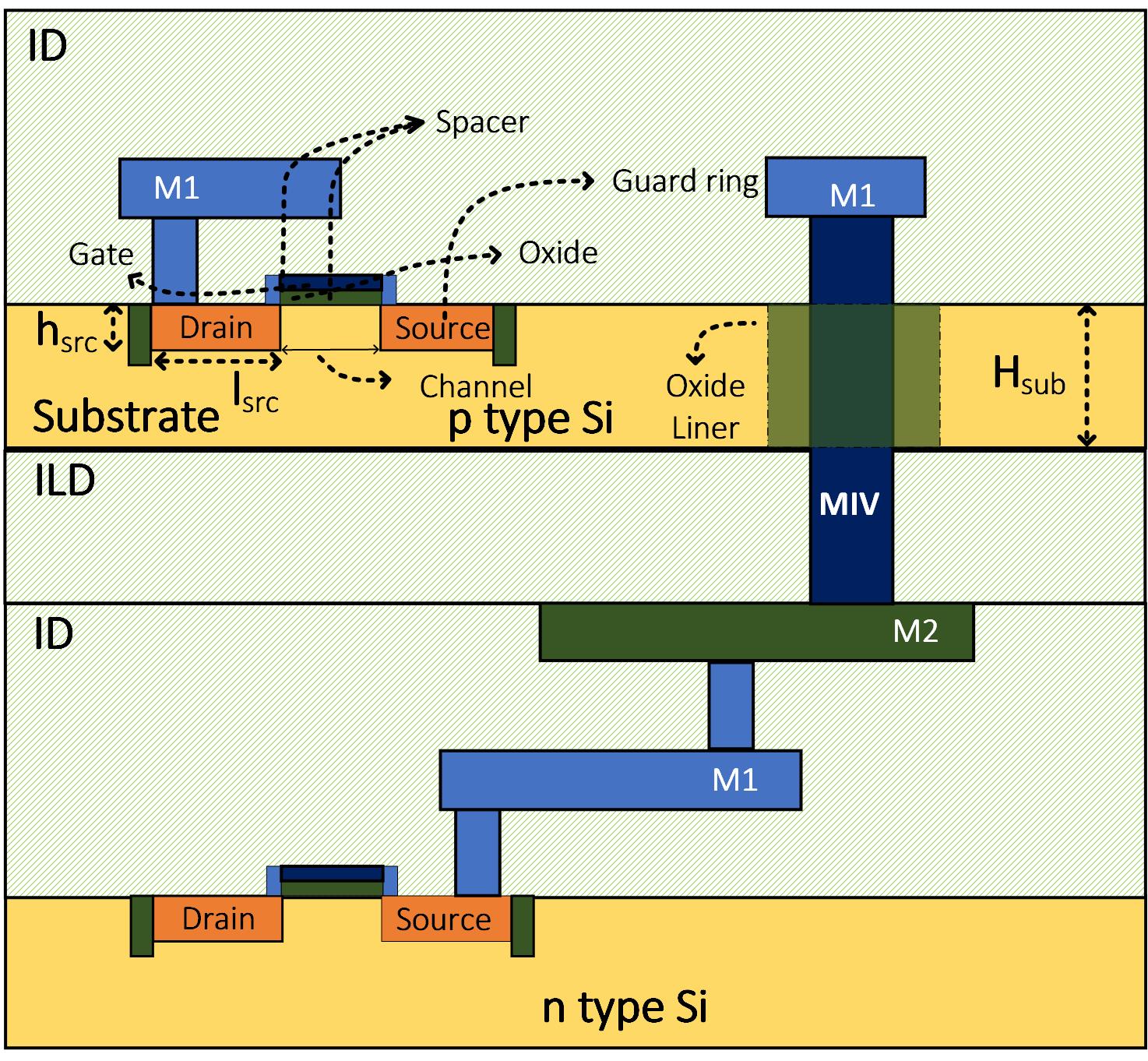
In this work, we focus on the SOI devices on the top layer with thin substrate layer of up to 100 nm thickness as suggested by previous works [12]. One of the major benefit of M3D-IC technology is to allow heterogeneous integration. This M3D-IC process will also consider the substrate biasing at the top-tier and hence tuning the threshold voltage of the transistor for analog and digital applications similar to the conventional MOSFET. The two-layer M3D process assumed in this work is shown in Figure 1. With this consideration, the MIV passes through the substrate and essentially forms a metal-insulator-semiconductor (MIS) structure. Therefore, the impact of MIV on the adjacent devices should be studied since this MIS structure can interact through the substrate region around it. The rest of the paper will systematically study the impact of MIV on the adjacent devices considering the orientation of the channel with respect to the MIV.
III MIV Effect on Transistor Operation
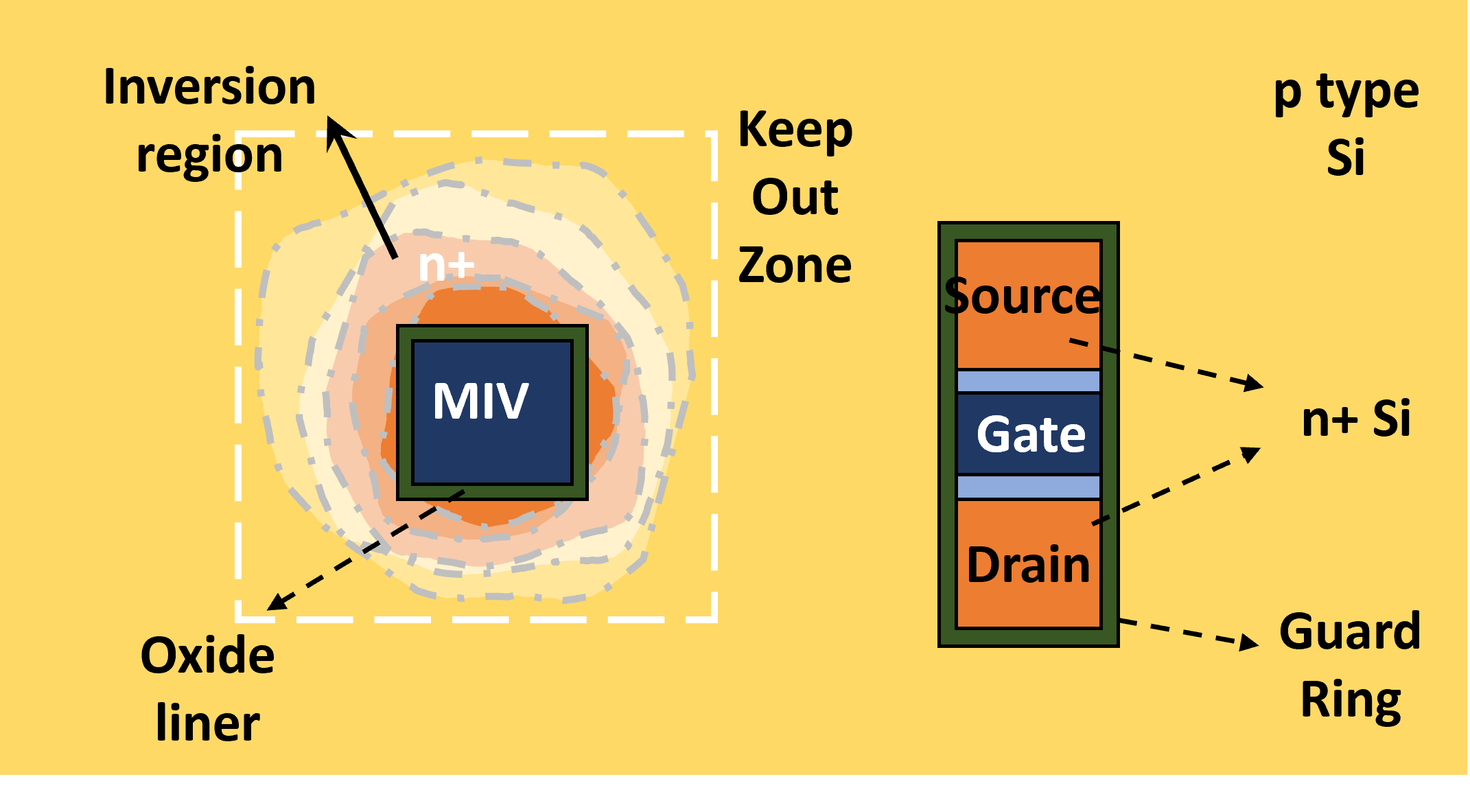
MIV with substrate around it forms a metal-insulator-semiconductor (MIS) structure, and essentially works like a MOS capacitor [10, 11]. If there is a p-type substrate region around MIV then it can be inverted (or form an n-type region) when carrying high voltage. This effect of MIV is shown in Figure 2, where the substrate around MIV will become n-type region if a higher voltage is applied to the MIV because of the MIS structure. The extent of this inversion region depends on the voltage of MIV and the M3D-IC process. If there is an n-type transistor placed near MIV, then this effect should be considered since there is a possibility of forming resistive region between source and drain, or source/drain and MIV. Therefore, an n-type transistor placed near MIV can have significant impact on its characteristics.
In this section, we study the MIV affect on transistor operation by systematically investigating two scenarios of MIV placement with respect to the transistor and is as follows:
-
1.
Vertical placement – MIV is placed parallel to the transistor as shown in Figure 3.
-
2.
Horizontal placement – MIV is placed beside the transistor as shown in Figure 7.
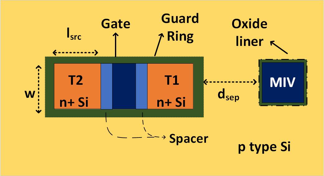
These scenarios are modeled using Sentaurus Technology Computer Aided Design (TCAD) software. We used Boron (B) as p-type substrate material, where carrier behavior is modeled with Shockley-Read-Hall (SRH) recombination model and Fermi-based statistics. The source/drain regions of the transistor is doped with Arsenic (As) (n-type) material using Gaussian profile concentration. The substrate terminal is formed with a highly doped p+ region on the substrate to provide substrate biasing. Although, not shown in the figure, the substrate contact is placed near the transistor.
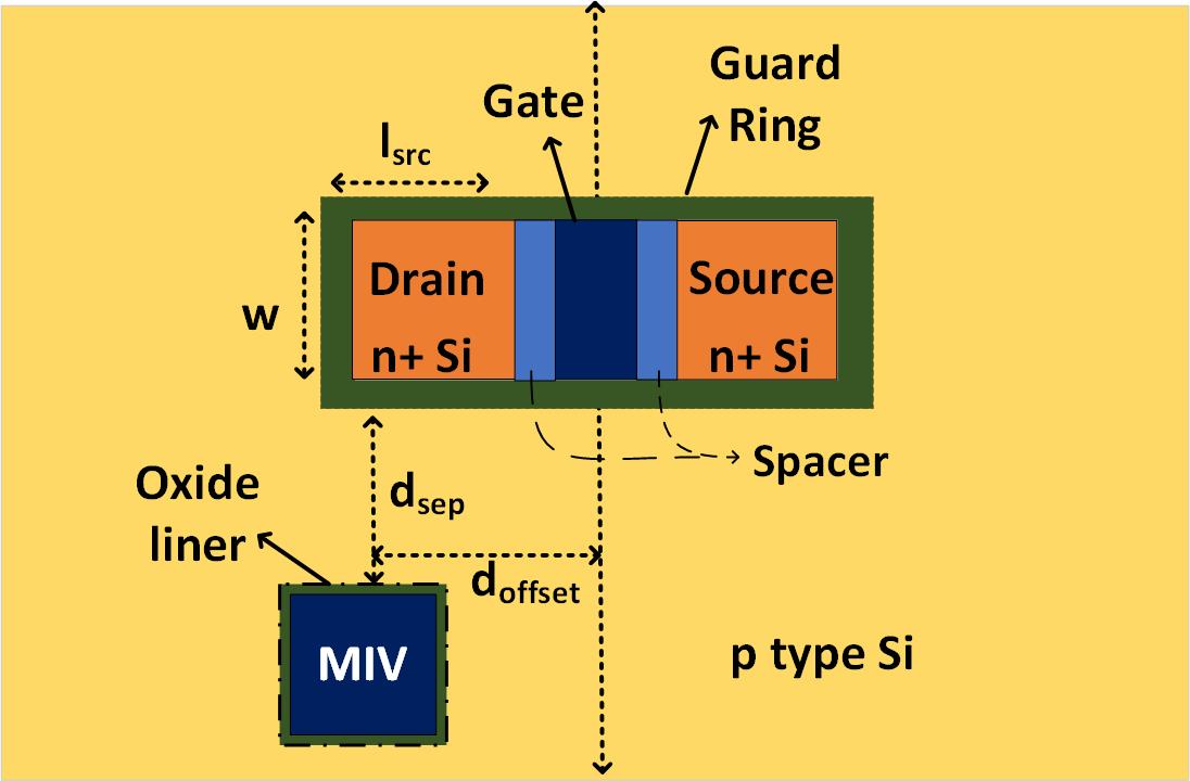
The process parameters with their nominal values and range considered for this paper is given in Table I. We considered Copper (Cu) as the interconnect metal for MIV, Silicon (Si) the substrate material and Silicon dioxide (SiO2) as the liner material. is the thickness of MIV, is the thickness of oxide liner to provide insulation from the substrate, is the height of the substrate layer through which the MIV passes through, is the substrate doping concentration, and is the source and drain doping concentrations of the transistor. The nominal value of is assumed to be 50 as discussed in the previous works [22]. The nominal value of is assumed to be considering the scaling between the TSV to MIV as discussed in [23, 24]. The length () and depth (not shown in figure) of the source/drain regions to implement the transistor is assumed to be and respectively. The width () of the transistor is assumed to be . The length of the channel is assumed to be , and the thickness of gate oxide is assumed to be 1 . The thickness and depth of guard ring are assumed to be and . The MIV pitch is assumed to be [25].
We consider two performance metrics of the transistor to study the impact of MIV:
-
1.
Maximum drain current (), which is at and .
-
2.
Maximum drain leak current (), which is at and .
We also assume that the voltage on the MIV () since it inverts the region around MIV (to n-type) due to MIS structure.
In this section, we assume the nominal values for process parameters and the only variable considered is the placement of MIV with respect to transistor.
| Parameter | Description | Value | Range |
|---|---|---|---|
| tmiv () | MIV thickness | ||
| tox () | Liner thickness | ||
| Hsub () | Substrate height | ||
| nsub () | Substrate doping | ||
| nsrc () | Source / Drain doping |
III-A Scenario 1 – Vertical placement of MIV
In this scenario, MIV is placed in parallel to the transistor channel as shown in figure 3. In this subsection, we first focus on the effect of MIV on the transistor characteristics, when channel and MIV centers are aligned. Second, we study the impact of the offset distance from transistor channel to the center of MIV () on the transistor performance. Finally, the transistor performance will be analyzed when the distance between the MIV and the transistor () is varied.
III-A1 MIV affect on transistor characteristics when channel center and MIV center are aligned
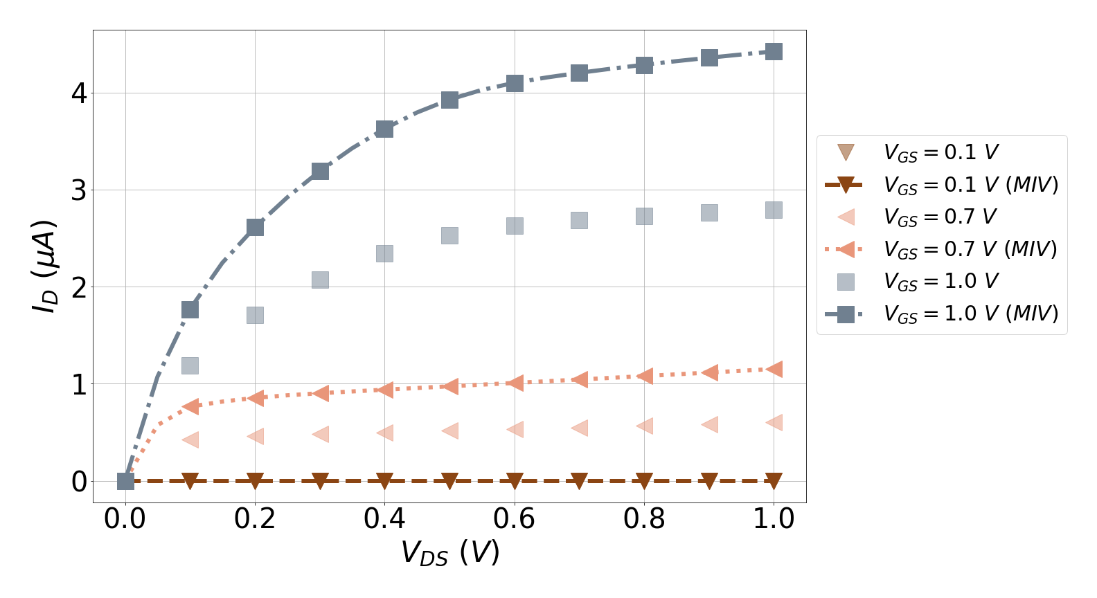
The impact of MIV on the transistor characteristics when and is shown in Figure 4. The drain current v.s. gate-source voltage plots for different drain-source voltage along with the ideal case where there is no MIV is shown in Figure 4(a). Similarly, v.s. for different is shown in Figure 4(b). From the figure, we see that the increases by up to and increases by . The increase of by is a major concern since it will affect the power and thermal reliability of the IC.
III-A2 doffset affect on transistor
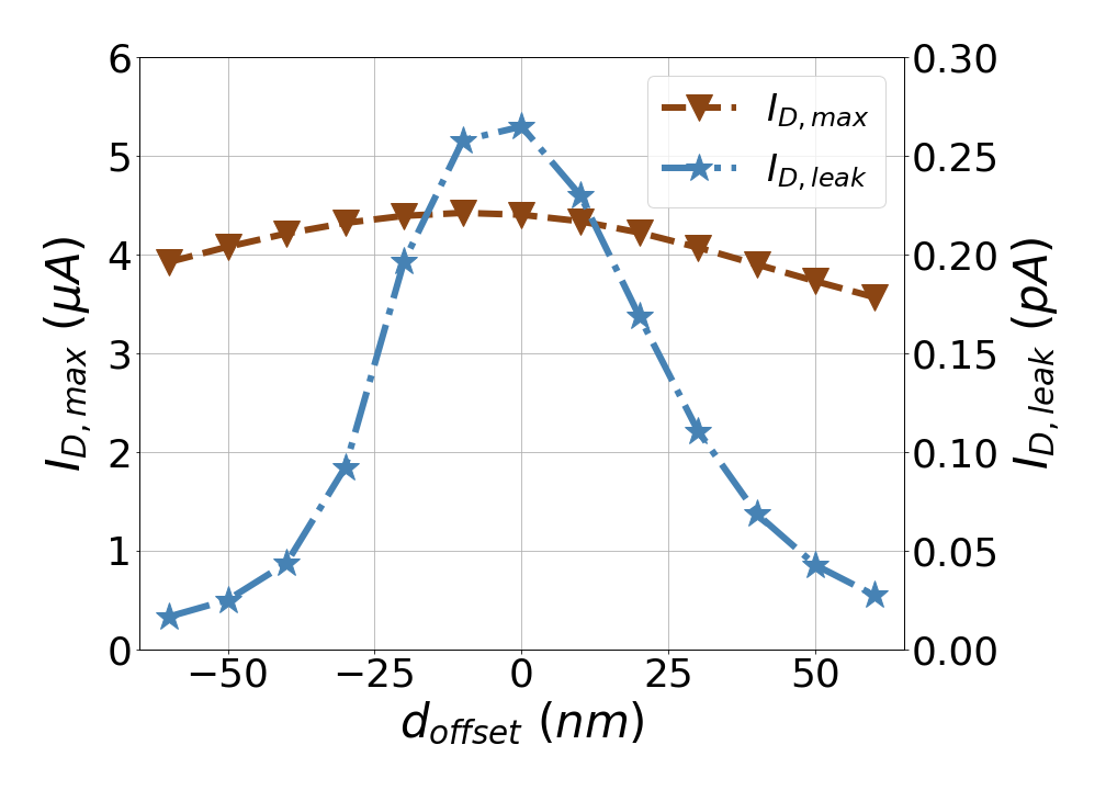
The and v.s. when is shown in Figure 5, where the at increased compared with the of transistor without MIV. The is maximum at and is increased by compared with transistor without MIV. Similarly is maximum when is low and is about compared with the transistor without MIV. This is reduced to when is high. Therefore, placing MIV such that the transistor channel and MIV centers are not aligned is a good practice for leakage reduction.
III-A3 dsep affect on transistor
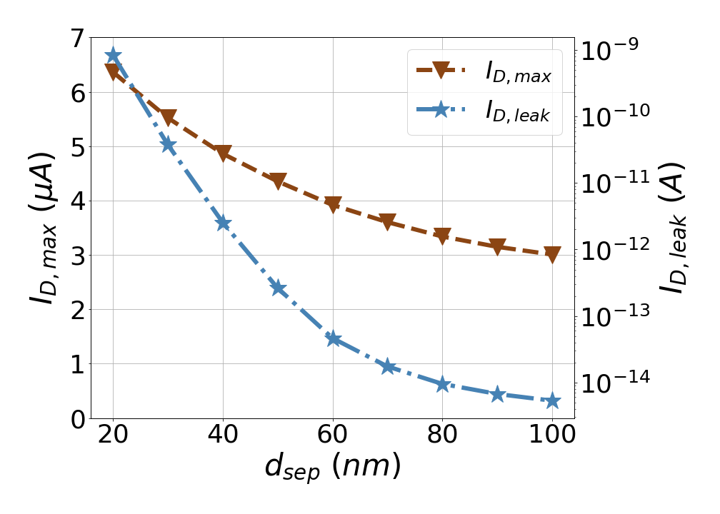
The and v.s. at is shown in Figure 6, where the and reduces significantly with increase in . At , increased to where as increased to compared with the transistor characteristics without MIV. Also, please note the log axis for in the Figure 6. At higher i.e., at , the increases by and increases by compared with the transistor characteristics without MIV. Therefore, has significant impact on the leakage of the transistor and should be considered as a design consideration for MIV placement to ensure proper M3D-IC realizations. Please note that, is the distance between MIV and the transistor and can be considered as the keep-out-zone for MIV.
III-B Scenario 2 – Horizontal placement of MIV
In this scenario, MIV is placed horizontally or in series with the transistor active region where the centers of transistor channel and MIV are aligned as shown in Figure 7. The transistor is separated from the MIV by distance where two cases are possible depending on the terminals and : 1. – source and – drain and, 2. – drain and – source .
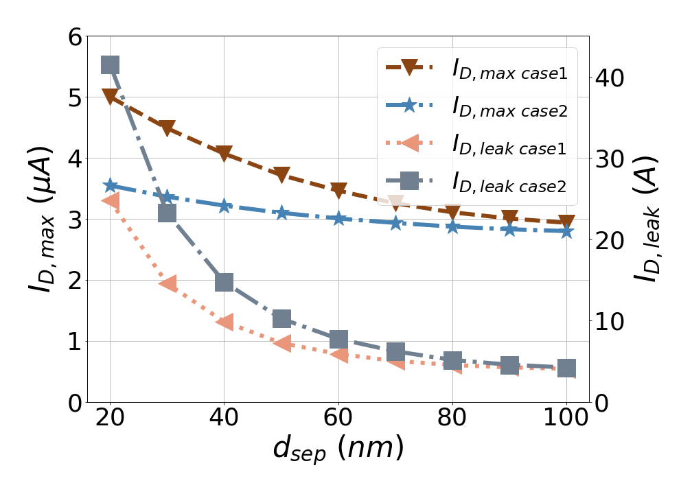
The and v.s. for the two cases i.e., case 1 – as source and case 2 – as drain is shown in Figure 8. The and decreases with increase in . At , the increased by and compared with the transistor without MIV for case 1 and case 2 respectively. increased by and compared with the transistor without MIV at for case 1 and case 2 respectively. At higher i.e., at , the increase only by and 1 for case 1 and case 2 respectively compared with the transistor without MIV. Similarly, increase only by and for case 1 and case 2 respectively compared with the transistor without MIV. Therefore, should be as higher as possible for scenario 2 to ensure not to increase significantly. Although not discussed, the offset distance between MIV and transistor channel reduces both and and should be as high as possible.
Observation 1: Vertical placement of MIV shown in Figure 3 has significant affect on transistor characteristics and require more keep-out distance compared with the horizontal placement of MIV shown in Figure 7.
However, eliminating the vertical placement scenario of MIV is not practically possible in order to obtain higher integration density. Therefore, in the rest of the paper, we consider only the vertical placement scenario of MIV and the same conclusions will also be valid for horizontal placement scenario.
IV Impact of Process Parameters on Transistor Characteristics
One important consideration for M3D-IC design is the process parameters since the sequential integration should be achieved at low temperatures specifically below C [8, 9]. Therefore, the impact of MIV on the transistor characteristics by varying process is an essential study to make practical design considerations since there is no defined process for M3D IC technology. In addition, with the rising demand for heterogeneous integration and mixed-signal IC designs, we believe that it is essential to investigate process parameter affect on transistor characteristics in M3D-IC. For clarity purposes, we consider only Scenario 1 i.e., vertical placement of MIV for this study. First, we systematically study the impact of process parameters on the transistor characteristics in the presence of MIV at in M3D-IC using control variable method to change one parameter at a time. The nominal values of these parameters are given Table I.
IV-A MIV thickness (tmiv)
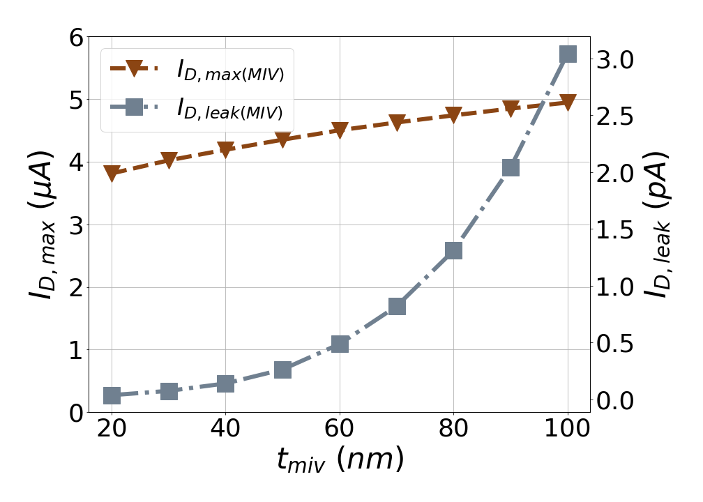
and v.s. is shown in Figure 9. The nominal and obtained for the transistor without MIV is and respectively. Note that the transistor characteristics without MIV does not change with . From the figure, we can see that the increases almost linearly from , when to , when compared with nominal . Also, the increases from , when to , when compared with the nominal . Therefore, the MIV affect is more prominent on the , and this effect should be considered while placing MIV near transistors. From previous observations, we know that will reduce with , and hence the increase in require more (or KOZ) from the transistor to ensure lower .
IV-B MIV liner thickness (tox)
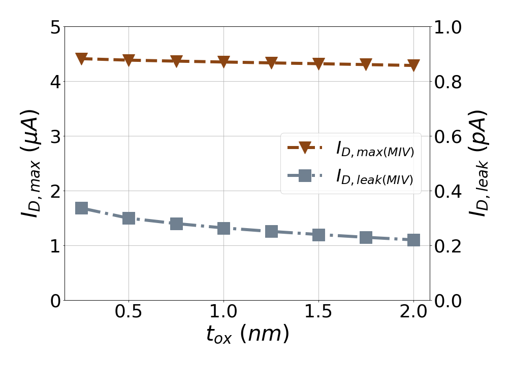
and v.s. is shown in Figure 10. The nominal and obtained for the transistor without MIV is and respectively. Note that the transistor characteristics without MIV does not change with . From the figure, we can see that the almost remains constant at around increase compared with nominal . decreases with increase in where it is , when to , when compared with the nominal . Therefore, higher is desired for reducing MIV impact on leakage current.
IV-C Height of Substrate (Hsub)
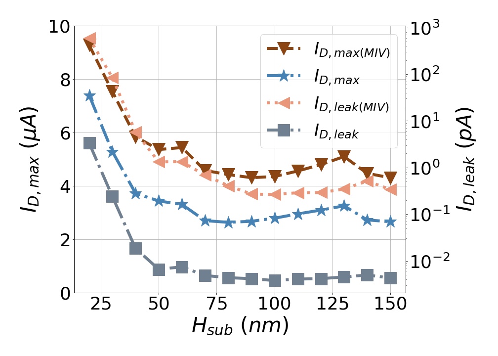
and v.s. obtained for transistor with MIV and without MIV is shown in Figure 11. In this case, the transistor characteristics without MIV will also change with and therefore the and of transistor without MIV is also included in Figure 11, where the plots labeled as and correspond to the transistor without MIV case and the plots labeled as and corresponds to the transistor with MIV case. From the figure, the presence of MIV near the transistor increases both and compared with the transistor without MIV presence. From the figure, we see that increases by up to in MIV presence at nominal separation compared with the case without MIV. Similarly, increases by up to . One important thing to consider is that the height of substrate also affects the minimum thickness of MIV due to the change in aspect ratio of MIV and hence we cannot increase the substrate height significantly.
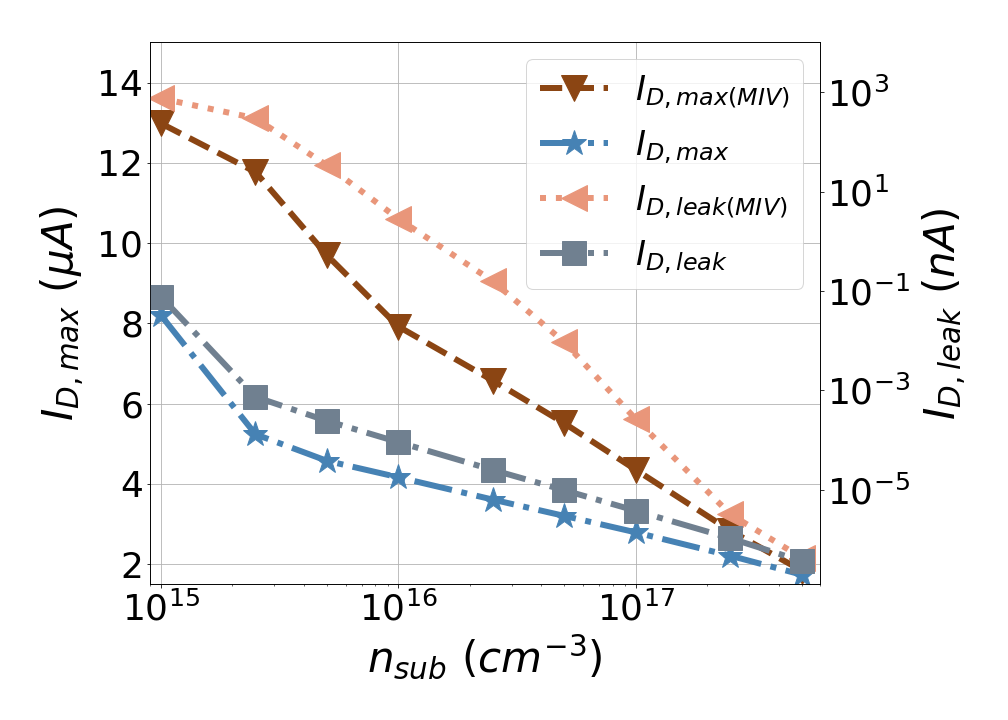
IV-D Substrate Doping (nsub)
and v.s. characteristics for transistor with MIV and without MIV is shown in Figure 12. From the figure, we see that as increases, the decreases for both transistor in presence of MIV and transistor without MIV cases. However, the presence of MIV increases both and of the transistor compared with the transistor without MIV. We also found that and increases by up to and respectively with MIV presence. Also, the nominal is and therefore if the ratio is higher, the leakage will be very high because of higher reverse saturation current at drain and substrate boundary. In addition, we know that the depletion region between the drain and substrate will increase with the decrease of substrate doping [26] and therefore the impact of MIV on is higher at the lower .
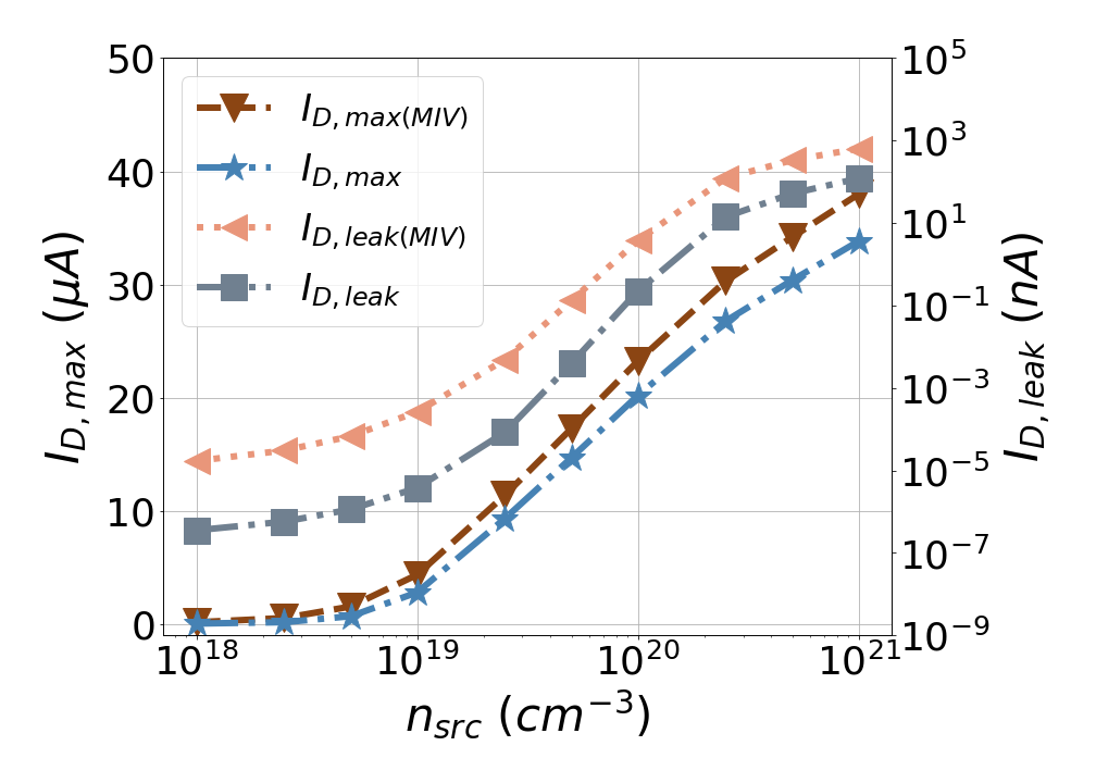
IV-E Active Doping (nsrc)
and v.s. is shown in Figure 13. From the figure, we see that the increases in the linear scale where as the increases exponentially for both transistor with MIV and without MIV cases. As increases up to , presence of MIV resulted in increased leakages ranging from to . We also observed that the increases by up to and increases by up to for transistor with MIV presence compared with the transistor without MIV. We also observed that increases significantly with the increase of and, therefore the ratio should not be very high.
Observation 2: has significant impact on the leakage current of the transistor, when the other process parameters are assumed to be nominal values shown in Table I and MIV is placed at .
—c—c—c—c—c—c—c—c—c—c—c—
V Keep-out-Zone for MIV in M3D-IC process
In this section, we consider three process parameters, specifically substrate height , substrate doping and source/drain doping to study the impact of MIV at the assumed process for realizing the transistor at M3D-IC technology. We assume that to be and and varied the from to . The substrate height is also varied from to . For these cases, we assume the thickness of MIV to be and the liner thickness to be . The impact of MIV placed at away from the transistor of width on the transistor characteristics is shown in Table IV-E. From the table, we can see that at higher (i.e., last three rows colored in blue), the leakage is not significantly increased with MIV presence compared with the transistor leakage without MIV. At lower , the MIV presence has significant impact on the leakage where the increased more than compared with the transistor leakage without MIV (i.e., top rows colored in red) and is increased by up to . Therefore, the M1 metal pitch of () is not sufficient to ensure the reliability of M3D-IC design. From Table V, we can say that keep-out-zone (KOZ or minimum ) between MIV and the transistor is needed to ensure reliability of the M3D-IC realization, and is highly dependent on the , and of the transistor.
—c—c—c—c—c—c—
400 450 500 500
200 200 200 200
200 250 200 200
100 100 100 100
50 100 100 100
50 50 50 50
50 50 50 50
50 50 50 50
Note: KOZ is defined as the minimum spacing around MIV where no other active devices should be formed. is the distance between MIV and the transistor placed near by. Therefore, the minimum required and KOZ are same.
Table V shows the KOZ in nm for the different process parameters of the transistors where we assumed that the KOZ increases in steps of . The KOZ value is obtained when the of the transistor placed near MIV is less than compared to the transistor without MIV. From the table, we can see that transistor process-aware KOZ for MIV is essential for proper operation of the M3D-IC design where the KOZ value can range between to for the assumed variations in the process parameters specifically , and . Therefore, at floorplanning and placement stage of M3D-IC designs, we need to consider these KOZ considerations, and is dependent on the nearby transistor specifications. For example, assume a transistor near MIV has the process parameters as , and then the KOZ for MIV should be at least .
VI Future Directions
In this work, we focused on the thin silicon substrate of 25nm – 100 nm thickness for top-layer in M3D-IC technology. Our future work will also focus on the effect of MIV when multiple transistors are placed around it and the process-aware KOZ of MIV-based design optimization for M3D-IC circuits. However, there are also demonstrations on the FDSOI device with ultra-thin channel in the range of 6nm – 10nm [15, 27, 6, 8, 14, 28]. For this top-layer realization, the back-gate bias for top-layer FDSOI devices should be investigated for coupling reduction from the bottom-layer devices and interconnects. Although the MIV does not pass through the substrate for top-layer FDSOI devices, the device will be adjacent to the MIV depending on the MIV minimum distance. The channel with the MIV will also form the MIS structure but with thick oxide defined by the separation between MIV and adjacent device. Therefore, the MIV impact on the device characteristics should also be considered for reliable top-layer devices since MIV can potentially turn on the channel and increase leakage due to the capacitive coupling. Also, FinFET based top-layer devices are also realized in M3D-IC technology [18]. Similar study for the effect of FinFET device characteristics with MIV adjacent to it should also be considered for the reliable M3D-IC implementations.
Capacitive coupling between MIV and the substrate is considered to realize MIV-devices thus reducing the MIV area overhead in [10, 11]. Similar study considering this MIS structure for ultra-thin FDSOI devices can be considered. In addition, the placement and routing considerations of power delivery networks (PDN) and clock distribution networks (CDN) considering MIVs to route between layers should be studied.
VII Conclusions
In this work, we have discussed the impact of MIV on the surrounding substrate region and on the transistor placed near MIV. We have performed a systematic study on the effect of MIV on the characteristics of the transistor when an MIV is placed near the transistor at different orientations. We then demonstrated that the process parameters specifically substrate doping and source/drain doping of the transistor have a significant effect on the leakage current of the transistor. Finally, we studied the minimum KOZ requirement for the M3D-IC process where we assumed that the substrate doping, source doping and substrate height as parameters and obtained KOZ for each possible process parameter with the assumed M3D-IC process.
Acknowledgements
This work is supported by National Science Foundation under Award number – 2105164.
References
- [1] U. R. Tida, R. Yang et al., “On the Efficacy of Through-Silicon-Via Inductors,” IEEE Transactions on Very Large Scale Integration (VLSI) Systems, vol. 23, no. 7, pp. 1322–1334, 2015.
- [2] U. R. Tida, C. Zhuo, and Y. Shi, “Single-Inductor–Multiple-Tier Regulation: TSV-Inductor-Based On-Chip Buck Converters for 3-D IC Power Delivery,” IEEE Transactions on Very Large Scale Integration (VLSI) Systems, vol. 27, no. 10, pp. 2305–2316, 2019.
- [3] U. R. Tida, C. Zhuo et al., “Dynamic Frequency Scaling Aware Opportunistic Through-Silicon-Via Inductor Utilization in Resonant Clocking,” IEEE Transactions on Computer-Aided Design of Integrated Circuits and Systems, vol. 39, no. 2, pp. 281–293, 2020.
- [4] D. Li, M. S. Vemuri, and U. R. Tida, “An Improved Quadrature Voltage-Controlled Oscillator with Through-Silicon-Via Inductor in Three-dimensional Integrated Circuits,” arXiv preprint arXiv:2001.10678, 2020.
- [5] S. Panth, K. Samadi et al., “High-density integration of functional modules using monolithic 3D-IC technology,” in 18th Asia and South Pacific Design Automation Conference (ASP-DAC), 2013, pp. 681–686.
- [6] C. Fenouillet-Beranger, B. Previtali et al., “FDSOI bottom MOSFETs stability versus top transistor thermal budget featuring 3D monolithic integration,” in 44th European Solid State Device Research Conference (ESSDERC), 2014, pp. 110–113.
- [7] B. Rajendran, R. S. Shenoy et al., “Low Thermal Budget Processing for Sequential 3-D IC Fabrication,” IEEE Transactions on Electron Devices, vol. 54, no. 4, pp. 707–714, 2007.
- [8] M. Vinet, P. Batude et al., “Opportunities brought by sequential 3D CoolCube™ integration,” in 2016 46th European Solid-State Device Research Conference (ESSDERC), 2016, pp. 226–229.
- [9] H. Han, R. Choi et al., “Low Temperature and Ion-Cut Based Monolithic 3D Process Integration Platform Incorporated with CMOS, RRAM and Photo-Sensor Circuits,” in IEEE International Electron Devices Meeting (IEDM), 2020, pp. 15.6.1–15.6.4.
- [10] M. S. Vemuri and U. Rao Tida, “Dual-Purpose Metal Inter-layer Via Utilization in Monolithic Three-Dimensional (M3D) Integration,” in IEEE 63rd International Midwest Symposium on Circuits and Systems (MWSCAS), 2020, pp. 424–427.
- [11] U. R. Tida and M. S. Vemuri, “Efficient Metal Inter-Layer Via Utilization Strategies for Three-dimensional Integrated Circuits,” in IEEE 33rd International System-on-Chip Conference (SOCC), 2020, pp. 195–200.
- [12] B. Rajendran, A. K. Henning et al., “Pulsed laser annealing: A scalable and practical technology for monolithic 3D IC,” in 2013 IEEE International 3D Systems Integration Conference (3DIC), 2013, pp. 1–5.
- [13] A. W. Topol, D. C. L. Tulipe et al., “Three-dimensional integrated circuits,” IBM Journal of Research and Development, vol. 50, no. 4.5, pp. 491–506, 2006.
- [14] P. Batude, C. Fenouillet-Beranger et al., “3DVLSI with CoolCube process: An alternative path to scaling,” in 2015 Symposium on VLSI Technology (VLSI Technology), 2015, pp. T48–T49.
- [15] P. Batude, B. Sklenard et al., “3D sequential integration opportunities and technology optimization,” in IEEE International Interconnect Technology Conference, 2014, pp. 373–376.
- [16] C. Yan and E. Salman, “Mono3D: Open Source Cell Library for Monolithic 3-D Integrated Circuits,” IEEE Transactions on Circuits and Systems I: Regular Papers, vol. 65, no. 3, pp. 1075–1085, 2018.
- [17] P. Shukla, A. K. Coskun et al., “An Overview of Thermal Challenges and Opportunities for Monolithic 3D ICs,” in Proceedings of the 2019 on Great Lakes Symposium on VLSI, ser. GLSVLSI ’19. New York, NY, USA: Association for Computing Machinery, 2019, p. 439–444.
- [18] K. Chang, K. Acharya et al., “Impact and Design Guideline of Monolithic 3-D IC at the 7-nm Technology Node,” IEEE Transactions on Very Large Scale Integration (VLSI) Systems, vol. 25, no. 7, pp. 2118–2129, 2017.
- [19] T. Naito, T. Ishida et al., “World’s first monolithic 3D-FPGA with TFT SRAM over 90nm 9 layer Cu CMOS,” in 2010 Symposium on VLSI Technology, 2010, pp. 219–220.
- [20] D. C. Sekar and Z. Or-Bach, “Monolithic 3D-ICs with single crystal silicon layers,” in 2011 IEEE International 3D Systems Integration Conference (3DIC), 2011 IEEE International, 2012, pp. 1–2.
- [21] K. Dhananjay, P. Shukla et al., “Monolithic 3D Integrated Circuits: Recent Trends and Future Prospects,” IEEE Transactions on Circuits and Systems II: Express Briefs, vol. 68, no. 3, pp. 837–843, 2021.
- [22] J. Shi, D. Nayak et al., “A 14nm FinFET transistor-level 3D partitioning design to enable high-performance and low-cost monolithic 3D IC,” in IEEE International Electron Devices Meeting (IEDM), 2016, pp. 2.5.1–2.5.4.
- [23] S. K. Samal, D. Nayak et al., “Monolithic 3D IC vs. TSV-based 3D IC in 14nm FinFET technology,” in IEEE SOI-3D-Subthreshold Microelectronics Technology Unified Conference (S3S), 2016, pp. 1–2.
- [24] J. De Messemaeker, O. V. Pedreira et al., “Impact of oxide liner properties on TSV Cu pumping and TSV stress,” in IEEE International Reliability Physics Symposium, 2015, pp. 4C.5.1–4C.5.10.
- [25] Y.-H. Gong, J. Kong, and S. W. Chung, “Quantifying the Impact of Monolithic 3D (M3D) Integration on L1 Caches,” IEEE Transactions on Emerging Topics in Computing, vol. 9, no. 2, pp. 854–865, 2021.
- [26] N. Rinaldi, “Analysis of the depletion layer of exponentially graded p-n junctions with nonuniformly doped substrates,” IEEE Transactions on Electron Devices, vol. 47, no. 12, pp. 2340–2346, 2000.
- [27] P. Batude, M. Vinet et al., “Advances, challenges and opportunities in 3D CMOS sequential integration,” in 2011 International Electron Devices Meeting, 2011, pp. 7.3.1–7.3.4.
- [28] P. Batude, L. Brunet et al., “3D Sequential Integration: Application-driven technological achievements and guidelines,” in 2017 IEEE International Electron Devices Meeting (IEDM), 2017, pp. 3.1.1–3.1.4.