One-dimensional electronic structure of phosphorene chains
Abstract
Phosphorene, a 2D allotrope of phosphorus, is technologically very appealing because of its semiconducting properties and narrow band gap. Further reduction of the phosphorene dimensionality may spawn exotic properties of its electronic structure, including lateral quantum confinement and topological edge states. Phosphorene atomic chains self-assembled on Ag(111) have recently been characterized structurally but were found by angle-resolved photoemission (ARPES) to be electronically 2D. We show that these chains, although aligned equiprobably to three \hkl¡1 -1 0¿ directions of the Ag(111) surface, can be characterized by ARPES because the three rotational variants are separated in the angular domain. The dispersion of the phosphorus band measured along and perpendicular to the chains reveals pronounced electronic confinement resulting in a 1D band, flat and dispersionless perpendicular to the chain direction in momentum space. Our density functional theory calculations reproduce the 1D band for the experimentally determined structure of P/Ag(111). We predict a semiconductor-to-metal phase transition upon increasing the density of the chain array so that a 2D structure would be metallic.
I Introduction
Since the first experiments with exfoliated graphene, the field of two-dimensional (2D) quantum materials is in the expansive spotlight of fundamental and applied research. Post-graphene 2D materials are formed not only by group IV elements, but also group V, where the latter demonstrate semiconducting properties: prominent examples are bismuthene [1] and recently synthesized arsenene [2]. One of the most intriguing elements of this type is phosphorus and its allotropes, revealing diversity of novel electronic and optical properties. There are several structural polymorphs such as red, green and blue phosphorus. Black phosphorus (BlackP) is the most stable one, it is a layered material composed of buckled honeycomb sheets of P atoms, held together by van der Waals interaction [3, 4, 5, 6]. The tunability of the band gap in BlackP in wide range (0.32.0 eV), combined with high carrier mobility, makes BlackP a perspective material for electronic design [7] and it has already given promising results in transistor and optoelectronic devices [8, 9]. However, BlackP is difficult to grow epitaxially, therefore, the mechanical/liquid exfoliation techniques used to produce few- and single-layer BlackP limit the bottom-up approach that is needed for integrated circuit development.
Another 2D polymorph with structural and electronic similarities to monolayer BlackP is the blue phosphorene (BlueP). So far formation of BlueP-like structures has been only reported on noble metal substrates [10, 11, 12, 13, 14]. In contrast to the bulk and bulk exfoliated systems, epitaxially grown 2D materials cannot easily be characterized optically, in particular when grown on metals substrates. Hence, the discovery of BlueP proceeded in two steps. At first, the candidate material monolayer P/Au(111) has been investigated structurally by STM [11, 10]. In a second step, angle-resolved photoemission investigated the band dispersion and confirmed the band gap of 1.1 eV of BlueP [15, 16].
A major further step in the design and control of electronic structure of phosphorus would be further reduction of phosphorene dimensionality. Theory predicts that 1D P should host a plethora of interesting phenomena, including giant Stark effect [17] and strain-induced topological phase transition [18]. It is, however, difficult to produce 1D atomic chains and also nanowires from 2D materials since their basis is their weak perpendicular but strong lateral interaction. Nevertheless, nanoribbons have been produced successfully from graphene [19], phosphorene [20] and TMDCs [21].
Recently, it was shown that phosphorus on Ag(111) can self-assemble into 1D atomic chains with an armchair structure [22]. Band structure of an equidistant array of such chains was studied by micro-focused angle-resolved photoemission (ARPES) [22]. It was found to be 2D and not sharp, which led to the conclusion that phosphorus chains are only quasi-1D and exhibit a non-negligible mutual lateral interaction [22]. It should be noted that there are not many cases also for metallic 1D systems where the electronic confinement to 1D on the surface could be proven by ARPES, most notable ones are nanowires of Au on stepped Si(111) [23, 24], In [25, 26] and Pb [27, 28] on Si(111), Tb on Si(110) [29], Au/Ni(110) [30] and a special case of Bi(441) where two 1D surface-localized states were observed [31].
Due to the small size of structural domains even applying micro-focused ARPES at the cost of lower intensity (compared to conventional ARPES) does not guarantee to capture a single local domain of the structure. In the present work we use conventional ARPES and demonstrate that atomic chains of P on Ag(111) exhibit very pronounced and perfectly 1D electronic structure. Phosphorus bands disperse between 3 and 1.5 eV binding energy (EB) in the direction along the chains, but remain extraordinary flat (within 20 meV) in the direction perpendicular to the chains at any EB. This result is accurately confirmed by density functional theory (DFT) calculations. Using DFT we also study the evolution of the phosphorus bands with changing separation between P chains, and find a 1D2D electronic structure transition for marginally separated chains, which renders them a 2D metal.
Information on experimental techniques and DFT calculations is provided in the supporting information [33].
II Results and discussion
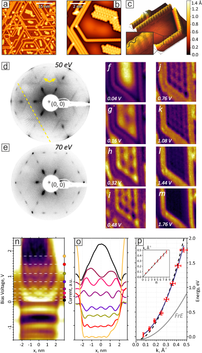
Figs. 1(a,b) display characterization of P chains on Ag(111) by scanning tunneling microscopy (STM) at moderate P coverage (0.6 ML) and at different length scales. P forms mainly 1D structures; however, there are some small 2D islands with lattice rotated by 30∘ relative to the chains. Fig. 1(c) shows a 3D close-up of the chains, which reveals their armchair atomic structure. From STM images one sees that P chains are aligned along three equivalent orientations with a mutual angle of 120∘ between them. These orientations correspond to the \hkl¡1 -1 0¿ family of directions of Ag(111). The formation of three orientational domains of P chains is also confirmed by low-energy electron diffraction (LEED) [Figs. 1(d,e)]. The displayed LEED patterns correspond to a sample with high P coverage, similar to the sample that was used for ARPES measurements. The LEED reveals a (23) pattern which is a superposition of three equally intense (31) superlattices and weak (12) lines (marked by arrows and dashed line), corresponding to the chains in each of the three domains. The complex appearance of the LEED pattern is discussed in the supporting information [33]. In this scenario, the elongation of spots can be explained by an imperfection of chain stacking in the directions perpendicular to the chains. XPS spectra of P 2p and Ag 3d core levels (Fig. S1 of supporting information [33]) are in agreement (within 0.1 eV) with Ref. [22]. According to Ref. [22] the fact that Ag 3d peaks show no chemical shifts as compared to bare Ag implies weak interaction between chains and the substrate and rules out P-Ag surface alloying. We observe only a small shift of Ag 3d core levels to higher EB for chains (80 meV) and larger shift (130 meV) for 2D phase of phosphorus on Ag(111) (Fig. S1). The lack of Ag-P surface alloy is indirectly confirmed in scanning tunneling spectroscopy (STS) experiments, in particular mapping of the Ag(111) surface state (SS) scattering at P chains. A series of quantum interference patterns (QIP) acquired differentially at various binding energies (bias voltages) is displayed in Figs. 1(f–m). The real-space periodicity of standing electron waves, converted to momentum space [Figs. 1(n–p)], allows to determine the E(k) dispersion of Ag(111) SS [34, 32] laterally confined between P chains. A parabolic fitting of the dispersion provides effective mass and apex energy meV. The dispersion was found to be similar to that of the SS at bare Ag(111) [32], except for 50 meV lower binding energy: and meV. This proves that the lateral potential barrier of P chains is so large that the particle-in-a-box model of quantization applies here. This together with our XPS results, which exclude P-Ag surface alloying, demonstrates that there is no leaking of Ag(111) SS into the bulk at the sites of the chains. We conclude that P chains reside on top of Ag(111) and interact with the substrate.
The photoelectrons in ARPES are collected from the whole area illuminated by the photon beam. Even with the use of micro-focused ARPES, discerning a signal from a single domain might be very challenging because of the small average size of uniaxially aligned domains. In the present experiment beam size is on the scale of 100 m. This means that signals from all three orientational domains of P chains are accumulated and superimposed in the ARPES dispersions. For ARPES investigation of 1D structures it is optimal to have them identical and aligned along a single direction in order to be able to clearly separate electronic bands dispersing along the chain and non-dispersing bands of electrons confined in the perpendicular direction.
However, we show below that in the current case conventional ARPES is well applicable for mapping of the 1D electronic structure because the maxima of P valence bands are far away from the center of the surface Brillouin zone (SBZ). As a result, 1D bands of chains with different orientations only partially overlap in k-space.
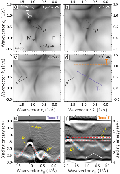
Figs. 2(a–d) report a series of constant energy surfaces (CES) of P chains on Ag(111) extracted from full photoemission mapping I(E,kx,ky) for different binding energies. Circular-like contours labeled as Ag-sp correspond to nearly spherical 3D bulk sp-bands of Ag and surface resonances related to them [35]. Electronic states of P chains are seen between Ag-sp contours around the point of the Ag(111) SBZ () and are labeled as P. They evolve from a cloverleaf-like pattern at =2.26 eV, through crossing straight double lines at =1.76 eV, and to the triangle of single straight lines at =1.46 eV. These lines belong to the 1D band structure of P chains. Every side of the triangle is emitted from one of the chain orientations, as sketched in Fig. 3(a). The overall ARPES dispersion of the band P along the direction of Ag(111) SBZ [trace T1 in Fig. 2(d)], which corresponds to the direction along the chains of one of the domains, is depicted in Fig. 2(e) and emphasized by a dashed red line. It has several valleys and shows a pronounced dispersion in a wide energy range between =3 eV and 1.5 eV. A second band P’ (marked by a dashed blue line) is a contribution from two other rotated domains sliced at an angle to a high symmetry direction (therefore, it appears stretched along the k∥ axis, as compared to P).
The dispersion in Fig. 2(e) reveals the top of chain band P at 1.5 eV. This shows that the intrinsic band gap of phosphorene chains is not less than 1.5 eV, in agreement with our DFT calculations in Fig. 4.
The 1D character of the P band becomes evident when one measures its dispersion in the direction perpendicular to the P chains. The ARPES slice along the straight line seen in the CES [trace T2 in Fig. 2(d)] is shown in Fig. 2(f). It reveals perfectly flat slices of the P band, dispersionless within 20 meV. Signals from other rotational domains (P’) are also seen there. The band seen at 3.5 eV (white arrows) can be attributed to lower lying P band, which is also predicted by our DFT calculations [see Fig. 4(d)].
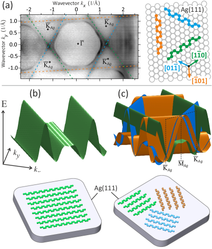
A sketch of the 1D band of P chains is shown in Fig. 3(b). The model of band superposition for three orientational domains is displayed in Fig. 3(c). This model explains ARPES observations near the point of the Ag(111) SBZ, including the cloverleaf-like pattern at higher EB and triangular crossings of double and single straight lines at lower . The cross-section on the left side of Fig. 3(c) closely resembles Fig. 2(f). Additional APRES characterization of this superpositional band structure is reported in the supporting information [33].
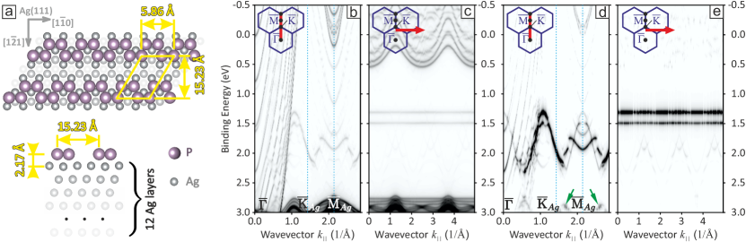
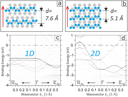
We also performed a density functional theory (DFT) study of the P chains on Ag(111). It was assumed that chains are parallel to each other and form a periodic array. This phase corresponds to the high-phosphorus-coverage sample used for ARPES measurements and reflects the structure of a single rotational domain [22]. For the model which reproduces the experimentally synthesized chains resolved by our LEED and STM [(23) relative to Ag(111), Fig. 4(a)], the electronic structure of P chains was confirmed as purely 1D. The overall band structure comprising P and Ag states along the direction [ to chains] and [ to chains] is shown in Figs. 4(b,c). A projection on P atoms is presented in Figs. 4(d,e). Good qualitative agreement with the ARPES experiment is seen, including the dispersionless character of the P chain band perpendicular to the chains direction due to confinement.
Furthermore, by DFT we studied how the band structure of the P chains within the array depends on the lateral separation d between them. While the experimentally realized Å [Ag(111)/P-(23)] hosts a 1D P band, a denser simulated array with Å [Ag(111)/P-] triggers inter-chain interaction and causes a 1D2D transition in the electronic structure of the array. The dispersions of the P state calculated for the experimentally synthesized ( Å) and for artificial ( Å) arrays are compared vis-à-vis in Figs. 5(c) and 5(d), respectively. One sees that in the denser array the P band is not flat but disperses strongly and even crosses the Fermi level (), hence rendering the chains metallic.
Finally, we tested the presence of topological edge states, predicted for the armchair configuration [36]. These states should appear as nearly flat bands in the vicinity of . We found no such bands below in ARPES and no visible signs of them in STS. The absence of topological states can be attributed to their suppression by confinement. According to Ref. [36], the localization of edge states requires a phosphorene nanoribbon with minimal width of 56 lattice constants, which is not realized in P chains.
III Conclusion
In summary, we studied phosphorene atomic chains self-assembled on a Ag(111) substrate in the armchair configuration. Although the chains grow in three equiprobable orientations, aligned to the \hkl¡1 -1 0¿ family of directions of Ag(111) rotated by 120∘ to each other, we show that conventional ARPES can be used for the mapping of their band structure because their bands are separated in the angular domain. We have measured the dispersion of the chain band and show that it is 1D: The band disperses within 1.5 eV along the chain but remains perfectly flat and dispersionless in the direction perpendicular to the chain due to lateral confinement. Our DFT calculations confirm this result and predict a 1D2D transition in the electronic structure of the chain array when the lateral separation between the chains is reduced. This transition also changes the band structure of the chains from semiconducting (with intrinsic band gap eV) to metallic.
IV Acknowledgments
This work was supported by Impuls- und Vernetzungsfonds der Helmholtz-Gemeinschaft under grant no. HRSF-0067.
V Conflict of interest
The authors declare no conflict of interest.
References
- Reis et al. [2017] F. Reis, G. Li, L. Dudy, M. Bauernfeind, S. Glass, W. Hanke, R. Thomale, J. Schäfer, and R. Claessen, Bismuthene on a SiC substrate: A candidate for a high-temperature quantum spin Hall material, Science 357, 287 (2017).
- Shah et al. [2020] J. Shah, W. Wang, H. M. Sohail, and R. I. G. Uhrberg, Experimental evidence of monolayer arsenene: an exotic 2D semiconducting material, 2D Mater. 7, 025013 (2020).
- Ling et al. [2015] X. Ling, H. Wang, S. Huang, F. Xia, and M. S. Dresselhaus, The renaissance of black phosphorus, PNAS 112, 4523 (2015).
- Han et al. [2014] C. Q. Han, M. Y. Yao, X. X. Bai, L. Miao, F. Zhu, D. D. Guan, S. Wang, C. L. Gao, C. Liu, D. Qian, Y. Liu, and J.-f. Jia, Electronic structure of black phosphorus studied by angle-resolved photoemission spectroscopy, Phys. Rev. B 90, 085101 (2014).
- Xia et al. [2019] F. Xia, H. Wang, J. C. M. Hwang, A. H. C. Neto, and L. Yang, Black phosphorus and its isoelectronic materials, Nat. Rev. Physics 1, 306 (2019).
- Golias et al. [2016] E. Golias, M. Krivenkov, and J. Sánchez-Barriga, Disentangling bulk from surface contributions in the electronic structure of black phosphorus, Phys. Rev. B 93, 075207 (2016).
- Kim et al. [2015] J. Kim, S. S. Baik, S. H. Ryu, Y. Sohn, S. Park, B.-G. Park, J. Denlinger, Y. Yi, H. J. Choi, and K. S. Kim, Observation of tunable band gap and anisotropic Dirac semimetal state in black phosphorus, Science 349, 723 (2015).
- Li et al. [2014] L. Li, Y. Yu, G. J. Ye, Q. Ge, X. Ou, H. Wu, D. Feng, X. H. Chen, and Y. Zhang, Black phosphorus field-effect transistors, Nat. Nanotechnol. 9, 372 (2014).
- Xia et al. [2014] F. Xia, H. Wang, and Y. Jia, Rediscovering black phosphorus as an anisotropic layered material for optoelectronics and electronics, Nat. Commun. 5, 4458 (2014).
- Zhang et al. [2016] J. L. Zhang, S. Zhao, C. Han, Z. Wang, S. Zhong, S. Sun, R. Guo, X. Zhou, C. D. Gu, K. D. Yuan, Z. Li, and W. Chen, Epitaxial growth of single layer blue phosphorus: A new phase of two-dimensional phosphorus, Nano Lett. 16, 4903 (2016).
- Zhang et al. [2018] W. Zhang, H. Enriquez, Y. Tong, A. Bendounan, A. Kara, A. P. Seitsonen, A. J. Mayne, G. Dujardin, and H. Oughaddou, Epitaxial synthesis of blue phosphorene, Small 14, 1804066 (2018).
- Schaal et al. [2021] M. Schaal, J. Picker, F. Otto, M. Gruenewald, R. Forker, and T. Fritz, An alternative route towards the fabrication of 2D blue phosphorene, J. Phys.: Condens. Matter 33, 485002 (2021).
- Yang et al. [2020] S. Yang, Z. Hu, W. Wang, P. Cheng, L. Chen, and K. Wu, Regular arrangement of two-dimensional clusters of Blue Phosphorene on Ag(111), Chin. Phys. Lett. 37, 096803 (2020).
- Zhang et al. [2022] J. Zhang, X. Dong, S. Xu, Y. Xia, W. Ho, H. Xu, and M. Xie, Metal-phosphorus network on Pt(111), 2D Mater. 9, 045002 (2022).
- Zhuang et al. [2018] J. Zhuang, C. Liu, Q. Gao, Y. Liu, H. Feng, X. Xu, J. Wang, J. Zhao, S. X. Dou, Z. Hu, and Y. Du, Band gap modulated by electronic superlattice in blue phosphorene, ACS Nano 12, 5059 (2018).
- Golias et al. [2018] E. Golias, M. Krivenkov, A. Varykhalov, J. Sánchez-Barriga, and O. Rader, Band renormalization of blue phosphorus on Au(111), Nano Lett. 18, 6672 (2018).
- Wu et al. [2015] Q. Wu, L. Shen, M. Yang, Y. Cai, Z. Huang, and Y. P. Feng, Electronic and transport properties of phosphorene nanoribbons, Phys. Rev. B 92, 035436 (2015).
- Taghizadeh Sisakht et al. [2016] E. Taghizadeh Sisakht, F. Fazileh, M. H. Zare, M. Zarenia, and F. M. Peeters, Strain-induced topological phase transition in phosphorene and in phosphorene nanoribbons, Phys. Rev. B 94, 085417 (2016).
- Cai et al. [2010] J. Cai, P. Ruffieux, R. Jaafar, M. Bieri, T. Braun, S. Blankenburg, M. Muoth, A. P. Seitsonen, M. Saleh, X. Feng, K. Müllen, and R. Fasel, Atomically precise bottom-up fabrication of graphene nanoribbons, Nature 466, 470 (2010).
- Watts et al. [2019] M. C. Watts, L. Picco, F. S. Russell-Pavier, P. L. Cullen, T. S. Miller, S. P. Bartuś, O. D. Payton, N. T. Skipper, V. Tileli, and C. A. Howard, Production of phosphorene nanoribbons, Nature 568, 216 (2019).
- Lim et al. [2022] H. E. Lim, Z. Liu, J. Kim, J. Pu, H. Shimizu, T. Endo, Y. Nakanishi, T. Takenobu, and Y. Miyata, Nanowire-to-nanoribbon conversion in transition-metal chalcogenides: Implications for one-dimensional electronics and optoelectronics, ACS Appl. Nano Mater. 5, 1775 (2022).
- Zhang et al. [2021] W. Zhang, H. Enriquez, Y. Tong, A. J. Mayne, A. Bendounan, A. Smogunov, Y. J. Dappe, A. Kara, G. Dujardin, and H. Oughaddou, Flat epitaxial quasi-1D phosphorene chains, Nat. Commun. 12, 5160 (2021).
- Segovia et al. [1999] P. Segovia, D. Purdie, M. Hengsberger, and Y. Baer, Observation of spin and charge collective modes in one-dimensional metallic chains, Nature 402, 504 (1999).
- Crain et al. [2003] J. N. Crain, A. Kirakosian, K. N. Altmann, C. Bromberger, S. C. Erwin, J. L. McChesney, J.-L. Lin, and F. J. Himpsel, Fractional band filling in an atomic chain structure, Phys. Rev. Lett. 90, 176805 (2003).
- Yeom et al. [1999] H. W. Yeom, S. Takeda, E. Rotenberg, I. Matsuda, K. Horikoshi, J. Schaefer, C. M. Lee, S. D. Kevan, T. Ohta, T. Nagao, and S. Hasegawa, Instability and charge density wave of metallic quantum chains on a silicon surface, Phys. Rev. Lett. 82, 4898 (1999).
- Ahn et al. [2004] J. R. Ahn, J. H. Byun, H. Koh, E. Rotenberg, S. D. Kevan, and H. W. Yeom, Mechanism of gap opening in a triple-band Peierls system: In atomic wires on Si, Phys. Rev. Lett. 93, 106401 (2004).
- Tegenkamp et al. [2008] C. Tegenkamp, T. Ohta, J. L. McChesney, H. Dil, E. Rotenberg, H. Pfnür, and K. Horn, Coupled Pb chains on Si(557): Origin of one-dimensional conductance, Phys. Rev. Lett. 100, 076802 (2008).
- Kim et al. [2007] K. S. Kim, H. Morikawa, W. H. Choi, and H. W. Yeom, Strong lateral electron coupling of Pb nanowires on stepped Si(111): Angle-resolved photoemission studies, Phys. Rev. Lett. 99, 196804 (2007).
- Appelfeller et al. [2023] S. Appelfeller, M. Franz, M. Karadag, M. Kubicki, R. Zielinski, M. Krivenkov, A. Varykhalov, A. Preobrajenski, and M. Dähne, Self-organized formation of unidirectional and quasi-one-dimensional metallic Tb silicide nanowires on Si(110), Appl. Surf. Sci. 607, 154875 (2023).
- Pampuch et al. [2000] C. Pampuch, O. Rader, T. Kachel, W. Gudat, C. Carbone, R. Kläsges, G. Bihlmayer, S. Blügel, and W. Eberhardt, One-dimensional spin-polarized quantum-wire states in Au on Ni(110), Phys. Rev. Lett. 85, 2561 (2000).
- Bianchi et al. [2015] M. Bianchi, F. Song, S. Cooil, A. F. Monsen, E. Wahlström, J. A. Miwa, E. D. L. Rienks, D. A. Evans, A. Strozecka, J. I. Pascual, M. Leandersson, T. Balasubramanian, P. Hofmann, and J. W. Wells, One-dimensional spin texture of Bi(441): Quantum spin hall properties without a topological insulator, Phys. Rev. B 91, 165307 (2015).
- Grothe et al. [2013] S. Grothe, S. Johnston, S. Chi, P. Dosanjh, S. A. Burke, and Y. Pennec, Quantifying many-body effects by high-resolution Fourier transform scanning tunneling spectroscopy, Phys. Rev. Lett. 111, 246804 (2013).
- [33] Supplementary information is available online.
- Hövel et al. [2001] H. Hövel, B. Grimm, and B. Reihl, Modification of the Shockley-type surface state on Ag(111) by an adsorbed xenon layer, Surf. Sci. 477, 43 (2001).
- Krivenkov et al. [2022] M. Krivenkov, D. Marchenko, M. Sajedi, A. Fedorov, O. J. Clark, J. Sánchez-Barriga, E. D. L. Rienks, O. Rader, and A. Varykhalov, On the problem of dirac cones in fullerenes on gold, Nanoscale 14, 9124 (2022).
- Tani et al. [2022] T. Tani, M. Hitomi, T. Kawakami, and M. Koshino, Topological edge and corner states and fractional corner charges in blue phosphorene, Phys. Rev. B 105, 075407 (2022).