Assessing the potential of perfect screw dislocations in SiC for solid-state quantum technologies
Abstract
Although point defects in solids are one of the most promising physical systems to build functioning qubits, it remains challenging to position them in a deterministic array and to integrate them into large networks. By means of advanced ab initio calculations we show that undissociated screw dislocations in cubic 3C-SiC, and their associated strain fields, could be used to create a deterministic pattern of relevant point defects. Specifically, we present a detailed analysis of the formation energies and electronic structure of the divacancy in 3C-SiC when located in the vicinity of this type of dislocations. Our results show that the divacancy is strongly attracted towards specific and equivalent sites inside the core of the screw dislocations, and would form a one-dimensional arrays along them. Furthermore, we show that the same strain that attracts the divacancy allows the modulation of the position of its electronic states and of its charge transition levels. In the case of the neutral divacancy, we find that these modulations result in the loss of its potential as a qubit. However, these same modulations could transform defects with no potential as qubits when located in bulk, into promising defects when located inside the core of the screw dislocations. Since dislocations are still mostly perceived as harmful defects, our findings represent a technological leap as they show that dislocations can be used as active building blocks in future defect-based quantum computers.
A quantum computer is a device that exploits quantum behavior to deal with computational problems that cannot be solved, or would take too long, in a classical computer Nielsen and Chuang (2010); Ladd et al. (2010). In order to build a functioning quantum computer, several physical systems have been proposed as platforms for quantum bits (qubits), e.g., photons Flamini et al. (2018); Slussarenko and Pryde (2019), trapped atoms/ions Häffner et al. (2008); Bruzewicz et al. (2019) and point defects in solids Gruber et al. (1997); Balasubramanian et al. (2009); Doherty et al. (2013); Zhang et al. (2020); Chatterjee et al. (2021); Wolfowicz et al. (2021). The latter system is advantageous from the point of view of scalability since integrated quantum devices could, in principle, be built by means of adapted fabrication techniques developed in the semiconductor industry Koehl et al. (2015). Nevertheless, it remains challenging to position the point defects in a deterministic array and to integrate them into large networks Atatüre et al. (2018).
Currently, the desired array of point defects are created using mainly irradiation and implantation. However, these methods are limited by the beam size on target (positioning accuracy of 30 nm, when achieving a high creation yield) Schröder et al. (2017); Wang et al. (2017); Zhou et al. (2018); Chen et al. (2019); Smith et al. (2019); Castelletto and Boretti (2020). As has been pointed out for the case of two-dimensional materials, alternative to more traditional methods, an engineered strain field is also able to create an array of point defects used as quantum emitters Kumar et al. (2015); Branny et al. (2017). Nevertheless, in that case the regularity of the resulting array is hampered by the precision of the method used to grow the nanopillars that induce the strain field (positioning accuracy of 12032 nm).
Besides the localization and interconnection problems, one further limitation of current defect-based quantum technologies is that usually only point defects are considered as active elements. As a matter of fact, in their seminal work on the potential of point defects for quantum computing, Weber et al. proposed that one of the properties of a suitable host material would be its availability as high-quality single crystals Weber et al. (2010). Up to now, the presence and effects of extended defects (e.g., dislocations, stacking faults, grain boundaries and surfaces) has been considered mostly from the point of view of irregularities to avoid and control Wolfowicz et al. (2021); Stamp and Gaita-Ariño (2009); Bassett et al. (2019); Kaviani et al. (2014); Chou and Gali (2017); Chou et al. (2017); Stacey et al. (2019); Sangtawesin et al. (2019); Li et al. (2019); Shen et al. (2020); Körner et al. (2021, 2022); Löfgren et al. (2022); Dwyer et al. (2022). It was only recently that there has been interest on understanding the possible advantages and applications of extended defects, specifically stacking faults Ivády et al. (2019).
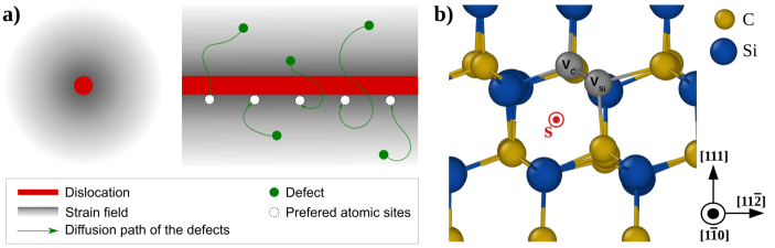
Compared to stacking faults, dislocations have a stronger and longer-range interaction with point defects due to their characteristic strain fields Holt and Yacobi (2007); Hull and Bacon (2011); Cai et al. (2016); Anderson et al. (2017). This means that, as illustrated in Fig. 1(a), qubits built using point defects could be created near an engineered dislocation and, due to the attraction between the qubits and the dislocation, an annealing process would result in a self-assembled one-dimensional array of qubits along the dislocation. Recently, it was shown that certain positions inside the cores of partial dislocations in diamond are preferred locations for NV- centers to form, while conserving the interesting quantum properties of the centers Ghassemizadeh et al. (2022). However, partial dislocations are not radially symmetric, and several undesired configurations of the NV- centers near partial dislocations in diamond are likely to exist Ghassemizadeh et al. (2022). One possible way to overcome these limitations and to effectively harness the potential of dislocations for quantum technologies would be to engineer perfect (undissociated) dislocations, specifically screw dislocations, which have a radially symmetric strain fields and core structures Holt and Yacobi (2007); Hull and Bacon (2011); Cai et al. (2016); Anderson et al. (2017). Another advantage of using this type of dislocations is the fact that it is possible to create ordered and regular two-dimensional arrays of perfect screw dislocations using wafer bonding techniques Reiche et al. (2010, 2014), which would imply the possibility of creating self-assembled two-dimensional arrays of qubits along the screw dislocations.
For this idea to work, we need host materials which satisfy two conditions: screw dislocations prefer to be undissociated and, in that preferred configuration, they are electrically inactive. The latter condition ensures that the relevant quantum properties of the defect-based qubits located along the dislocation are not altered beyond the effect of the strain field associated with the screw dislocation. Among the most relevant host materials for defect-based quantum technologies, silicon carbide is the one exhibiting perfect screw dislocations as stable configurations under normal conditions Pizzagalli et al. (2005); Demenet et al. (2013); Pizzagalli (2014).
In this Letter, we use ab initio simulations to study the strength and effects of the interaction between a perfect screw dislocation in 3C-SiC and the divacancy (DV) in the same material. The DV in 3C-SiC is known to exhibit promising properties as a qubit when in its charge neutral (DV0) configuration Zhang et al. (2020); Castelletto and Boretti (2020); Christle et al. (2017); Son et al. (2020). To carry out our study, we analyze the change in the formation energy and electronic structure of the DV0 when located near the core of the screw dislocation. Our calculations reveal that DV0 prefers to form inside the core at specific and equivalent sites, implying that a one-dimensional array of qubits along the dislocation would be created. In addition, our results show that the same strain that drives the DV0 towards the dislocation core allows the modulation of the position of its electronic states and of its thermodynamic charge transition levels (CTLs).
Perfect screw dislocations in 3C-SiC are located in the shuffle set of the 111 planes with both, its dislocation line and Burgers vector lying in the 110 directions Pizzagalli et al. (2005); Demenet et al. (2013); Pizzagalli (2014). To study such dislocations in their stoichiometric and DV decorated configurations, the structural model used in our simulations contains a dislocation dipole in a quadrupolar arrangement, which minimizes the interaction between dislocations Bulatov and Cai (2006); Rodney et al. (2017); Clouet (2020). Such model is created in a 576-atom SiC supercell using the software package Clouet . This configuration can be seen in the supplementary material, Fig. 4, and guarantees a minimum distance between dislocation cores of 16Å. Our density functional theory (DFT) calculations are performed using the Kresse and Furthmüller (1996) simulation package with a converged plane-wave energy cutoff of 500 eV. The used supercells are built with the experimental lattice parameter of 4.36Å Li and Bradt (1986) and ions are relaxed using the Perdew-Burke-Enzerhof (PBE) Perdew et al. (1996) semi-local functional until forces are below 0.02 eV/Å. To obtain accurate formation energies, charge transition levels and electronic properties, we use the Heyd, Scuseria and Enzerhof (HSE06) Heyd et al. (2003, 2006) hybrid functional on the PBE relaxed supercells. In all cases we use a converged k-point grid. To obtain a reference for our simulations, we performed calculations for the isolated DV in an analogous supercell and using the same computational setup.
Using the described methodology we tackle the first question at hand: does the DV prefer to form in the vicinity of perfect screw dislocation in 3c-SiC? To answer it, we compare the formation energy in a given charge state of an isolated DV, , and that of the same defect when located near the core of the studied dislocation, , which are defined as Freysoldt et al. (2014); Komsa et al. (2012)
| (1) |
and
| (2) |
where is the total energy of the supercell containing an isolated DV in charge state , and is the total energy of the supercell containing the dislocation dipole with one DV, in charge state , near one of the cores. The second term on the right side of both Eqs. 1 and 2 is the total energy of the corresponding reference supercell. In the case of the isolated DV, is the total energy of the pristine supercell. For the case of the DV decorated core, is the total energy of the supercell containing the stoichiometric dislocation dipole. The last three terms on the right in Eqs. 1 and 2 are analogous in both cases. Specifically, in the third term is an integer that indicates the number of atoms of type removed to create the DV and is the chemical potential of the same removed atoms. The fourth term, , accounts for the energy needed to charge the system. It contains the valence band maximum (VBM) energy, , and the Fermi energy, , referenced to the VBM (i.e., their sum tell us where, inside the band gap, is the chemical potential of the electrons). The last term, , accounts for the correction needed to eliminate the spurious electrostatic interactions between periodic images of the defects under study. This correction is calculated using the approach proposed by Freysoldt, Neugebauer and Van de Walle Freysoldt et al. (2009). Note that this approach is only applicable if the dislocations under study are electrically inactive and all the charge added to the supercells is localized at the DVs. To prove the reliability of our methodology, in the supplementary material (Fig. 5) it is possible to see the localized nature of the charge density difference between a DV0 and a charged DV when located directly at the core of the dislocation. The charge density difference was obtained using VESTA Momma and Izumi (2011).
Once and are defined, we can give a quantitative estimation of the strength of the interaction between the screw dislocation and the DV by calculating
| (3) |
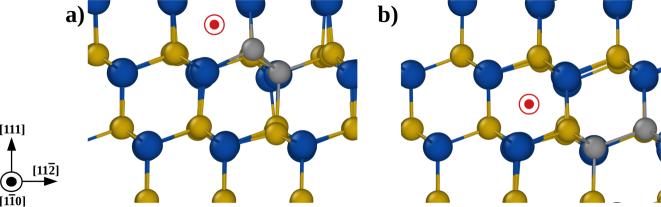
which is negative if the DV prefers to be located near/inside the dislocation core. In the case of the neutral DV0, we found that there is a clear and strong attraction towards the dislocation. Specifically, the DV0 exhibits a eV for all configurations that have both vacancies occupying sites directly at the core of the dislocation. An example of such arrangement is shown on Fig. 1(b). Our calculations show that any other configuration, with the DV0 located further away from the core, implies steep changes in the corresponding and a weaker interaction between the DV0 and the dislocation, i.e., a less negative . For example, the second-preferred configuration has the silicon vacancy directly at the core and the carbon vacancy siting outside the core, and exhibits a eV. The third-preferred configuration, when both vacancies composing the DV0 are located directly outside the core and in the second ring from the center, has a eV. The difference of +0.5 eV between the of the preferred and of the second-preferred, and of +1.6 eV between the of the preferred and of the third-preferred configurations exemplify the strong thermodynamic driving force that pushes the DV0 towards a specific configuration along the dislocations, with both vacancies occupying sites directly at the core. Structural examples of the second- and third-preferred configurations can be seen in Fig. 6 of the supplementary material.
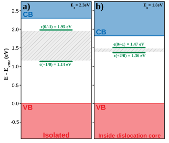
Although this analysis proves that the neutral DV0 is strongly attracted towards specific configurations directly at the core, a complete answer to the aforementioned question can only be given if other stable charge states are also addressed. For this purpose, we compare the CTLs of the isolated DV and those of the same defect when located near the dislocation. Besides allowing us to understand the electrical properties of defects (ionization energies), we decided to use the CTLs due to the fact that their position in the band gap provide us the stability range of the possible charge states. For a given defect, the CTLs are referred to as and are defined as the Fermi energy values at which its formation energy for charge states and become equal Freysoldt et al. (2014); Komsa et al. (2012). Our results for the are shown in Fig. 2. On the one hand, in the case of the isolated DV, we find two CTLs, eV and eV. This means that in 3C-SiC, the DV0 is stable in a large Fermi energy region of eV for n-type doping conditions (around % of the calculated eV band gap for bulk), which is in line with the corresponding results available in literature Gordon et al. (2015); Schultz et al. (2021). On the other hand, when the DV is located at its preferred configurations directly at the core of the screw dislocation, the stability region for the neutral DV0 is drastically reduced. In this case we found two CTLs, eV and eV, that imply a stability region of only eV, which corresponds to % of the 1.8 eV band gap obtained for a dislocated sample (the reduced band gap observed for the supercell containing the dislocation dipole is caused by the band tail states associated to the disorder induced by the dislocations Lee et al. (2000); Barragan-Yani and Albe (2017)). The fact that the stability region of the DV0 is reduced despite its strong interaction with the screw dislocation with eV, means that the interaction between the strain induced by the dislocation and the DV in all its charge states is of the same order of magnitude but larger for higher charges, which is common to other materials and defects Aschauer and Spaldin (2016); Simsek Sanli et al. (2017). Our calculations predict that the configuration preferred by the DV0, with both vacancies sitting directly at the core of the screw dislocation, is also the preferred one for its other stable charge states. Specifically, we obtained eV and eV. These findings imply that screw dislocations in 3C-SiC are able to attract defect-based qubits and induce the formation of one-dimensional qubit arrays, but for the specific case of the DV0 the stability range of the neutral state is drastically reduced. Nevertheless, the possibility of defects with higher charge states reacting more strongly to the strain induced by the dislocation, implies that new defect-based qubits, perhaps unstable in bulk, could be stabilized near screw dislocations in 3C-SiC.
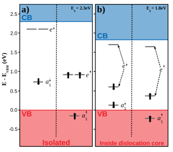
At this point in our assessment we need to answer a second question: are the electronic properties that make a given defect useful as a qubit, unaltered when located in the core of the screw dislocation? Our analysis proved that, due to a reduced stability region, the DV0 would have a limited applicability when located inside the core of the screw dislocation. Nevertheless, we can study its Kohn-Sham states to reveal the effect of the strain field induced by the dislocation on the electronic structure of a potential qubit. In line with available literature on the matter Gordon et al. (2015); Csóré et al. (2022); Gao et al. (2022), our calculations show that the isolated DV0 introduces an occupied state, a doubly occupied and degenerate state, and an unoccupied and degenerate state within the band gap of bulk 3C-SiC (see Fig. 3(a)). In addition, we also find an occupied state just below the valence band maximum. Altogether, the induced states imply a spin triplet ground state for the isolated DV, and its electronic structure satisfies the criteria required for defect-based qubits Weber et al. (2010). As can be seen in Fig. 3(b), in the case of the DV0 located in its preferred configuration inside the screw dislocation core, the degeneracy of the states is lifted. The cause of this change is the localized disorder near the cores, which can be understood using a coordination analysis for the region near the core (see Fig. 7 of the supplementary material). This same disorder is the cause of the band tail states that reduce the band gap in the dislocated supercell Lee et al. (2000); Barragan-Yani and Albe (2017)). The consequence of the degeneracy being lifted is that, compared to the isolated DV0, the DV0 near the core does not introduce a doubly occupied state, but a singly occupied state and a singly occupied state. Together with the occupied , which are common to both the isolated and inside-the-core DV0, the electronic structure shown in Fig. 3(b) implies a spin singlet. This means that, besides seeing its stability region reduced, the DV0 located inside the core of the screw dislocation is not useful as a qubit. However, as it can also be seen in Fig. 3(b), the screw dislocation does not induce any deep state by itself and it allows a defect sitting in its core to have bound states. These findings imply that new defect-based qubits, perhaps useless in bulk, could become paramagnetic by having their electronic degeneracy being lifted near screw dislocations in 3C-SiC.
In conclusion, we propose that, in order to have potential for quantum applications, dislocations should be undissociated screws and be electrically inactive. Such conditions are satisfied in 3C-SiC, and our calculations show that the undissociated screw dislocation in this material is able to attract defect-based qubits into its core. As a consequence, it would allow the creation of a one-dimension array of qubits along its line direction. Furthermore, we show that the strain field induced by this specific dislocation type is able to modulate both, the charge transition levels and the electronic structure of the qubit located in its core, without itself being electrically active. For the specific case of the DV0, our results show that these modulations result in the loss of its potential as a qubit. However, these same modulations could transform defects with no potential as qubits when located in bulk, into promising options when located inside the core of the screw dislocations. Altogether our findings represent a paradigm shift within quantum technologies, as they point out that dislocations can be used as active building blocks of future defect-based quantum computers.
We acknowledge that this project has received funding from the European Union’s Horizon 2020 research and innovation programme under the Marie Skłodowska-Curie grant agreement No 898860. Furthermore, the authors gratefully acknowledge the computing time granted by the HPC facilities of the University of Luxembourg and the HRZ (Lichtenberg-Cluster) at TU Darmstadt.
I Supplementary material
I.1 Supercell configuration
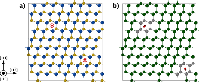
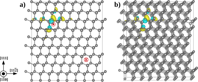
To study perfect stoichiometric and decorated screw dislocations in 3C-SiC, we used supercells containing a dislocation dipole in a quadrupolar arrangement, which minimizes the interaction between dislocations Bulatov and Cai (2006); Rodney et al. (2017); Clouet (2020). Such structural model is created in a 576-atom SiC supercell using anisotropic elasticity via the software package BABEL Clouet . This configuration can be seen in Fig. 4(a), and it guarantees a minimum distance between dislocation cores of 16Å. In Fig. 4(a), the position of dislocations and their line directions (in- and out-of-plane) are depicted using red marks that follow the usual vector notation. In Fig. 4(b), we use the dislocation analysis tool available within OVITO Stukowski (2010); Stukowski and Albe (2010) to detect and inspect the created screw dislocations within the supercell. Also in Fig. 4(b), dislocation lines as extracted by OVITO are shown as red lines, green atoms refer to bulk-like atomic sites and gray atoms signal atomic sites that cannot be clasify as diamond-like, i.e., the sites composing the core of the dislocation.
I.2 Charge localization
In Figs. 5(a) and 5(b) we show two different perspectives of the charge density difference between a DV0 and a negatively charged DV when located directly at the core of the dislocation. As can be seen there, the additional charge is localized near the DV and it is not associated to any of the cores composing the dislocation dipole. This localization is a key requirement for the validity of our formation energy calculations and it confirms the electrical inactivity of the screw dislocations in 3C-SiC, which is one of the conditions that need to be satisfied for dislocations to be useful for quantum applications.
I.3 Second- and third-preferred configurations
In Figs. 6(a) and 6(b) we show examples of the second- and third-preferred configurations for DV near the cores of perfect screw dislocations in 3C-SiC. The second-preferred configuration, Fig. 6(a), has the silicon vacancy directly at the core and the carbon vacancy siting outside the core. The third-preferred configuration, Fig. 6(b), has both vacancies directly outside the core and in the second ring from the center.
I.4 Coordination analysis
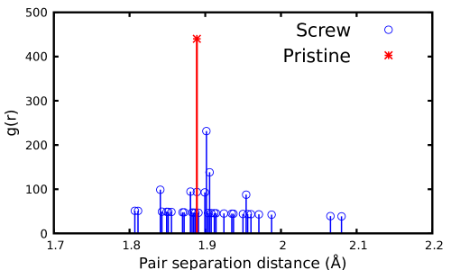
In Fig. 7 we show the radial pair distribution function, , of both the pristine 3C-SiC supercell and that of its dislocated counterpart. As can be seen, the bulk case is characterized by a single nearest neighbour distance. However, once the dislocation dipole is created, the bonding distribution of the supercell exhibits a disorder that explain both the band tail states and the symmetry breaking that lifts the degeneracy of the states associated to the neutral DV.
References
- Nielsen and Chuang (2010) M. Nielsen and I. Chuang, Quantum Computation and Quantum Information: 10th Anniversary Edition (Cambridge University Press, 2010).
- Ladd et al. (2010) T. D. Ladd, F. Jelezko, R. Laflamme, Y. Nakamura, C. Monroe, and J. L. O’Brien, Nature 464, 45 (2010).
- Flamini et al. (2018) F. Flamini, N. Spagnolo, and F. Sciarrino, Reports on Progress in Physics 82, 016001 (2018).
- Slussarenko and Pryde (2019) S. Slussarenko and G. J. Pryde, Applied Physics Reviews 6, 041303 (2019).
- Häffner et al. (2008) H. Häffner, C. Roos, and R. Blatt, Physics Reports 469, 155 (2008).
- Bruzewicz et al. (2019) C. D. Bruzewicz, J. Chiaverini, R. McConnell, and J. M. Sage, Applied Physics Reviews 6, 021314 (2019).
- Gruber et al. (1997) A. Gruber, A. Dräbenstedt, C. Tietz, L. Fleury, J. Wrachtrup, and C. von Borczyskowski, Science 276, 2012 (1997).
- Balasubramanian et al. (2009) G. Balasubramanian, P. Neumann, D. Twitchen, M. Markham, R. Kolesov, N. Mizuochi, J. Isoya, J. Achard, J. Beck, J. Tissler, V. Jacques, P. R. Hemmer, F. Jelezko, and J. Wrachtrup, Nature Materials 8, 383 (2009).
- Doherty et al. (2013) M. W. Doherty, N. B. Manson, P. Delaney, F. Jelezko, J. Wrachtrup, and L. C. Hollenberg, Physics Reports 528, 1 (2013), the nitrogen-vacancy colour centre in diamond.
- Zhang et al. (2020) G. Zhang, Y. Cheng, J.-P. Chou, and A. Gali, Applied Physics Reviews 7, 031308 (2020).
- Chatterjee et al. (2021) A. Chatterjee, P. Stevenson, S. De Franceschi, A. Morello, N. P. de Leon, and F. Kuemmeth, Nature Reviews Physics 3, 157 (2021).
- Wolfowicz et al. (2021) G. Wolfowicz, F. J. Heremans, C. P. Anderson, S. Kanai, H. Seo, A. Gali, G. Galli, and D. D. Awschalom, Nature Reviews Materials 6, 906 (2021).
- Koehl et al. (2015) W. F. Koehl, H. Seo, G. Galli, and D. D. Awschalom, MRS Bulletin 40, 1146–1153 (2015).
- Atatüre et al. (2018) M. Atatüre, D. Englund, N. Vamivakas, S.-Y. Lee, and J. Wrachtrup, Nature Reviews Materials 3, 38 (2018).
- Schröder et al. (2017) T. Schröder, M. E. Trusheim, M. Walsh, L. Li, J. Zheng, M. Schukraft, A. Sipahigil, R. E. Evans, D. D. Sukachev, C. T. Nguyen, J. L. Pacheco, R. M. Camacho, E. S. Bielejec, M. D. Lukin, and D. Englund, Nature Communications 8, 15376 (2017).
- Wang et al. (2017) J. Wang, Y. Zhou, X. Zhang, F. Liu, Y. Li, K. Li, Z. Liu, G. Wang, and W. Gao, Phys. Rev. Applied 7, 064021 (2017).
- Zhou et al. (2018) Y. Zhou, Z. Mu, G. Adamo, S. Bauerdick, A. Rudzinski, I. Aharonovich, and W. bo Gao, New Journal of Physics 20, 125004 (2018).
- Chen et al. (2019) Y.-C. Chen, B. Griffiths, L. Weng, S. S. Nicley, S. N. Ishmael, Y. Lekhai, S. Johnson, C. J. Stephen, B. L. Green, G. W. Morley, M. E. Newton, M. J. Booth, P. S. Salter, and J. M. Smith, Optica 6, 662 (2019).
- Smith et al. (2019) J. M. Smith, S. A. Meynell, A. C. B. Jayich, and J. Meijer, Nanophotonics 8, 1889 (2019).
- Castelletto and Boretti (2020) S. Castelletto and A. Boretti, Journal of Physics: Photonics 2, 022001 (2020).
- Kumar et al. (2015) S. Kumar, A. Kaczmarczyk, and B. D. Gerardot, Nano Letters 15, 7567 (2015).
- Branny et al. (2017) A. Branny, S. Kumar, R. Proux, and B. D. Gerardot, Nature Communications 8, 15053 (2017).
- Weber et al. (2010) J. R. Weber, W. F. Koehl, J. B. Varley, A. Janotti, B. B. Buckley, C. G. V. de Walle, and D. D. Awschalom, Proceedings of the National Academy of Sciences 107, 8513 (2010).
- Stamp and Gaita-Ariño (2009) P. C. E. Stamp and A. Gaita-Ariño, J. Mater. Chem. 19, 1718 (2009).
- Bassett et al. (2019) L. C. Bassett, A. Alkauskas, A. L. Exarhos, and K.-M. C. Fu, Nanophotonics 8, 1867 (2019).
- Kaviani et al. (2014) M. Kaviani, P. Deák, B. Aradi, T. Frauenheim, J.-P. Chou, and A. Gali, Nano Letters 14, 4772 (2014).
- Chou and Gali (2017) J.-P. Chou and A. Gali, MRS Communications 7, 551–562 (2017).
- Chou et al. (2017) J.-P. Chou, A. Retzker, and A. Gali, Nano Letters 17, 2294 (2017).
- Stacey et al. (2019) A. Stacey, N. Dontschuk, J.-P. Chou, D. A. Broadway, A. K. Schenk, M. J. Sear, J.-P. Tetienne, A. Hoffman, S. Prawer, C. I. Pakes, A. Tadich, N. P. de Leon, A. Gali, and L. C. L. Hollenberg, Advanced Materials Interfaces 6, 1801449 (2019).
- Sangtawesin et al. (2019) S. Sangtawesin, B. L. Dwyer, S. Srinivasan, J. J. Allred, L. V. H. Rodgers, K. De Greve, A. Stacey, N. Dontschuk, K. M. O’Donnell, D. Hu, D. A. Evans, C. Jaye, D. A. Fischer, M. L. Markham, D. J. Twitchen, H. Park, M. D. Lukin, and N. P. de Leon, Phys. Rev. X 9, 031052 (2019).
- Li et al. (2019) S. Li, J.-P. Chou, J. Wei, M. Sun, A. Hu, and A. Gali, Carbon 145, 273 (2019).
- Shen et al. (2020) W. Shen, S. Shen, S. Liu, H. Li, Z. Gan, and Q. Zhang, ACS Applied Materials & Interfaces 12, 33336 (2020).
- Körner et al. (2021) W. Körner, D. F. Urban, and C. Elsässer, Phys. Rev. B 103, 085305 (2021).
- Körner et al. (2022) W. Körner, R. Ghassemizadeh, D. F. Urban, and C. Elsässer, Phys. Rev. B 105, 085305 (2022).
- Löfgren et al. (2022) R. Löfgren, S. Öberg, and J. A. Larsson, AIP Advances 12, 035009 (2022).
- Dwyer et al. (2022) B. L. Dwyer, L. V. Rodgers, E. K. Urbach, D. Bluvstein, S. Sangtawesin, H. Zhou, Y. Nassab, M. Fitzpatrick, Z. Yuan, K. De Greve, E. L. Peterson, H. Knowles, T. Sumarac, J.-P. Chou, A. Gali, V. Dobrovitski, M. D. Lukin, and N. P. de Leon, PRX Quantum 3, 040328 (2022).
- Ivády et al. (2019) V. Ivády, J. Davidsson, N. Delegan, A. L. Falk, P. V. Klimov, S. J. Whiteley, S. O. Hruszkewycz, M. V. Holt, F. J. Heremans, N. T. Son, D. D. Awschalom, I. A. Abrikosov, and A. Gali, Nature Communications 10, 5607 (2019).
- Holt and Yacobi (2007) D. Holt and B. Yacobi, Extended Defects in Semiconductors: Electronic Properties, Device Effects and Structures (Cambridge University Press, 2007).
- Hull and Bacon (2011) D. Hull and D. Bacon, Introduction to Dislocations, Materials science and technology (Elsevier Science, 2011).
- Cai et al. (2016) W. Cai, W. Nix, and M. R. Society, Imperfections in Crystalline Solids, MRS-Cambridge Materials Fundamentals (Cambridge University Press, 2016).
- Anderson et al. (2017) P. Anderson, J. Hirth, and J. Lothe, Theory of Dislocations (Cambridge University Press, 2017).
- Ghassemizadeh et al. (2022) R. Ghassemizadeh, W. Körner, D. F. Urban, and C. Elsässer, Phys. Rev. B 106, 174111 (2022).
- Reiche et al. (2010) M. Reiche, M. Kittler, D. Buca, A. Hähnel, Q.-T. Zhao, S. Mantl, and U. Gösele, Japanese Journal of Applied Physics 49, 04DJ02 (2010).
- Reiche et al. (2014) M. Reiche, M. Kittler, W. Erfurth, E. Pippel, K. Sklarek, H. Blumtritt, A. Haehnel, and H. Uebensee, Journal of Applied Physics 115, 194303 (2014).
- Stukowski (2010) A. Stukowski, Modelling and Simul. Mater. Sci. Eng. 18, 015012 (2010).
- Pizzagalli et al. (2005) L. Pizzagalli, P. Beauchamp, and J. Rabier, Europhysics Letters 72, 410 (2005).
- Demenet et al. (2013) J.-L. Demenet, M. Amer, C. Tromas, D. Eyidi, and J. Rabier, physica status solidi c 10, 64 (2013).
- Pizzagalli (2014) L. Pizzagalli, Acta Materialia 78, 236 (2014).
- Christle et al. (2017) D. J. Christle, P. V. Klimov, C. F. de las Casas, K. Szász, V. Ivády, V. Jokubavicius, J. Ul Hassan, M. Syväjärvi, W. F. Koehl, T. Ohshima, N. T. Son, E. Janzén, A. Gali, and D. D. Awschalom, Phys. Rev. X 7, 021046 (2017).
- Son et al. (2020) N. T. Son, C. P. Anderson, A. Bourassa, K. C. Miao, C. Babin, M. Widmann, M. Niethammer, J. Ul Hassan, N. Morioka, I. G. Ivanov, F. Kaiser, J. Wrachtrup, and D. D. Awschalom, Applied Physics Letters 116, 190501 (2020).
- Bulatov and Cai (2006) V. Bulatov and W. Cai, Computer Simulations of Dislocations, OSMM (OUP Oxford, 2006).
- Rodney et al. (2017) D. Rodney, L. Ventelon, E. Clouet, L. Pizzagalli, and F. Willaime, Acta Materialia 124, 633 (2017).
- Clouet (2020) E. Clouet, “Ab initio models of dislocations,” in Handbook of Materials Modeling: Methods: Theory and Modeling, edited by W. Andreoni and S. Yip (Springer International Publishing, Cham, 2020) pp. 1503–1524.
- (54) E. Clouet, Babel package. Available online at URL http://emmanuel.clouet.free.fr/Programs/Babel/ .
- Kresse and Furthmüller (1996) G. Kresse and J. Furthmüller, Phys. Rev. B 54, 11169 (1996).
- Li and Bradt (1986) Z. Li and R. C. Bradt, Journal of Materials Science 21, 4366 (1986).
- Perdew et al. (1996) J. P. Perdew, K. Burke, and M. Ernzerhof, Phys. Rev. Lett. 77, 3865 (1996).
- Heyd et al. (2003) J. Heyd, G. E. Scuseria, and M. Ernzerhof, The Journal of Chemical Physics 118, 8207 (2003), https://doi.org/10.1063/1.1564060 .
- Heyd et al. (2006) J. Heyd, G. E. Scuseria, and M. Ernzerhof, The Journal of Chemical Physics 124, 219906 (2006), https://doi.org/10.1063/1.2204597 .
- Freysoldt et al. (2014) C. Freysoldt, B. Grabowski, T. Hickel, J. Neugebauer, G. Kresse, A. Janotti, and C. G. Van de Walle, Rev. Mod. Phys. 86, 253 (2014).
- Komsa et al. (2012) H.-P. Komsa, T. T. Rantala, and A. Pasquarello, Phys. Rev. B 86, 045112 (2012).
- Freysoldt et al. (2009) C. Freysoldt, J. Neugebauer, and C. G. Van de Walle, Phys. Rev. Lett. 102, 016402 (2009).
- Momma and Izumi (2011) K. Momma and F. Izumi, J. Appl. Cryst. 44, 1272 (2011).
- Gordon et al. (2015) L. Gordon, A. Janotti, and C. G. Van de Walle, Phys. Rev. B 92, 045208 (2015).
- Schultz et al. (2021) P. A. Schultz, R. M. Van Ginhoven, and A. H. Edwards, Phys. Rev. B 103, 195202 (2021).
- Lee et al. (2000) S. M. Lee, M. A. Belkhir, X. Y. Zhu, Y. H. Lee, Y. G. Hwang, and T. Frauenheim, Phys. Rev. B 61, 16033 (2000).
- Barragan-Yani and Albe (2017) D. Barragan-Yani and K. Albe, Phys. Rev. B 95, 115203 (2017).
- Aschauer and Spaldin (2016) U. Aschauer and N. A. Spaldin, Applied Physics Letters 109, 031901 (2016).
- Simsek Sanli et al. (2017) E. Simsek Sanli, D. Barragan-Yani, Q. M. Ramasse, K. Albe, R. Mainz, D. Abou-Ras, A. Weber, H.-J. Kleebe, and P. A. van Aken, Phys. Rev. B 95, 195209 (2017).
- Csóré et al. (2022) A. Csóré, N. Mukesh, G. Károlyházy, D. Beke, and A. Gali, Journal of Applied Physics 131, 071102 (2022).
- Gao et al. (2022) W. Gao, F. H. da Jornada, M. Del Ben, J. Deslippe, S. G. Louie, and J. R. Chelikowsky, Phys. Rev. Mater. 6, 036201 (2022).
- Stukowski and Albe (2010) A. Stukowski and K. Albe, Modelling and Simulation in Materials Science and Engineering 18, 025016 (2010).