PROBE3.0: A Systematic Framework for Design-Technology Pathfinding with Improved Design Enablement
Abstract
We propose a systematic framework to conduct design-technology pathfinding for PPAC in advanced nodes. Our goal is to provide configurable, scalable generation of process design kit (PDK) and standard-cell library, spanning key scaling boosters (backside PDN and buried power rail), to explore PPAC across given technology and design parameters. We build on [6], which addressed only area and cost (AC), to include power and performance (PP) evaluations through automated generation of full design enablements. We also improve the use of artificial designs in the PPAC assessment of technology and design configurations. We generate more realistic artificial designs by applying a machine learning-based parameter tuning flow to [16]. We further employ clustering-based cell width-regularized placements at the core of routability assessment, enabling more realistic placement utilization and improved experimental efficiency. We demonstrate PPAC evaluation across scaling boosters and artificial designs in a predictive technology node.
I Introduction
Due to the slowdown of dimension scaling relative to the trend of the traditional Moore’s Law, scaling boosters, such as backside power delivery networks (BSPDN), buried power rails (BPR), are introduced at advanced technology nodes. Since scaling boosters play an important role to optimize power, performance, area and cost (PPAC) of advanced technologies, accurate and fast evaluations and predictions of PPAC are critical at an early stage of technology development. Also, use of scaling boosters makes evaluations and predictions of technology more difficult since they introduce a large number of knobs to contribute PPAC improvement.
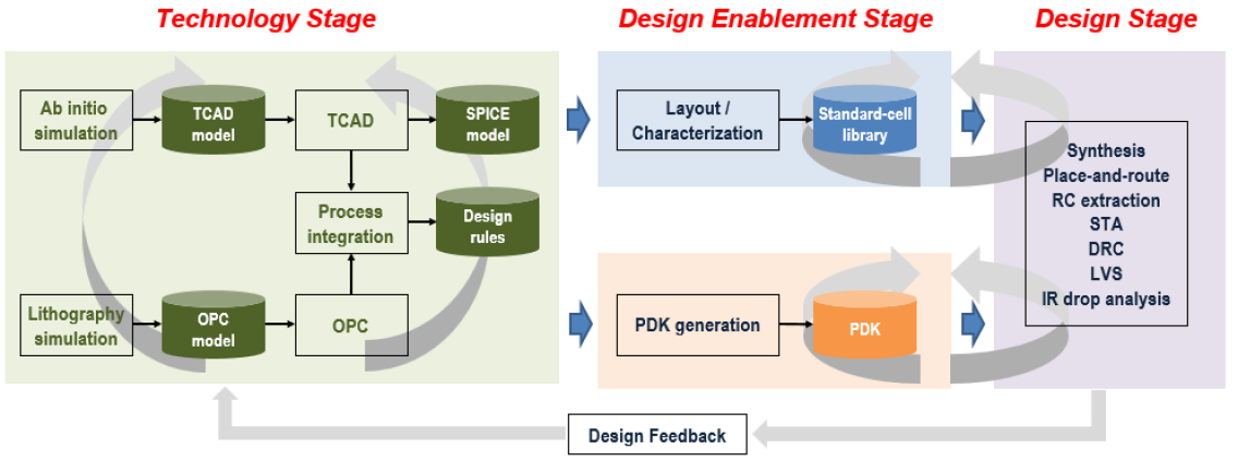
Design-Technology Co-Optimization (DTCO) is now a well-known key element to develop advanced technology nodes and designs in the modern VLSI chip design. Today’s DTCO spans assessment and co-optimization across almost all components of semiconductor technology and design enablement. As described in Figure 1, the DTCO process consists of three stages: Technology, Design Enablement, and Design. First, the technology stage includes modeling and simulation methodologies for process and device technology. Second, the design enablement stage includes creation of required process design kits (PDK) for the ensuing design stage; these include device models, standard-cell libraries, routing technology files and interconnect parasitic (RC) models. Last, the design stage includes logic synthesis and place-and-route (P&R) based on the generated PDKs from the design enablement stage.
To evaluate and predict technology and design at advanced nodes, all three stages must be correctly performed, and PDKs must be generated from technology and design enablement stages. However, the DTCO process is not simple: feedback from design stage to technology stage takes weeks to months of turnaround time, along with immense engineering efforts. Also, based on the design feedback, additional PDKs may need to be generated at the design enablement stage, which requires additional weeks to months. In order to reduce the turnaround time and maximize the benefit of the DTCO process, a fast and accurate DTCO methodology is needed to assess PPAC with reasonable turnaround time, and to more precisely guide multi-million dollar decisions at an early stage of technology development.
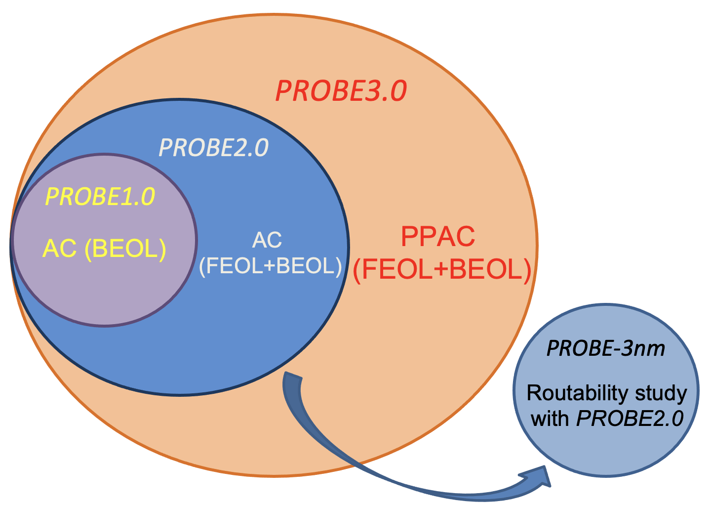
Contributions of Our Work. Compared to the previous works PROBE1.0 [13] and PROBE2.0 [6], our new framework provides three main technical achievements.
(1) We establish the first comprehensive end-to-end design and technology pathfinding framework. [6][13] focus on area and cost without considering power and performance. Thus, there is a significant discrepancy between [6][13] and the actual DTCO process in the industry. In this work, we propose a more complete and systematic PROBE3.0 framework, which incorporates power and performance aspects for design-technology pathfinding at an early stage of technology development. PROBE3.0 enables fast and accurate PPAC evaluations by generating configurable PDKs, including standard-cell libraries.
(2) We improve our designs for PPAC explorations. Design is a critical factor for PPAC explorations, and artificially generated designs enable us to explore a wider solution space. We leverage [16] to generate artificial designs. To create more realistic artificial designs, we develop a machine learning (ML)-based parameter tuning flow built on [16] to find the best input parameters for generating such designs. Section V details our artificial design generation flow. Further, cell width-regularization is employed in [6][13] to prevent illegal placements when swapping neighboring cells to assess the routability metric, . We propose a clustering-based cell width-regularization to achieve more realistic utilization (and faster routability assessment) as described in Section VI.
(3) We demonstrate the PPAC exploration of scaling boosters. We incorporate scaling boosters (BSPDN and BPR) to support P&R and IR drop analysis flows within the framework, as detailed in Section IV. Our results show that incorporating BSPDN and BPR leads to a reduction in power consumption by up to 8% and area by up to 24% based on our predictive 3nm technology. The area reduction results are consistent with those reported in previous industry works [10][22][29][31], which have demonstrated area reductions of 25% to 30% through the use of BSPDN and BPR techniques.
Due to limited access to advanced technology for academic research, we build our predictive 3nm technology, named the PROBE3.0 technology. To calibrate the technology, we refer to the International Roadmap for Devices and Structures (IRDS) [40], open-sourced PDKs, and other publications [2][8][23][37]. We open-source our work, including process design kits (PDKs), standard-cell libraries, and scripts for P&R and IR drop analysis; this is available in our GitHub repository [48]. In Section III, we provide details on the automated PDKs and library generation flows, while in Section VII, we present three experiments to demonstrate the effectiveness of the PROBE3.0 framework for PPAC pathfinding.
II Related Work
In this section, we divide the relevant previous works into the three categories of (i) advanced-technology research PDKs, (ii) design-technology co-optimization and (iii) scaling boosters, along with (iv) “PROBE” frameworks.
Advanced Technology Research PDKs. PDKs of advanced node technologies are highly confidential. Academic research can be blocked by limited access to relevant information. To unblock academic research, predictive advanced-node PDKs have been published. ASAP7 [8] is a predictive PDK for 7nm FinFET technology that includes standard cells which support commercial logic synthesis and P&R. FreePDK3 [23][37] and FreePDK15 [2] are open-source PDKs for 3nm and 15nm technology. [15] proposes a 3nm predictive technology called NS3K with nanosheet FETs (NSFET). The authors of [15] also create 5nm FinFET and 3nm NSFET libraries to compare power, performance and area.
Design-Technology Co-Optimization. Previous DTCO works evaluate block-level PPAC and optimize design and technology simultaneously. [25] proposes UTOPIA to evaluate block-level PPAC with thermally limited performance, and to optimize device and technology parameters. [18] proposes a fast pathfinding DTCO flow for FinFET and complementary FET (CFET). [3] also proposes a fast and agile technology pathfinding platform with compact device models to accelerate the DTCO process. [12] describes power delivery network pathfinding for 3D IC technology to study tradeoffs between IR drop and routability. [5] uses ML to predict sensitivities to changes for DTCO.
Scaling Boosters. As described in Section I, scaling boosters are used in advanced nodes to maximize benefit of new technology. BSPDN and BPR are among the most promising scaling boosters in sub-5nm nodes. [21] carries out a CPU implementation with BSPDN and BPR in their 3nm technology, demonstrating a reduction of up to 7X in worst IR drop. Similarly, [22] investigates BSPDN and BPR at sub-3nm nodes and finds that they can lead to a 30% reduction in area based on IR drop mitigation. [4] also explores the impact of BSPDN and BPR on design, concluding that their use can lead to a 43% reduction in area with 4X less IR drop. [10] studies BSPDN configurations with TSVs, and observes 25% to 30% reduction in area using BSPDN and BPR. Additionally, [24] investigates BSPDN with nTSVs and TSVs and finds that the average IR drop with BSPDN improves by 69% compared to traditional frontside PDN (FSPDN). Finally, [27] conducts holistic evaluations for BSPDN and BPR, demonstrating that FSPDN with BPR achieves a 25% lower on-chip IR drop, while BSPDN with BPR achieves an 85% lower on-chip IR drop with iso-performance and iso-area. In contrast to these previous DTCO works, here we propose a highly configurable framework that enables more efficient investigation of scaling boosters in advanced nodes.
“PROBE” Frameworks. Prior “PROBE” [6][13] works propose systematic frameworks for assessing routability with different FEOL and BEOL configurations. Specifically, [13] begins with an easily-routable placement and increases the routing difficulty by random neighbor-swaps until the routing fails with greater than a threshold number of design rule violations (DRCs). The normalized number of swaps at which routing failure occurs, denoted by , is a metric used to measure the inherent routability of the given parameters. On the other hand, [6] introduces an automatic standard-cell layout generation using satisfiability modulo theory (SMT) to support explorations of both FEOL and BEOL configurations. The authors of [6] also employ machine learning (ML)-based prediction to expedite the DTCO pathfinding process. Additionally, [7] employs PROBE2.0 in a routability study with sub-3nm technology configurations.
III Standard-Cell Library and PDK Generation
Expediting the DTCO process requires automation of the standard-cell library and PDK generation flows. Therefore, the PROBE2.0 framework [6] introduces standard-cell layout and PDK generation flows and utilizes them for routability assessments. In this work, we extend the PROBE2.0 framework to include proper electrical models of standard-cell libraries and interconnect layers for design-technology pathfinding. Additionally, we enhance the PDK generation flow to support advanced nodes. While the PROBE2.0 framework solely focuses on the physical layout of standard cells, the PROBE3.0 framework enables true full-stack PPAC pathfinding through automated, configurable standard-cell and PDK generation flows for advanced nodes. To demonstrate use of PROBE3.0 for advanced-node PPAC pathfinding, we use a technology that incorporates cutting-edge (3nm FinFET) technology predictions based on the works of [8][40].
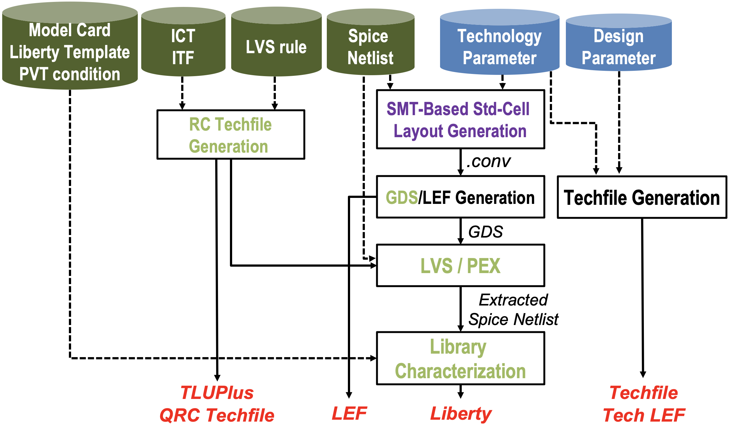
III-A Overall flow
Figure 3 describes our overall flow of standard-cell and PDK generation. Technology and design parameters are defined as input parameters for the flow. Beyond these input parameters, there are additional inputs required to generate standard-cell libraries and PDKs, as follows: (i) SPICE model cards, (ii) Liberty template and PVT conditions, (iii) Interconnect technology files (ICT/ITF), (iv) LVS rule deck, and (v) SPICE netlists. Given the inputs, our SMT-based standard-cell layout generation and GDS/LEF generation are executed sequentially. Generation of timing and power models (Liberty) requires additional steps including LVS, parasitic extraction and library characterization flow. Aside from the standard-cell library generation, we also generate interconnect models from ICT/ITF, and P&R routing technology files from technology and design parameters. The PDK elements that we generate feed seamlessly into commercial logic synthesis and P&R tools. Further, to the best of our knowledge, ours is the first-ever work that is able to disseminate all associated EDA tool scripts for research purposes.
III-B PROBE3.0 Technology
We build our own predictive 3nm technology node, called the PROBE3.0 technology. Based on [8], we define our FEOL and BEOL layers as described in Table I. We assume that all BEOL layers are unidirectional routing layers. Hence, we first change M1 to a unidirectional routing layer with vertical preferred direction, since the work of [8] has a bidirectional M1 routing layer. We add an M0 layer with horizontal preferred direction below the modified M1 layer, and we add contact layers V0 and CA which respectively connect between M1 and M0, and between gate/source-drain and M0.
| Layer | Name | Description |
|---|---|---|
| FEOL | WELL | N-Well |
| FIN | Fin | |
| GATE | Poly (gate) | |
| GCUT | Gate cut | |
| ACTIVE | Active area for fin definition | |
| NSELECT | N-implant | |
| PSELECT | P-implant | |
| CA | Contact (via) between LIG/LISD and M0 | |
| LIG | Gate interconnect layer | |
| LISD | Source-drain interconnect layer | |
| SDT | Source-drain trench (ACTIVE to LIG/LISD) | |
| BOUNDARY | Boundary layer for P&R | |
| BEOL | M0-M13 | Metal layers |
| V0-V12 | Via layers |
Also, electrical features of technologies are critical to explore “PP” aspects. Therefore, parasitic extractions of standard cells and BEOL metal stacks are important steps. To extract parasitic elements, interconnect technology files are required to use commercial RC extraction, P&R and IR drop analysis tools. In this work, we use commercial tools [35][43][46] for extractions, and each tool has its own technology file format.111The file formats for each tool are unique. The MIPT file format is for Siemens Calibre [43] for extraction, and is converted to an RC rule file for standard-cell layout extractions. On the other hand, the ICT and ITF file formats are for Cadence and Synopsys extraction tools, respectively. We convert ICT to QRC techfile, and ITF to TLUPlus file, to enable P&R tools and IR drop analysis. Interconnect technology files include layer structures of technology and electrical parameters, such as thickness, width, resistivity, dielectric constant and via resistance. We refer to the values of physical features in the 3nm FinFET technology of [40], such as fin pitch, fin width, gate pitch, gate width, metal pitch and aspect ratio. We also refer to [40] for the values for electrical parameters such as via resistance and dielectric constant. Table II describes key features of the PROBE3.0 technology.
| Layer | Feature | Value |
|---|---|---|
| FEOL | Fin Pitch | 24 nm |
| Fin Width | 6 nm | |
| Gate Pitch (CPP) | 45 nm | |
| Gate Width | 16 nm | |
| Standard-Cell Height | 100 / 120 / 144 nm | |
| Dielectric constant | 3.9 | |
| BEOL | Aspect Ratio (width/thickness) | 1.5 |
| Power/Ground Pin Width (M0) | 36 nm | |
| M0/M2/M3 pitch | 24 nm | |
| M1 pitch | 30 nm | |
| M4-M11 pitch | 64 nm | |
| M12-M13 / BM1-BM2 pitch | 720 nm | |
| V0-V3 via resistance | 50 ohm/via | |
| V4-V11 via resistance | 5 ohm/via | |
| V12 via resistance | 0.06294 ohm/via | |
| Dielectric constant | 2.5-3 |
III-C Improved Standard-Cell Library Generation
We generate standard-cell libraries via several steps illustrated in Figure 3: (i) SMT-based standard-cell layout generation, (ii) generation of GDS and LEF files, (iii) LVS and PEX flow, and (iv) library characterization flow.
SMT-Based Standard-Cell Layout Generation. In recent technology nodes, standard-cell architectures use a variety of pitch values for different layers in order to optimize power, performance, area and cost (PPAC). To accommodate this, PROBE3.0 improves the SMT-based layout generation used in PROBE2.0 to support non-unit gear ratios for M1 pitch (M1P) and contacted poly pitch (CPP).
Our standard-cell layouts are generated using SPICE netlists, technology and design parameters from [6]. However, in PROBE3.0 we change two key parameters: metal pitch (MP) and power delivery network (PDN). Instead of using MP, we define parameters for pitch values of each layer. Since M0, M1 and M2 layers are used for standard-cell layouts, we define M0P, M1P and M2P as pitches of M0, M1 and M2 layers, respectively. Table 4 shows four layouts of AND2_X1 cells with four parameter settings. The four standard-cell libraries (Lib1, Lib2, Lib3 and Lib4) along with their corresponding parameter sets are used for our experiments in Section VII. For our PPAC exploration, we generate 41 standard cells for each standard-cell library as shown in Table III.
GDS/LEF Generation and LVS/PEX Flow. While [6] only supports LEF generation for P&R, PROBE3.0 generates standard-cell layouts in both GDS and LEF formats. The GDS files are used to extract parasitics from standard-cell layouts and check LVS between layouts and schematics. We use Calibre [43] to check LVS and generate extracted netlists for standard cells with intra-cell RC parasitics. Scripts for GDS/LEF generation and LVS/PEX flows are open-sourced in [48].
Library Characterization Flow. We perform library characterization to generate standard-cell libraries in the Liberty format. The inputs to the flow are model cards for FinFET devices, Liberty template including PVT conditions, and interconnect technology files. We use model cards from [37]. For the Liberty template, we define the PVT conditions, and the capacitance and transition time indices of (77) tables for electrical models (delay, output transition time, and power). We use 5, 10, 20, 40, 80, 160, and 320 as the transition time indices. For the input capacitance, we obtain the input pin capacitance of an X1 inverter, then multiply this value by predefined multipliers, 2, 4, 8, 16, 24, 32, and 64. For characterization, we use the PVT corner ().
| Cell List | Size |
|---|---|
| Inverter (INV), Buffer (BUF) | X1, X2, X4, X8 |
| 2-input AND/OR/NAND/NOR (AND2/OR2/NAND2/NOR2) | X1, X2 |
| 3-input AND/OR/NAND/NOR (AND3/OR3/NAND3/NOR3) | X1, X2 |
| 4-input NAND/NOR (NAND4/NOR4) | X1, X2 |
| 2-1 AND-OR-Inverter (AOI21), 2-2 AND-OR-Inverter (AOI22) | X1, X2 |
| 2-1 OR-AND-Inverter (OAI21), 2-2 OR-AND-Inverter (OAI22) | X1, X2 |
| D flip-flop (DFFHQN), D flip-flop with reset (DFFRNQ) | X1 |
| 2-input MUX/XOR (MUX2/XOR2), Latch (LHQ) | X1 |
IV Power Delivery Network
We study PDN scaling boosters to showcase the DTCO and pathfinding capability of PROBE3.0. There are two key challenges of traditional PDNs at advanced technologies:
-
•
High resistance of BEOL [19]: Elevated resistance in BEOL layers exacerbates IR drop issues, necessitating denser PDN topologies.
-
•
Routing overheads (routability) [26]: PDN occupies routing resources that are shared with signal and clock distribution. The routability and area density impact of PDN becomes more severe with denser PDN at advanced nodes.
To overcome these challenges, multiple foundries have begun implementing backside power delivery networks (BSPDN) and buried power rails (BPR) as scaling boosters in their sub-5nm technologies. We use these scaling boosters, BSPDN and BPR, to demonstrate use of PROBE3.0. We establish four options for parameter in the PROBE3.0 framework: (i) Frontside PDN without BPR (); (ii) Frontside PDN with BPR (); (iii) Backside PDN without BPR (); and (iv) Backside PDN with BPR (). Figure 5 illustrates the four PDN configurations in the PROBE3.0 framework.
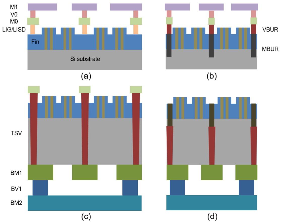
IV-A Frontside and Backside Power Delivery Network
We have defined realistic structures for both frontside power delivery networks (FSPDN) and backside power delivery networks (BSPDN), and enabled IR drop analysis within our framework. Table IV shows the configurations for FSPDN and BSPDN. Since BEOL layers with smaller pitches (e.g., 24nm-pitch layer) have high resistance, we add power stripes for every layer. While the work of [6] has multiple options for FSPDN, the PROBE3.0 framework has only one PDN structure for FSPDN. Instead, we add other options such as , and . Furthermore, while the Backside option in [6] assumes no PDN at the frontside for the BSPDN option, we add power stripes at the backside for BSPDN in the PROBE3.0 framework to enable IR drop analysis for BSPDN.
| PDN | Layer | Pitch | Width | Spacing | Density |
| (um) | (um) | (um) | (%) | ||
| FSPDN | M3 | 1.08 | 0.012 | 0.508 | 4 |
| M4 | 1.152 | 0.032 | 0.544 | 11 | |
| M5-M11 | 5.0 | 1.0 | 1.5 | 20 | |
| M12-M13 | 4.32 | 1.8 | 0.36 | 100 | |
| BSPDN | BM1-BM2 | 4.32 | 1.8 | 0.36 | 100 |
Figures 5(a) and (c) respectively show cross-section views of and options. The option has M0 power and ground pins for standard cells, which connect to power stripes at the frontside of the die. The option uses the same M0 power and ground pins for standard cells but connects to power stripes at the backside of the die. For the option, we employ two backside metal layers (BM1 and BM2) and one via layer (BV1) between the backside metal layers. The layer characteristics (width, pitch and spacing) are identical to the top two layers (M12 and M13) of FSPDN. Additionally, the M0 pins of standard cells and BSPDN are connected using Through-Silicon Vias (TSVs). We assume nano-TSVs with 90nm [24] width for the option, and 1:10 width-to-height aspect ratio. For the option, TSV insertions necessitate reserved spaces in front-end-of-line (FEOL) layers, including keepout margins surrounding the TSVs. To accommodate this, we insert power tap cells prior to standard-cell placement.
IV-B Frontside and Backside PDN with Buried Power Rail
In advanced nodes, power rails on BEOL metal layers can be “buried” into FEOL levels with shallow-trench isolation (STI). Using deep trench and creating space between devices lowers the resistance of power rails. In addition to the resistance benefits, standard-cell height (area) can be further reduced with deep and narrow widths of power and ground pins. Figures 5(b) and (d) respectively show cross-section views of FSPDN with BPR () and BSPDN with BPR () options. In the case of , connections between FSPDN and BPR are made through nano-TSVs with the same 90nm width as in the option (but, with 1:7 aspect ratio). These nano-TSVs also necessitate insertion of reserved spaces.
IV-C Power Tap Cell Insertion
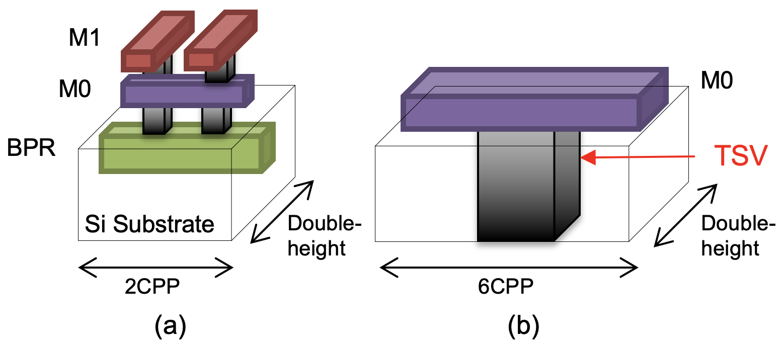
Although use of BSPDN and BPR can reduce area and mitigate IR drop problems, connecting frontside layers to BSPDN and/or BPR remains a critical challenge. To establish “tap” connections from frontside metals to BPR, or from backside to frontside metals, space must be reserved on device layers – e.g., [21] proposes power tap cells for the connection between BPR to MINT (M0) layers. More frequent “taps” will mitigate IR drop problems, but occupy more placement area. In PROBE3.0, we define two types of power tap cells for the and options. Tap cells for connect BPR to M1, and tap cells for connect BM1 to M0. By contrast, and do not require power tap cells.
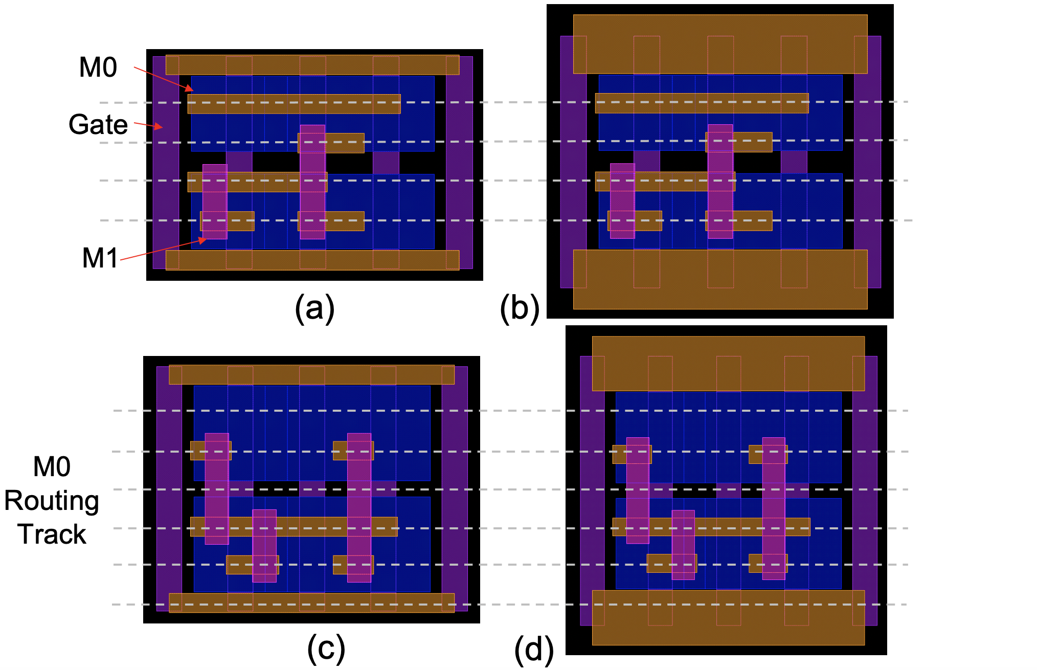
Power Tap Cell Structure. Figure 6(a) shows a structure of power tap cells for . Double-height power tap cells for have 2CPP cell width. The connection between BPR and M0 is through a 12 via array, and the two M1 metals are aligned with M1 vertical routing tracks. There are also two types of power tap cells for according to starting power and ground pins: power/ground pins on the double-height power tap cells are ordered as Power-Ground-Power (VDD-VSS-VDD) or Ground-Power-Ground (VSS-VDD-VSS). On the other hand, Figure 6(b) shows a structure of power tap cells for . While power tap cells for have 2CPP width, double-height power tap cells for have 6CPP width due to the 90nm width of nano-TSVs [24]. We also assume a 50nm keepout spacing around nano-TSVs. Similar to power tap cells for , there are two types of double-height power tap cells for , Power-Ground-Power and Ground-Power-Ground.
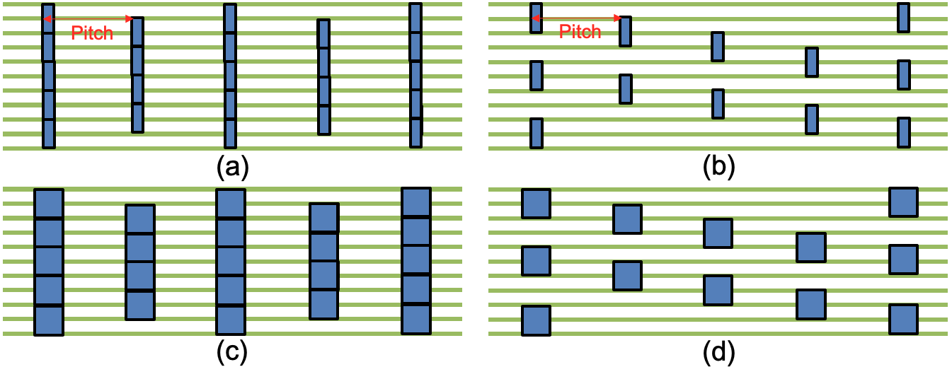
Power Tap Cell Insertion Scheme. Power tap cell insertion affects routability and IR drop, and hence affect PPAC of designs. In this work, we define five tap cell insertion pitches and two power tap insertion schemes, as follows.
-
•
: 24, 32, 48, 96 and 128CPP
-
•
: Column and Staggered
and denote tap cell insertion pitch and tap cell insertion scheme, respectively. Tap cell insertion scheme Column places double-height power tap cells on every two placement rows with the given tap cell pitch. Conversely, tap cell insertion scheme Staggered places double-height power tap cells on every four placement rows with the given tap cell pitch. Figure 7 shows four power tap cell insertion results for and with Column and Staggered insertion schemes.
IV-D IR Drop Analysis Flow
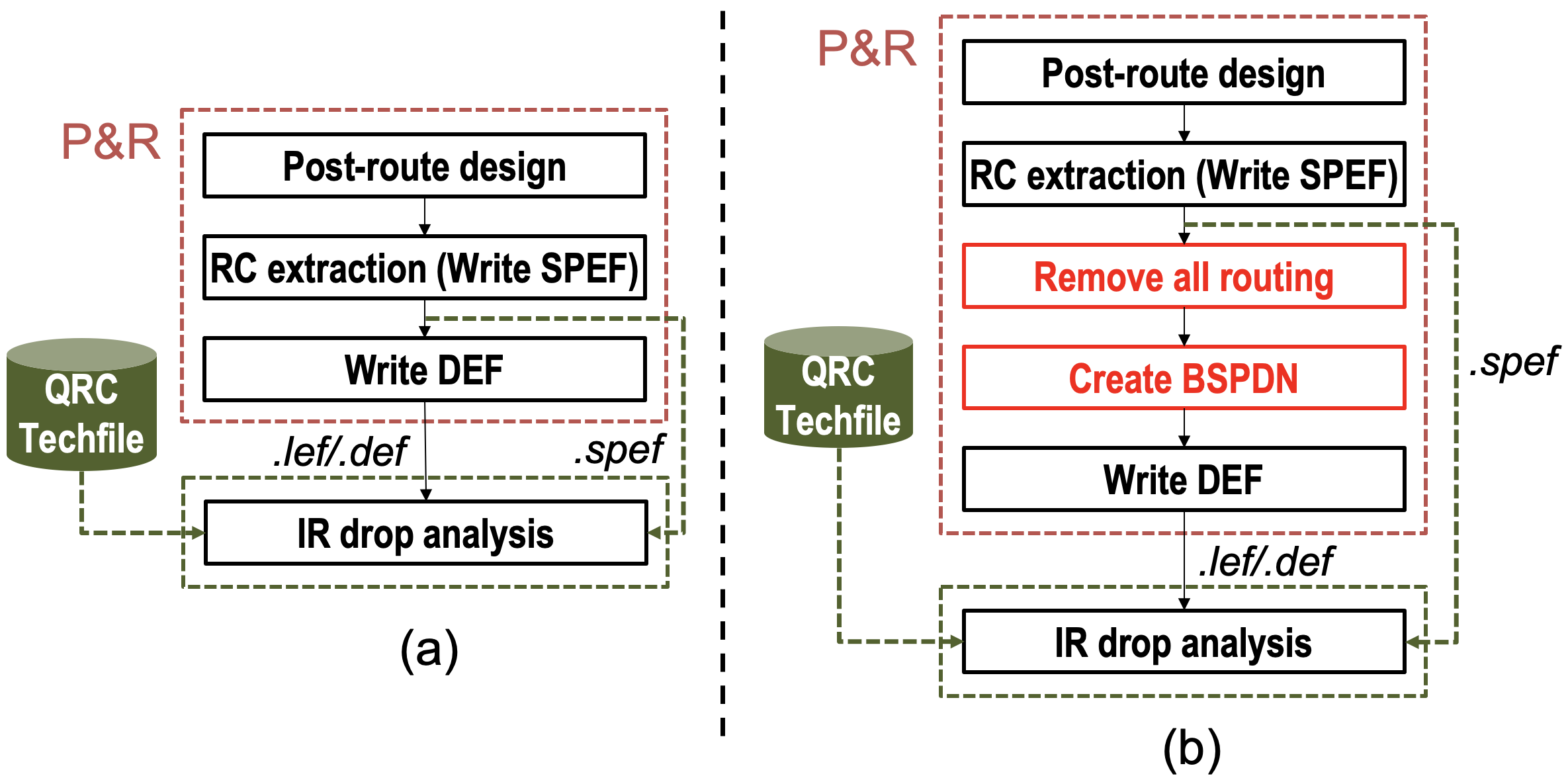
We develop two IR drop analysis flows for FSPDN and BSPDN. Figure 8(a) presents our IR drop analysis flow for FSPDN. After P&R, we generate DEF and SPEF files for routed designs using a commercial P&R tool to perform standalone vectorless dynamic IR drop analysis. Additionally, an interconnect technology file (QRC techfile) is needed for RC extraction as input for the IR drop analysis flow. In contrast, Figure 8(b) depicts our IR drop analysis flow for BSPDN. After P&R, we only create a SPEF file from routed designs. We then remove all routed signals and clocks from the P&R database and construct new power stripes for BSPDN. Since the standalone IR drop analysis tool obtains power stripe information from a DEF file, we generate a DEF file after creating power stripes on the backside. There are two backside metal layers, BM1 and BM2. When creating PDN on backside metal layers, we consider M1 as BM1 and M2 as BM2, respectively. For RC extraction with BSPDN, the QRC techfile must be scaled for backside metals since we assume BM1 and BM2 have the same pitches as M12 and M13. Full details are visible in open-source scripts at [48].
V Enhanced Artificial Designs for PPAC Exploration
The use of specific real designs in DTCO and PPAC exploration can bring risk of biases and incorrect decisions regarding technology configurations (e.g., cell architecture or BEOL stack). To avoid such biases, the PROBE1.0 [13] bases its routability assessment on a mesh-like netlist topology, and PROBE2.0 [6] similarly uses a knight’s tour-based topology. However, these artificial topologies have two main limitations as we bring “PP” aspects of PPAC into the picture. First, they are highly regular and cannot capture a wide range of circuit types. Second, they do not mimic timing and power properties of real netlists, as they target routability assessment without regard to timing path structure.
PROBE3.0 overcomes these limitations by generating artificial but realistic netlists with the Artificial Netlist Generator (ANG) of [16][30], for use in PPAC studies. We use the six topological parameters of ANG (see Table V) to generate and explore circuits with various sizes, interconnect complexity, routed wirelengths and timing. Moreover, we apply machine learning (AutoML) to improve the match of generated artificial netlists to targeted (real) netlists.
| Parameter | Definition |
|---|---|
| () | Number of instances. |
| () | Number of primary inputs/outputs. |
| () | Average net degree. The net degree of a net is the number of terminals of the net. |
| () | Average size of net bounding box. The placed (or routed) layout is divided into a bin grid where each bin contains instances. |
| () | Average depth of timing paths. The depth of a given timing endpoint is the maximum number of stages in any fanin combinational path of that endpoint. is the average of all endpoint depths. |
| () | Ratio of the number of sequential cells to the total number of cells. equals to number of sequential cells over total number of instances. |
V-A Comparison of ANG and Real Designs
In this subsection, we study four real designs from OpenCores [41] and the corresponding artificial netlists generated by ANG [16]. Each design is taken through commercial logic synthesis and P&R tools [44][45] in the PROBE3.0 technology, to obtain a final-routed layout. For AES, JPEG, LDPC and VGA, we respectively use target clock periods of 0.2ns, 0.2ns, 0.6ns and 0.2ns, and utilizations of 0.7, 0.7, 0.2 and 0.7. We then extract the six topological parameters from the routed designs and use these parameters to generate artificial netlists with ANG.
We introduce a Score metric to quantify similarity between artificial and real netlists, as defined in Equation (1).
| (1) |
where:
in target parameter set
of output parameter set
number of parameters ()
In Equation (1), target and output parameters are elements and of the target and output parameter sets. For each parameter, we calculate the discrepancy (ratio) between target and output values. The value is the product of these ratios. Ideally, if output parameters are exactly the same as target parameters, is 1. Larger values of indicate greater discrepancy between ANG-generated netlists and the target netlists.
| Design | Parameters | Score | |||||
| AES | 12318 | 394 | 3.28 | 0.55 | 7.98 | 0.04 | - |
| JPEG | 70031 | 47 | 3.09 | 0.21 | 10.36 | 0.07 | - |
| LDPC | 77379 | 4102 | 2.85 | 1.00 | 12.94 | 0.03 | - |
| VGA | 60921 | 185 | 3.71 | 0.42 | 8.25 | 0.28 | - |
| AES* | 10371 | 394 | 3.28 | 0.79 | 5.19 | 0.13 | 8.53 |
| JPEG* | 63185 | 47 | 3.16 | 0.70 | 6.97 | 0.15 | 12.03 |
| LDPC* | 58699 | 4106 | 3.10 | 0.78 | 6.96 | 0.13 | 14.8 |
| VGA* | 64412 | 188 | 3.32 | 0.26 | 6.39 | 0.25 | 2.8 |
Table VI shows the input parameters, extracted parameters and metric in our comparison of real and artificial designs. The causes of discrepancy are complex, e.g., [16] has steps that heuristically adjust average depths of timing paths and the ratio of sequential cells . Also, performing P&R will change the number of instances , the average net degree , and the routing which determines . Hence, it is difficult to identify the input parameterization of ANG that will yield artificial netlists whose post-route properties match those of (target) real netlists. We use machine learning to address this challenge.
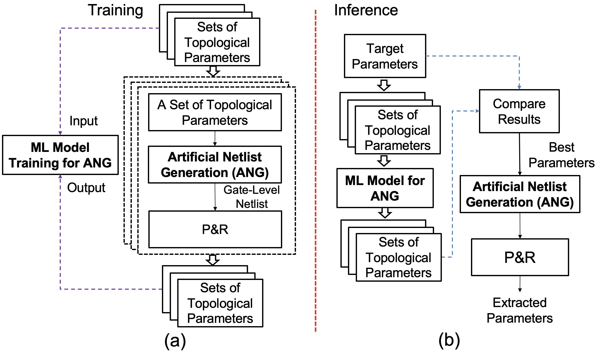
V-B Machine Learning-Based ANG Parameter Tuning
We improve the realism of generated artificial netlists with ML-based parameter tuning for ANG. Figure 9(a) shows the training flow in the parameter tuning. First, to generate training data, we sweep the six ANG input parameters to generate 21,600 combinations of input parameters, as described in Table VII. Second, we use ANG with these input parameter combinations to generate artificial gate-level netlists. Third, we perform P&R with the (21,600) artificial netlists and extract the output parameters. The extracted output parameters are used as output labels for the ML model training. We use the open-source H2O AutoML package [39] (version 3.30.0.6) to predict the output parameters; the StackedEnsemble_AllModels model consistently returns the best model. The model training is a one-time overhead which took 4 hours using an Intel Xeon Gold 6148 2.40GHz server. Executing commercial P&R required just over 7 days in our academic lab setting, and is again a one-time overhead.222The average P&R runtime on our 21,600 ANG netlists is 0.4 hours on an Intel Xeon Gold 6148 2.40GHz server. The data generation used 50 concurrently-running licenses of the P&R tool, with each job running single-threaded. (21,600 0.4 / 50 / 24 7.2 days. With multi-threaded runs, we estimate that data generation would have taken 3 to 4 days.)
Figure 9(b) shows our inference flow. First, we define ranges around the target parameter and sweep the parameters to generate multiple combinations of input parameters as candidates, which are shown in Table VII. Second, we use our trained model to predict the output parameters from each input parameter combination. Note that although there are 12.3M combinations as specified in the rightmost two columns of Table VII, this step requires less than 10 minutes on an Intel Xeon Gold 6148 2.40GHz server.33311 11 21 21 11 21 = 12,326,391. We apply simple filtering based on lower and upper bounds, to avoid parameter values for which ANG does not work properly. Specifically, parameter values are restricted to be within: ; ; ; and . For example, the AES testcase then has 3M input parameter combinations, and predicting output parameters for all of these takes 441 seconds of runtime. Third, we calculate a predicted per each input parameter combination, and then choose the parameter combination with lowest predicted . Finally, we use ANG and the chosen parameter combination to generate an artificial netlist for P&R and PPAC explorations.
Table VIII shows the benefit from ML-based ANG parameter tuning. Columns 2-5 show parameters from real netlists, which we use as target parameters. The trained ML model and the inference flow produce the tuned parameters for ANG shown in Columns 6-9 of the table, and corresponding results are shown in Columns 10-13. The average Score decreases from to 4.89 from the original value of 8.87 for ANG without ML-based parameter tuning (Table VI).
| Parameter | Training Value | Testing Value | |
|---|---|---|---|
| Range | Step | ||
| () | 10000, 20000, 40000, 80000 | 100 | |
| () | 100, 200, 500, 1000, 2000, 4000 | 1 | |
| () | 1.8, 2.0, 2.2, 2.4, 2.6 | 0.02 | |
| () | 0.70, 0.75, 0.80, 0.85, 0.90, 0.95 | 0.02 | |
| () | 6, 8, 10, 12, 14, 16 | 2 | |
| () | 0.2, 0.4, 0.6, 0.8, 1.0 | 0.02 | |
| Parameter | Parameters of Target Netlists | ANG Input Parameters (ML Inference) | Parameters from Artificial Netlists | |||||||||
|---|---|---|---|---|---|---|---|---|---|---|---|---|
| AES | JPEG | LDPC | VGA | AES | JPEG | LDPC | VGA | AES** | JPEG** | LDPC** | VGA** | |
| 12318 | 70031 | 77379 | 60921 | 12718 | 69531 | 76979 | 60421 | 10200 | 64296 | 64796 | 65113 | |
| 394 | 47 | 4102 | 185 | 390 | 42 | 4106 | 199 | 394 | 46 | 4110 | 202 | |
| 3.28 | 3.09 | 2.85 | 3.71 | 3.40 | 3.10 | 3.03 | 3.53 | 3.26 | 3.13 | 3.18 | 3.30 | |
| 0.55 | 0.21 | 1.00 | 0.42 | 0.49 | 0.31 | 1.98 | 0.28 | 0.72 | 0.21 | 0.73 | 0.36 | |
| 7.98 | 10.36 | 12.94 | 8.25 | 13.98 | 18.36 | 20.94 | 12.25 | 8.01 | 9.29 | 11.64 | 8.54 | |
| 0.04 | 0.07 | 0.03 | 0.28 | 0.01 | 0.27 | 0.01 | 0.16 | 0.11 | 0.20 | 0.13 | 0.16 | |
| - | - | - | - | - | - | - | - | 4.39 | 3.59 | 2.77 | 8.81 | |
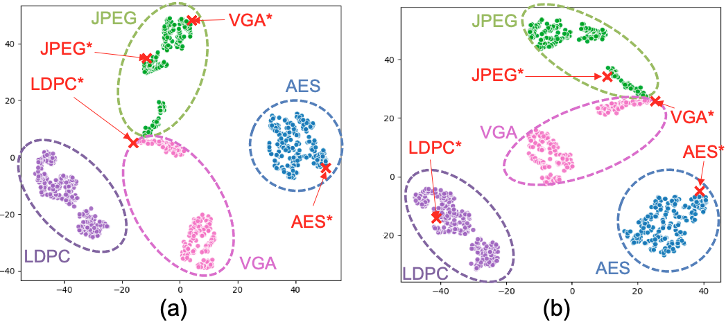
The ML-enabled improvement of realism in ANG netlists can be seen using t-SNE visualization [20] from P&R results. We perform P&R for the four real designs by sweeping initial utilization from 0.6 to 0.8 with a 0.01 step size, and target clock period from 0.15 to 0.25ns with a 0.01ns step size; this results in 21 11 = 231 P&R runs. (For LDPC, we sweep utilization from 0.1 to 0.3 with a 0.01 step size, and clock period from 0.55 to 0.65ns with a 0.01ns step size.) We then perform P&R for artificial netlists with and without our parameter tuning flow, with 0.7 utilization (0.2 for LDPC) and 0.2ns (0.6ns LDPC) target clock period. Figure 10 shows t-SNE visualization444For t-SNE visualization, we collect ten features from P&R results: Number of instances, number of nets, number of primary input/output pins, average fanout, number of sequential cells, wirelength, area, number of design rule violations, worst negative slack, total negative slack, and number of failing endpoints. of the real and artificial designs. The 231 real datapoints per design form well-defined clusters. In Figure 10(a), the datapoints of the artificial AES and JPEG designs are located in the corresponding designs’ clusters. However, the artificial LDPC and VGA designs are not close to the corresponding clusters of real designs. By contrast, Figure 10(b) shows that with our ML-based ANG parameter tuning, datapoints of all four artificial designs are located within the corresponding clusters of real designs. This suggests that the ML-based ANG parameter tuning helps create artificial netlists that better match targeted design parameters – including parameters that are relevant to PPAC exploration.
VI Cell Width-Regularized Placements for More Realistic Routability Assessment
Recall that in the PROBE approach, routability (“AC”) is evaluated using the -threshold () metric [13]. That is, given a placed netlist, routing difficulty is gradually increased by iteratively swapping random pairs of neighboring instances. The cell-swaps progressively “tangle” the placement until it becomes unroutable ( DRCs post-detailed routing). The number of swaps – expressed as a multiple of the instance count – at which routing fails is the metric. Larger implies greater routing capacity or intrinsic routability.
Both PROBE1.0 [13] and PROBE2.0 [6] enable the study of real netlists through the concept of a cell width-regularized placement. In this approach, combinational cells are inflated (by LEF modification) to match the maximum width among all the combinational cells in the cell library. This process, called cell width-regularization, prevents illegal placements (i.e., cell overlaps due to varying widths) from arising due to neighbor-swaps during evaluation. Unfortunately, while cell width-regularization permits real designs to be placed and then tangled by random neighbor-swaps, it also forces low utilizations that harm the realism of the study. (Moreover, high whitespace leads to high values that require more P&R runs to determine.)
We now describe a clustering-based cell width-regularization methodology that generates placements with realistic utilizations, based on real designs. Our experiments in Section VII-D show that clustering-based cell width-regularization obtains the same rank-ordering of design enablements, with less P&R expense, than the previous cell width-regularization approach.
VI-A Clustering-Based Cell Width-Regularization
We propose clustering-based cell width-regularization using bottom-up hypergraph clustering, as detailed in Algorithm 1. In the following, we refer to standard cells of the original netlist as , and (clustered) cells of the clustered netlist as .
Clustered Hypergraph Creation. For a given design, we first obtain a netlist hypergraph using OpenDB [42]. We perform cell width-regularized clustering, where cells (vertices) in the original netlist hypergraph are clustered such that clustered cell width555Given vertex set with cell widths , clustering vertices yields a clustered cell with width + . does not exceed , the maximum cell width in the library. The inputs to cell width-regularized clustering are (i) a hypergraph with vertices , hyperedges and cell widths , (ii) the maximum cell width, , and (iii) a limit on number of clustering iterations, .666In our experiments, we set . However, the cell width-regularized clustering is strongly constrained by , and we observe on our testcases that clustering stops after iterations. The output is a clustered hypergraph (. We use First-Choice (FC) clustering [14] and refer to our clustering method as cell width-regularized clustering with FC, or CWR-FC.
CWR-FC first sorts vertices in increasing order of cell widths (Line 4) and initializes cluster assignments (Line 6). The cluster assignment is the mapping of vertices to clusters ( to ). Clustered cell widths are initialized in Line 7. Next, vertices are traversed in order to perform pairwise clustering; note that only combinational cells are considered for clustering (Line 8). For each vertex that is traversed, we find its neighbors in the hypergraph (Line 11). Each is considered only if it does not violate the limit (Line 14); a cluster score is calculated in Line 15. In the cluster score, is the weight of hyperedge and is the width of vertex . The numerator aims to cluster vertices that are strongly connected (i.e., share many hyperedges) while the denominator promotes clusters of similar widths. If all neighboring vertices violate the threshold width constraint, then no new clusters are formed (Lines 17-19). Otherwise, the vertex with the highest cluster score is selected, and a new cluster is created (Lines 21-24). After all vertices are visited, we construct the clustered hypergraph and proceed with subsequent iterations (Line 28). If no further clustering is feasible, the process terminates (Line 26).
Note that CWR-FC clusters vertices that are adjacent to each other in the hypergraph. However, if all pairings of vertices selected for clustering violate the width constraint, the algorithm can stall (Line 25). To address this issue and improve the uniformity of cluster contents, we perform best-fit bin-packing [11] with bins having capacity (Line 30).777The choice of best-fit is motivated by its simplicity and intuitiveness. Best-fit also enjoys a better approximation ratio compared to first-fit or next-fit alternatives [11]. Finally, the output is the clustered hypergraph .
Clustered Netlist Creation. We convert the clustered hypergraph into Verilog using OpenDB. Then, to run P&R we require a new LEF file that captures the cluster assignments from cell width-regularized clustering. I.e., we require a new netlist over the clusters, .
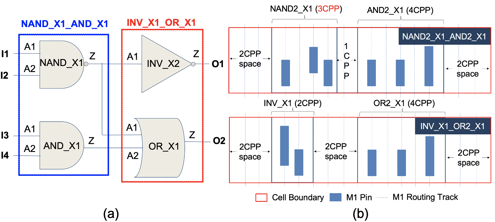
Figure 11(a) provides a schematic view of two clustered cells, NAND_X1_AND_X1 and INV_X1_OR_X1. These correspond to two clusters of original cells: NAND_X1 and AND_X1, and INV_X1 and OR_X1. How the clustered cells are composed from original standard-cell layouts is shown in Figure 11(b). In this case, a non-integer gear ratio between M1P (30nm) and CPP (45nm) forces cells in to be positioned at even CPP sites, to avoid M1 pin misalignment. In the first cluster, NAND_X1 width (3CPP) is an odd number of CPPs, necessitating addition of 1CPP padding between the two cells. In the second cluster, the total cell width is less than , so whitespace is included along with the clustered original cells. We distribute whitespace uniformly, (i) at the sides of and (ii) between consecutive cells in each cluster, as illustrated in Figure 11(b). During this whitespace allocation, we first allocate whitespace at junctions (between consecutive original cells) where no extra padding has been previously allocated.
VI-B Performance of Clustered Cell Width-Regularization
We now document advantages of our proposed clustered cell width-regularization, i.e., more realistic utilization in P&R blocks, and realistic topological and wirelength characteristics of P&R outcomes.
Comparison to Previous Cell Width-Regularization. Figure 12 compares cell width distributions for instances in the clustered netlist and instances in the original netlist. The blue lines show the distribution of cell widths in the original netlist, where smaller cell widths predominate. The red lines indicate that CWR-FC increases the prevalence of cells with larger widths through creation of the merged . The larger amount of actual cell widths in leads to smaller amounts of added whitespace needed to regularize cell widths.
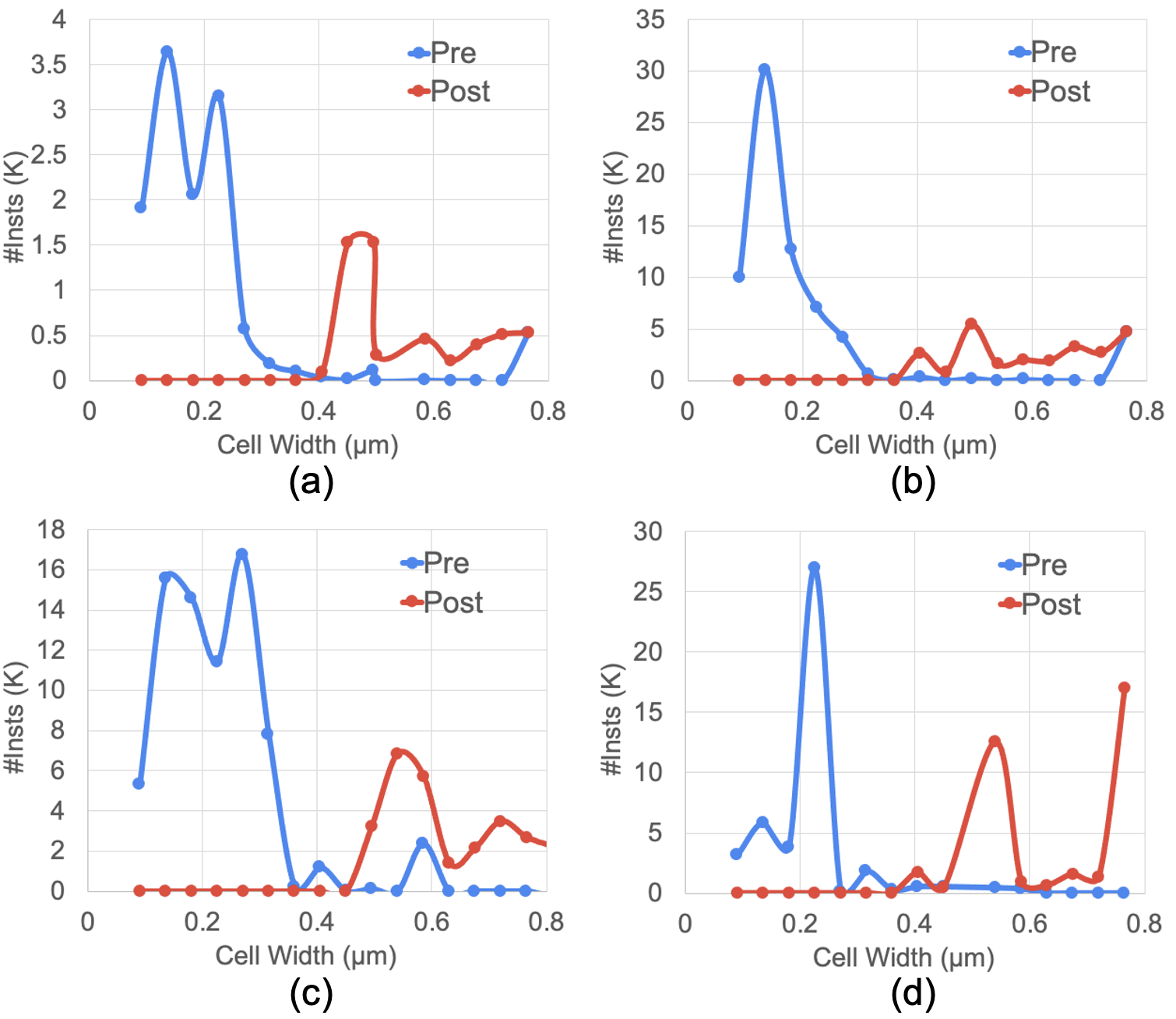
As anticipated, clustered cell width-regularization significantly reduces whitespace in the placed designs. With Lib2 and FSPDN for P&R, placing cell width-regularized instances used in PROBE2.0 at 90% density achieves actual utilizations of 0.21, 0.21 and 0.40 for AES, JPEG and VGA, respectively. For LDPC, placing cell width-regularized instances at 30% density achieves actual utilization of 0.08. By contrast, with clustered cell width-regularization, we achieve actual utilizations of 0.71, 0.74 and 0.71 for AES, JPEG and VGA, respectively. For LDPC, we achieve actual utilization of 0.23. In this way, our new methodology enables evaluation by iterated neighbor-swapping while preserving realistic placement utilizations.
Topological and Wirelength Comparisons to Real Designs. We have confirmed additional similarities between between clustered cell width-regularized netlists and the original real designs. Table IX compares characteristics of our clustering-based cell width-regularized netlists and placements ([C]), versus analogous characteristics of real netlists and placements ([A]). We also implement another plausible clustering methodology, which is to induce clusters from a placement of the original design ([B]). In [B], clusters from the placement are induced by (i) traversing combinational cells left-to-right in each standard cell row, and (ii) clustering maximal contiguous sets of cells without exceeding .
We run P&R using Lib2 and for PDN, maintaining the same core area and utilization. Clustering decreases the number of instances and average fanouts for [B] and [C], relative to [A]. However, wirelengths exhibit no significant changes. The similarities between [A], [B] and [C] suggest that our CWR-FC methodology can preserve netlist properties relevant to P&R outcomes, with more realistic placement utilizations.
| Stage | Design | #Insts | Area () | Util | WL () | Avg. FO |
| [A] | AES | 12318 | 426.254 | 0.83 | 30849 | 2.32 |
| JPEG | 70031 | 2781.981 | 0.73 | 112605 | 2.15 | |
| LDPC | 77379 | 6250.563 | 0.43 | 567630 | 1.85 | |
| VGA | 60921 | 4238.205 | 0.76 | 208845 | 2.71 | |
| [B] | AES | 4275 | 426.254 | 0.83 | 32632 | 1.96 |
| JPEG | 23281 | 2781.981 | 0.73 | 111241 | 1.86 | |
| LDPC | 42383 | 6250.563 | 0.43 | 585923 | 1.43 | |
| VGA | 40084 | 4238.205 | 0.76 | 189612 | 2.14 | |
| [C] | AES | 4661 | 426.254 | 0.83 | 32679 | 2.08 |
| JPEG | 25961 | 2781.981 | 0.73 | 143693 | 1.76 | |
| LDPC | 30636 | 6250.563 | 0.43 | 637417 | 1.29 | |
| VGA | 32768 | 4238.205 | 0.76 | 220915 | 2.02 |
VII Experimental Setup and Results
We have extensively studied the design-technology pathfinding capability of the PROBE3.0 framework using the PROBE3.0 technology. In this section, we report three main experiments. Expts 1 and 2 show PROBE3.0’s capability to assess PPAC trends and tradeoffs, using real and artificial designs respectively. Expt 3 performs assessments of routability and achievable utilization.
In Expts 1 and 2, we analyze four tradeoffs. (i) We present Performance-Power plots that quantify tradeoffs between performance (maximum frequency) and power. (ii) We present Performance-Area plots to quantify the tradeoffs between performance and area. (iii) To address PP aspects, we use the Energy-Delay Product (EDP) [18] as a single metric for power and performance. EDP-Area plots depict tradeoffs between performance/power and area. (iv) We present IR drop-Area plots to demonstrate tradeoffs between IR drop and area. We also compare results obtained using artificial designs with those obtained using real designs. Expt 3 assesses routability and achievable utilization using our clustering-based cell width-regularized placements.
VII-A Experimental Setup
Based on the definition of technology and design parameters in [6], we define ten technology parameters and eight design parameters as the input parameters for the PROBE3.0 framework. Table X describes the definitions of these parameters and the options used in our experiments. Also, we use commercial tools for PDK generation, logic synthesis, P&R, and IR drop analysis. We use open-source tools for GDT-to-GDS translation [38] and SMT solver [49]. Table XI summarizes the tools and versions that we use in our experiments.
| Type | Parameter | Description | Option |
| Technology | The number of fins for devices of standard cells. | 2, 3 | |
| Contacted poly pitch for standard cells in . | 45 | ||
| M0 (horizontal) layer pitch in . | 24 | ||
| M1 (vertical) layer pitch in . | 30 | ||
| M2 (horizontal) layer pitch in . | 24 | ||
| The number of available M0 routing tracks in standard cells. | 4, 5 | ||
| Power/ground pin layer for standard cells. | , | ||
| Cell height of standard cells, expressed as a multiple of . For example, when the cell height in is and is , the cell height () is 5. The cell height value is calculated as for and for . | 5, 6, 7 | ||
| The number of minimum pin openings (access points). | 2 | ||
| Design rules. We define the same grid-based design rules, minimum area rule (DR-MAR), end-of-line spacing rule (DR-EOL) and via spacing rule (DR-VR) as [6]. We use the EUV-tight () design rule set, which includes DR-MAR , DR-EOL and DR-VR . | EUV-Tight | ||
| Design | Metal stack options. We define 14M metal option which contains 14 metal layers (M0 to M13). We define 1.2X, 2.6X, 3.2X and 30X layer pitches based on 24nm as the 1X pitch. | 14M | |
| Power delivery network options. | , , , | ||
| Power tap cell pitch in CPP. | 24, 32, 48, 96, 128 | ||
| Power tap cell insertion scheme. | Column, Staggered | ||
| Commercial P&R tools. | Synopsys IC Compiler II | ||
| Initial placement utilization. | 0.70 to 0.94 with a 0.02 step size | ||
| Designs studied in our experiments. We conduct experiments with four open-source designs from OpenCores [41] and artificial netlists generated by ANG with our ML-based parameter tuning. | AES, JPEG | ||
| Target clock period for logic synthesis and P&R. We define target clock periods that reflect maximum achievable frequencies of the designs. | 0.12 to 0.24ns with a 0.02ns step size |
| Purpose | Tool | Version | Ref. |
|---|---|---|---|
| Format Conversion | GDT-to-GDS translator | 4.0.4 | [38] |
| IR Drop Analysis | Cadence Voltus | 19.1 | [36] |
| Library Characterization | Cadence Liberate | 16.1 | [33] |
| Logic Synthesis | Cadence Genus | 21.1 | [32] |
| Synopsys Design Compiler | R-2020.09 | [44] | |
| LVS | Siemens Calibre | 2017.4_19 | [43] |
| P&R | Synopsys IC Compiler-II | R-2020.09 | [45] |
| PEX | Cadence QRC Extraction | 19.1 | [35] |
| Synopsys StarRC | O-2018.06 | [46] | |
| Siemens Calibre | 2017.4_19 | [43] | |
| SMT solver | Z3 | 4.8.5 | [9][49] |
Criteria for Valid Result. In our experiments, for given , and technology parameters, we perform logic synthesis, P&R and IR drop analysis with multiple sets of parameters including , , and . We use 24, 32, 48, 96 and 128 for , and Column and Staggered for . For , we use values ranging from 0.70 to 0.94 with a step size of 0.02, and for , we use values ranging from 0.12 to 0.24ns with a step size of 0.02ns. Importantly, after the implementation and the analysis steps, we filter out results that are deemed invalid – in that they are likely to fail signoff criteria even with additional human engineering efforts.
To be precise, a “valid” result must satisfy three conditions: (i) the worst negative slack is larger than -50ps; (ii) the number of post-route DRCs is less than 500; and (iii) the 99.7 percentile of the effective instance voltage is greater than 80% of the operating voltage (). To assess (iii), we use a commercial IR drop analysis tool [36] to measure vectorless dynamic IR drop, and calculate the effective instance voltage as per each instance, where is an operating voltage (0.7V) and is the worst voltage drop per instance. We take the 99.7 percentile of effective instance voltage as representative of IR drop for the post-P&R result, as it is within three standard deviations from the mean per the empirical rule [28].
VII-B Expt 1 (PPAC Exploration with Real Designs)
Performance versus Power. We first present PPAC explorations that show tradeoffs between performance and power. (We assume that area is proportional to cost, since chip area is closely related to cost.) In this study, we show results for JPEG with four standard-cell libraries (Lib1-4). Also, we use four PDN structures, , , and , and measure improvements due to scaling boosters relative to the traditional frontside PDN ().
Figure 13(a) gives Performance-Power plots that show tradeoffs between performance and power for JPEG, and improvements from the traditional FSPDN. We calculate the maximum achievable frequency () as where is the target clock period and is the worst negative slack. Also, we add up leakage and dynamic power to obtain the total power. To measure the improvement from , we compare the second-largest value (on the x-axis) attained with each PDN configuration. From the result, we make two main observations. (i) Power consumption with and decreases by 7 to 8%, compared to with the same performance. (ii) Power consumption with is similar to , with the same performance. We observe power reductions from use of scaling boosters, BSPDN and BPR. However, use of BPR without BSPDN does not reduce power consumption.
Performance versus Area. Performance-area tradeoffs for JPEG are shown in Figure 13(b). We make two main observations. (i) Area with , and decreases by up to 8%, 5% and 24%, respectively, as compared to , while maintaining the same level of performance. (ii) We find that use of scaling boosters results in area reductions across all four standard-cell libraries. The area reduction results obtained using the PROBE3.0 framework are consistent with previous industry works [10][22][29][31], which show that use of BSPDN and BPR techniques can result in area reductions of 25% to 30%.
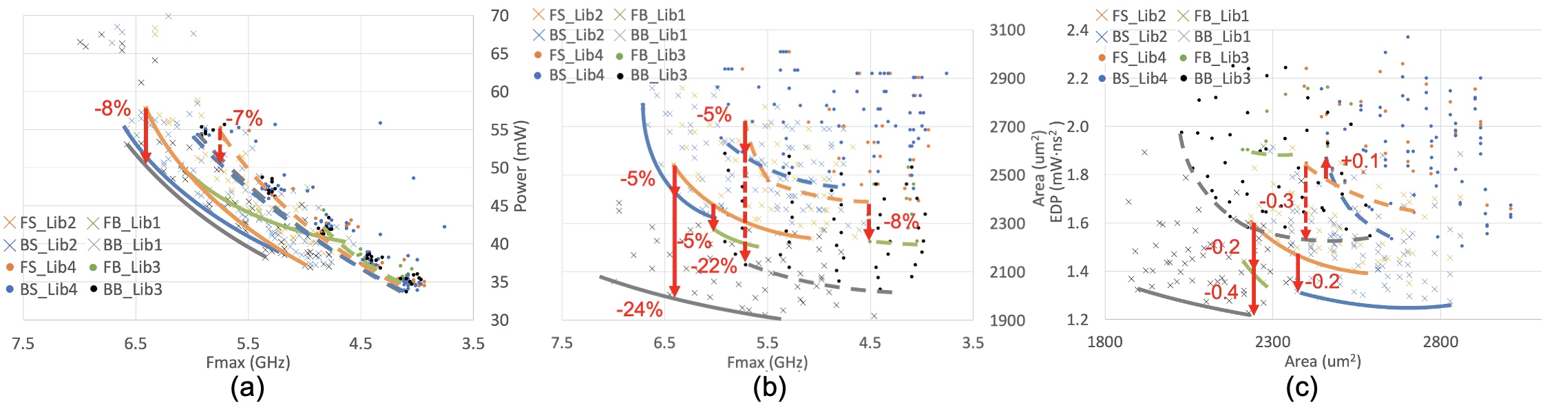
Energy-Delay Product (EDP) versus Area. Given the tradeoffs among PPAC criteria, a simpler metric is useful to comprehend multiple aspects simultaneously. The Energy-Delay Product (EDP) is adopted by, e.g., [18] as a single-value metric that captures both power efficiency and maximum achievable frequency (performance). EDP is calculated as , where denotes power consumption and denotes maximum achievable frequency. Lower EDP means more energy-efficient operations for the chip. Since we address power, performance and area (cost), we draw EDP-Area plots to show PPAC tradeoffs of various PDN structures. We again use four standard-cell libraries (Lib1-4).
From Figure 13(c), we derive four key observations. (i) For (Lib1 and Lib2), EDP with , and decreases by 0.2, 0.2 and 0.4 , respectively, compared to with the same area. (ii) For (Lib3 and Lib4), EDP with decreases by 0.3 , compared to with the same area. (iii) For , EDP with shows no improvements, and EDP with increases by 0.1 , as compared to with the same area. (iv) Use of better optimizes area than other PDN structures with the same EDP.
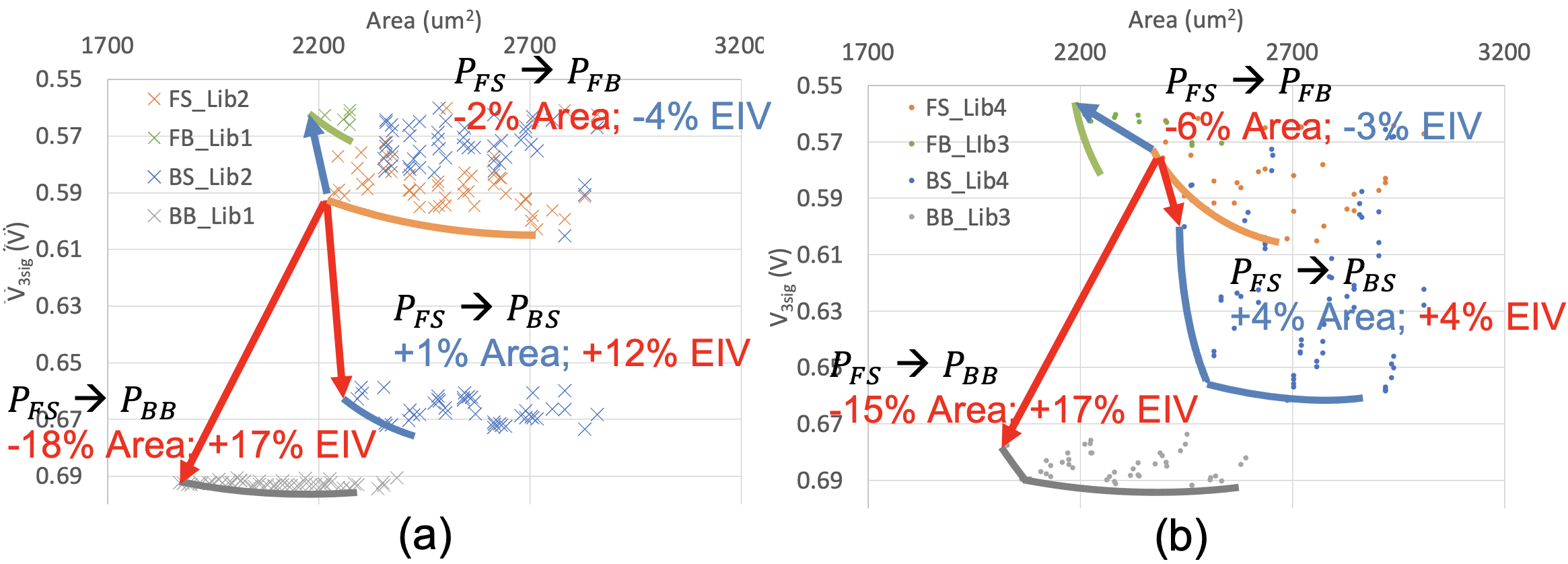
Supply Voltage (IR) Drop versus Area. With recent advanced technologies and designs, denser PDN structures are required due to large resistance seen in tight-pitch BEOL metal layers. The denser PDN structures bring added routability challenges which critically impact area density. In light of this, we measure IR drop and area from valid runs, and plot IR drop-Area tradeoffs in Figure 14. In the plots, we compare the points with the minimum area for each PDN configuration in terms of area and 99.7 percentile (three-sigma) of effective instance voltage (EIV). Note that larger effective instance voltage means better IR drop mitigation. Figures 14(a) and (b) show IR drop-Area tradeoffs for JPEG with (Lib1 and Lib2) and (Lib3 and Lib4), respectively. From the results, we make four main observations. (i) Area with decreases by 2 to 6% compared to , while the effective instance voltage (EIV) increases by 3 to 4%. (ii) Area with increases by 1 to 4% compared to , while EIV decreases by 4 to 12%. (iii) Area with decreases by 15 to 18% compared to , while EIV decreases by 17%. (iv) We observe that there is IR drop mitigation from use of backside PDN, while use of BPR () worsens IR drop. This implies that more power tap cells will need to be inserted to mitigate IR drop. However, the area overhead of power tap cells will degrade the IR drop quality achieved by use of BPR.
VII-C Expt 2 (PPAC Exploration with Artificial Design)
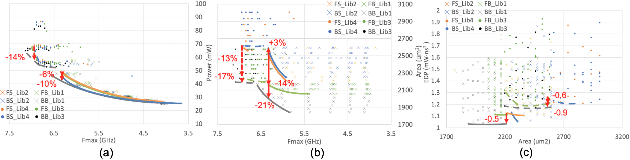
Our second main experiment uses the artificial JPEG design generated by ANG using our ML-based parameter tuning. We conduct the same studies as in Expt 1 and analyze the results.
Performance versus Power. Figure 15(a) shows the tradeoffs between performance and power with the artificial JPEG design. From the result, we make three main observations. (i) Power consumption with and decreases by 6 to 14%, compared to with the same performance. (ii) Power consumption with is similar to with the same performance. (iii) Results with the artificial JPEG show up to 7% differences, but with similar trends, compared to the results obtained with the real JPEG design.
Performance versus Area. Figure 15(b) shows tradeoffs between performance and area with the artificial JPEG design. We make three main observations. (i) Area with and decreases up to 14% and 21% compared to with the same performance. (ii) Area with increases by 0% to 3% compared to with the same performance. This area penalty is caused by power tap cell insertion for . (iii) We observe that the results with the artificial JPEG show up to 9% differences, but with similar trends, compared to the results obtained with the real JPEG design. However, area for shows opposite trends to what we observe with the real design, although the discrepancy is not too large.
Energy-Delay Product (EDP) versus Area. From Figure 15(c), we make three main observations. (i) For (Lib1 and Lib2), EDP with decreases by 0.5 , compared to with the same area. However, EDP with and shows no improvements. (ii) For (Lib3 and Lib4), EDP with and decreases by 0.6 and 0.9 , compared to with the same area. However, EDP with shows no improvements. (iii) We observe that results with the artificial JPEG show similar trends as results obtained with the real JPEG design.
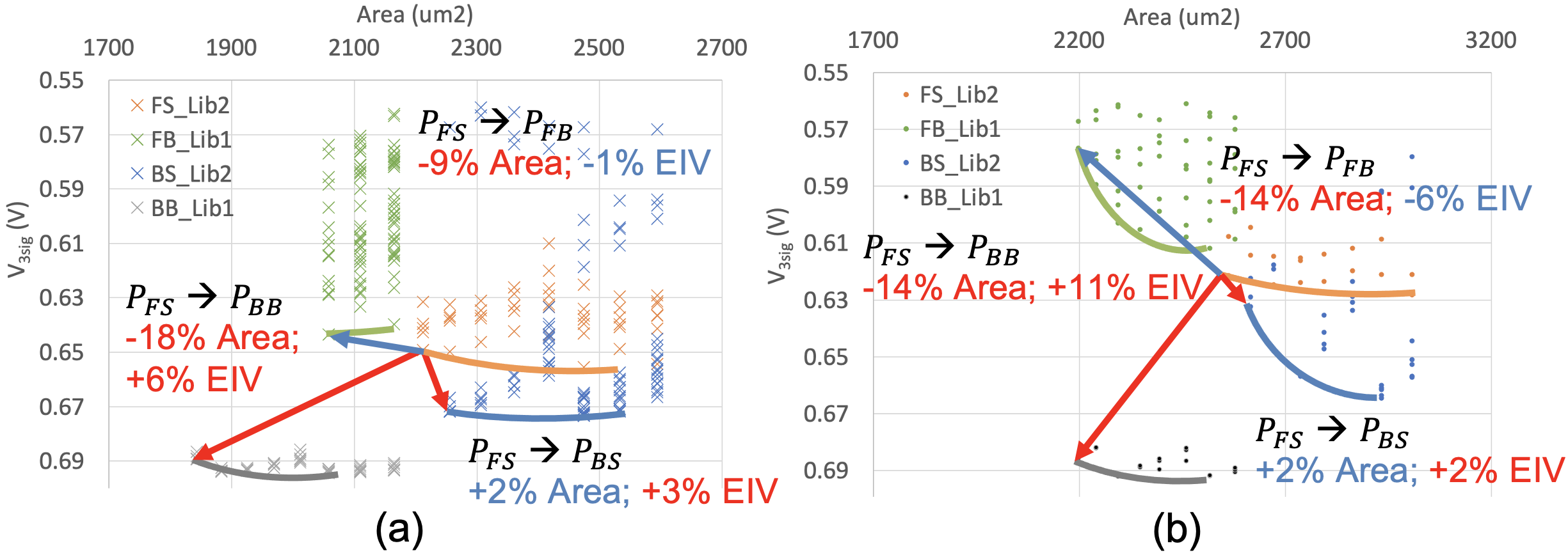
Supply Voltage (IR) Drop versus Area. Figures 16(a) and (b) show tradeoffs between IR drop and area for the artificial JPEG design with (Lib1 and Lib2) and (Lib3 and Lib4), respectively. We make four main observations. (i) Area with decreases by 9 to 14%, compared to , while the effective instance voltage (EIV) increases by 1 to 6%. (ii) Area with increases by 2%, compared to , while EIV decreases by 2 to 3%. (iii) Area with decreases by 14 to 18%, compared to , while EIV decreases by 6 to 11%. (iv) We observe that results with the artificial JPEG show similar trends as results obtained with the real JPEG design, and that discrepancies are reasonably small.
VII-D Expt 3 (Routability Assessment and Achievable Utilization)
Our third main experiment measures using our clustering-based cell width-regularized placements (Section VI), and explores the relationship between and achievable utilization. We note that the previous work of [6] introduced Achievable Utilization as the maximum utilization for which the number of DRCs is less than a predefined threshold of 500 DRCs. Here, we include all three criteria for a valid result (Section VII-A), and define Achievable Utilization as the maximum utilization among all valid runs seen.
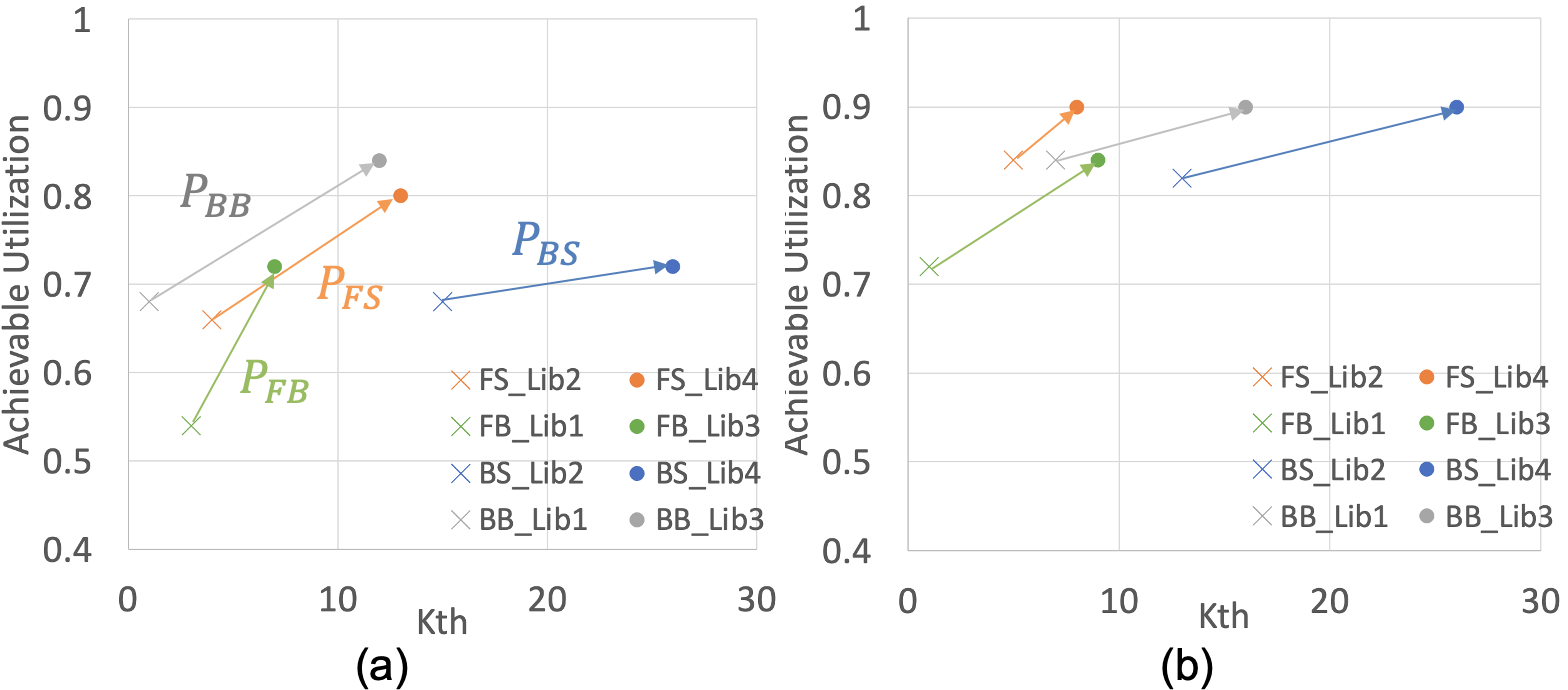
Figure 17 shows experimental results for and achievable utilization. We conduct our experiment with artificial JPEG and four cell width-regularized libraries (Lib1-4). From the plots, we make two observations. (i) We compare the results with / standard-cell libraries (Lib1/2) to those with / standard-cell libraries (Lib3/4). The data show that a larger number of M0 routing tracks brings better routability. (ii) Compared to , and , the plots for are skewed to the right for each design, showing better routability than the other PDN configurations. We observe that the routability improvement of comes from regularly-placed power tap cells: the power tap cell placement eases routing congestion caused by high cell and/or pin density.
Finally, we compare the results obtained with the previous cell width-regularized placements used in the PROBE2.0 work ([A]) and clustering-based cell width-regularized placements obtained using the CWR-FC algorithm of Section VI-A ([C]). We perform routability assessments as summarized in Table XII. We rank-order across the eight combinations of four and two with the JPEG design. The main observation from this comparison is that the ordering of enablements based on is the same for both placements, even as the area utilization of the clustering-based cell width-regularized placements is closer to the initial utilization (0.6). We conclude that our clustering-based cell width-regularized placement methodology successfully provides more realistic placements without disrupting the -based rank-ordering of enablements. Moreover, the generally smaller values seen in the rightmost two columns of Table XII imply fewer P&R trials needed to evaluate the metric.
| Rank | Library | [A] | [C] | ||||
|---|---|---|---|---|---|---|---|
| 1 | 4 | Lib1 | 6 | 0.14 | 3 | 0.50 | |
| 2 | 4 | Lib2 | 9 | 0.14 | 5 | 0.49 | |
| 3 | 4 | Lib1 | 12 | 0.14 | 7 | 0.50 | |
| 4 | 5 | Lib4 | 15 | 0.14 | 8 | 0.50 | |
| 5 | 5 | Lib3 | 16 | 0.14 | 9 | 0.50 | |
| 6 | 4 | Lib2 | 17 | 0.14 | 13 | 0.49 | |
| 7 | 5 | Lib3 | 18 | 0.14 | 16 | 0.50 | |
| 8 | 5 | Lib4 | 23 | 0.14 | 26 | 0.50 | |
VIII Conclusion
We have presented PROBE3.0, a systematic and configurable framework for “full-stack” PPAC exploration and pathfinding in advanced technology nodes. We introduce automated PDK and standard-cell library generation, along with enablement of scaling boosters in a predictive 3nm technology. Our work is permissively open-sourced in GitHub [48], and includes open-sourceable PDKs and EDA tool scripts that incorporate power and performance considerations into the framework.
We employ artificial netlist generation with a machine learning-based parameter tuning to mimic properties of arbitrary real designs. Along with a new CWR-FC clustering-based width-regularized netlist and placement methodology, this enables PPAC exploration of a much wider space of technology, design enablement, and design options. From our experiments, we find that the use of backside power delivery network (BSPDN) and buried power rails (BPR) can lead to up to 8% reduction in power consumption and up to 24% reduction in area using our predictive 3nm technology. These results from PROBE3.0 closely match previous works [10][22][29][31] which estimated 25% to 30% area reduction from use of BSPDN and BPR.
Ongoing and future directions include the following. (i) Improving the software architecture of PROBE3.0 will make it more accessible and flexible for users to pursue their own PPAC explorations. Supporting the addition of user-defined variables can help capture and study variant technology and design assumptions. (ii) To improve robustness of the framework, and its usefulness as a “proxy” in real-world advanced technology development and DTCO, improved device models, parasitic extraction models, signoff corner definitions, relevant design examples, etc. will be beneficial. It will also be necessary to add generation of DRC rule decks for commercial tools. (iii) While our scripts for commercial tools are shared publicly in our GitHub repository, using these tools still requires valid licenses. Incorporation of open-source tools into the PROBE3.0 framework can potentially lead to highly-scaled deployments, shorter turnaround times, and improved utility to a broader audience.
Acknowledgments
We thank Dr. Mustafa Badaroglu at Qualcomm, Dr. Gi-Joon Nam at IBM, Dr. S. C. Song at Google and Prof. Taigon Song at Kyungpook National University for valuable discussions.
References
- [1] A. Agnesina, K. Chang and S. K. Lim, “VLSI Placement Parameter Optimization using Deep Reinforcement Learning”, Proc. ACM/IEEE Intl. Conf. on Computer-Aided Design, 2020, pp. 1-9.
- [2] K. Bhanushali and W. R. Davis, “FreePDK15: An Open-Source Predictive Process Design Kit for 15nm FinFET Technology”, Proc. ACM Intl. Symp. on Physical Design, 2015, pp. 165–170.
- [3] D. Chanemougame, J. Smith, P. Gutwin, B. Byrns and L. Liebmann, “Agile Pathfinding Technology Prototyping: the Hunt for Directional Correctness”, Proc. International Conference on Simulation of Semiconductor Processes and Devices, 2020, pp. 301-305.
- [4] B. Chava, K. A. Shaik, A. Jourdain, S. Guissi, P. Weckx, J. Ryckaert, G. Van Der Plaas, A. Spessot, E. Beyne and A. Mocuta, “Backside Power Delivery as a Scaling Knob for Future Systems”, Proc. SPIE 10962, Design-Process-Technology Co-optimization for Manufacturability XIII 1096205 (2019), pp. 1-6.
- [5] C.-K. Cheng, C.-T. Ho, C. Holtz and B. Lin, “Design and System Technology Co-Optimization Sensitivity Prediction for VLSI Technology Development using Machine Learning”, Proc. ACM/IEEE Intl. Workshop on System-Level Interconnect Prediction, 2021, pp. 1-8.
- [6] C.-K. Cheng, A. B. Kahng, H. Kim, M. Kim, D. Lee, D. Park and M. Woo, “PROBE2.0: A Systematic Framework for Routability Assessment from Technology to Design in Advanced Nodes”, IEEE Trans. on CAD 41(5) (2022), pp. 1495-1508.
- [7] C. Chidambaram, A. B. Kahng, M. Kim, G. Nallapati, S. C. Song and M. Woo, “A Novel Framework for DTCO: Fast and Automatic Routability Assessment with Machine Learning for Sub-3nm Technology Options”, Proc. IEEE Symposium on VLSI Technology, 2021, pp. 1-2.
- [8] L. T. Clark, V. Vashishtha, L. Shifren, A. Gujja, S. Sinha, B. Cline, C. Ramamurthy and G. Yeric, “ASAP7: A 7-nm FinFET Predictive Process Design Kit”, Microelectronics Journal 53 (2016), pp. 105–115.
- [9] L. De Moura and N. Bjørner, “Z3: An Efficient SMT Solver”, Proc. Intl. Conf. on Tools and Algorithms for the Construction and Analysis of Systems, 2008, pp. 337–340.
- [10] M. O. Hossen, B. Chava, G. Van der Plas, E. Beyne and M. S. Bakir, “Power Delivery Network (PDN) Modeling for Backside-PDN Configurations With Buried Power Rails and TSVs”, IEEE Trans. on Electron Devices 67(1) (2020), pp. 11-17.
- [11] D. Johnson, “Near-optimal Bin Packing Algorithms”, Ph.D. Thesis, Massachusetts Institute of Technology, 1973.
- [12] A. B. Kahng, S. Kang, S. Kim and B. Xu, “Enhanced Power Delivery Pathfinding for Emerging 3D Integration Technology”, IEEE Trans. on VLSI 29(4) (2021), pp. 591-604.
- [13] A. Kahng, A. B. Kahng, H. Lee and J. Li, “PROBE: Placement, Routing, Back-End-of-Line Measurement Utility”, IEEE Trans. on CAD 37(7) (2018), pp. 1459-1472.
- [14] G. Karypis, R. Aggarwal, V. Kumar and S. Shekhar, “Multilevel Hypergraph Partitioning: Applications in VLSI Domain”, IEEE Trans. on VLSI 7(1) (1999), pp. 69-79.
- [15] T. Kim, J. Jeong, S. Woo, J. Yang, H. Kim, A. Nam, C. Lee, J. Seo, M. Kim, S. Ryu, Y. Oh and T. Song, “NS3K: A 3-nm Nanosheet FET Standard Cell Library Development and Its Impact”, IEEE Trans. on VLSI 31(2) (2023), pp. 163-176.
- [16] D. Kim, S.-Y. Lee, K. Min and S. Kang, “Construction of Realistic Place-and-Route Benchmarks for Machine Learning Applications”, IEEE Trans. on CAD (2022), doi:10.1109/TCAD.2022.3209530.
- [17] E. D. Kurniawan, H. Yang, C.-C. Lin and Y.-C. Wu, “Effect of Fin Shape of Tapered FinFETs on the Device Performance in 5-nm Node CMOS Technology”, Microelectronics Reliability 83 (2018), pp. 254-259.
- [18] L. Liebmann, D. Chanemougame, P. Churchill, J. Cobb, C.-T. Ho, V. Moroz and J. Smith, “DTCO Acceleration to Fight Scaling Stagnation”, Proc. SPIE 11328, Design-Process-Technology Co-optimization for Manufacturability XIV, 2020, 113280C, pp. 1-15.
- [19] L.-C. Lu, “Physical Design Challenges and Innovations to Meet Power, Speed, and Area Scaling Trend”, Proc. ACM Intl. Symp. on Physical Design, 2017, pp. 63.
- [20] L. Maaten and G. Hinton, “Visualizing Data Using t-SNE”, Journal of Machine Learning Research 9 (2008), pp. 2579-2605.
- [21] D. Prasad, S. S. T. Nibhanupudi, S. Das, O. Zografos, B. Chehab, S. Sarkar, R. Baert, A. Robinson, A. Gupta, A. Spessot, P. Debacker, D. Verkest, J. Kulkarni, B. Cline and S. Sinha, “Buried Power Rails and Back-side Power Grids: Arm® CPU Power Delivery Network Design Beyond 5nm”, Proc. IEEE International Electron Devices Meeting, 2019, pp. 19.1.1-19.1.4.
- [22] J. Ryckaert et al., “Extending the Roadmap Beyond 3nm through System Scaling Boosters: A Case Study on Buried Power Rail and Backside Power Delivery”, Proc. Electron Devices Technology and Manufacturing Conference, 2019, pp. 50-52.
- [23] S. Sadangi, “FreePDK3: A Novel PDK for Physical Verification at the 3nm Node”, M.S. Thesis, Computer Engineering, North Carolina State University, 2021.
- [24] G. Sisto et al., “IR-Drop Analysis of Hybrid Bonded 3D-ICs with Backside Power Delivery and - & n-TSVs”, Proc. IEEE International Interconnect Technology Conference, 2021, pp. 1-3.
- [25] S. C. Song et al., “Unified Technology Optimization Platform using Integrated Analysis (UTOPIA) for Holistic Technology, Design and System Co-Optimization at 7nm Nodes”, Proc. IEEE Symposium on VLSI Circuits, 2016, pp. 1-2.
- [26] H. Su, J. Hu, S. S. Sapatnekar and S. R. Nassif, “Congestion-Driven Codesign of Power and Signal Networks”, Proc. ACM/ESDA/IEEE Design Automation Conference, 2002, pp. 64-69.
- [27] S. S. Teja Nibhanupudi, D. Prasad, S. Das, O. Zografos, A. Robinson, A. Gupta, A. Spessot, P. Debacker, D. Verkest, J. Ryckaert, G. Hellings, J. Myers, B. Cline and J. P. Kulkarni, “A Holistic Evaluation of Buried Power Rails and Back-Side Power for Sub-5nm Technology Nodes”, IEEE Trans. on Electron Devices 69(8) (2022), pp. 4453-4459.
- [28] 68-95-99.7 Rule. https://en.wikipedia.org/wiki/68-95-99.7_rule
- [29] Applied Materials Logic Master Class. https://ir.appliedmaterials.com/static-files/acba6be3-4778-41eb-9183-5c8e52884dea
- [30] Artificial Netlist Generator. https://github.com/daeyeon22/artificial_netlist_generator
- [31] D. O’Laughlin, “Backside Power Delivery and Bold Bets at Intel”, June 2022. https://www.fabricatedknowledge.com/p/backside-power-delivery-and-bold
- [32] Cadence Genus User Guide. http://www.cadence.com
- [33] Cadence Liberate User Guide. http://www.cadence.com
- [34] Cadence PVS User Guide. http://www.cadence.com
- [35] Cadence QRC Extraction User Guide. http://www.cadence.com
- [36] Cadence Voltus User Guide. http://www.cadence.com
- [37] FreePDK3 Predictive Process Design Kit. https://github.com/ncsu-eda/FreePDK3
- [38] GDT to GDS Format Translator. https://sourceforge.net/projects/gds2
- [39] H2O AutoML. https://www.h2o.ai
- [40] IEEE International Roadmap for Devices and Systems (IRDS), 2020 Edition. https://irds.ieee.org/editions/2020
- [41] OpenCores: Open Source IP-Cores. http://www.opencores.org
- [42] OpenDB. https://github.com/The-OpenROAD-Project/OpenDB
- [43] Siemens EDA Calibre User Guide. https://eda.sw.siemens.com/en-US/ic/calibre-design/
- [44] Synopsys Design Compiler User Guide. http://www.synopsys.com
- [45] Synopsys IC Compiler II User Guide. http://www.synopsys.com
- [46] Synopsys StarRC User Guide. http://www.synopsys.com
- [47] Synopsys DTCO Flow: Technology Development. https://www.synopsys.com/silicon/resources/articles/dtco-flow.html
- [48] The PROBE3.0 Framework. https://github.com/ABKGroup/PROBE3.0
- [49] Z3 SMT Solver. https://github.com/Z3Prover/z3