Revealing the two-dimensional electronic structure and anisotropic superconductivity in a natural van der Waals superlattice (PbSe)1.14NbSe2
Abstract
Van der Waals superlattices are important for tailoring the electronic structures and properties of layered materials. Here we report the superconducting properties and electronic structure of a natural van der Waals superlattice (PbSe)1.14NbSe2. Anisotropic superconductivity with a transition temperature = 5.6 0.1 K, which is higher than monolayer NbSe2, is revealed by transport measurements on high-quality samples. Angle-resolved photoemission spectroscopy (ARPES) measurements reveal the two-dimensional electronic structure and a charge transfer of 0.43 electrons per NbSe2 unit cell from the blocking PbSe layer. In addition, polarization-dependent ARPES measurements reveal a significant circular dichroism with opposite contrast at K and K′ valleys, suggesting a significant spin-orbital coupling and distinct orbital angular momentum. Our work suggests natural van der Waals superlattice as an effective pathway for achieving intriguing properties distinct from both the bulk and monolayer samples.
The interlayer coupling plays a critical role in determining the fundamental properties of layered materials Wang et al. (2012); Manzeli et al. (2017), in particular for transition metal dichalcogenides (TMDCs) which exhibit intriguing layer-dependent properties with potential applications in nanoelectronics, optoelectronics, and valleytronics Wang et al. (2012); Xu et al. (2014). Reducing the dimensionality to the two-dimensional (2D) limit leads to distinctive properties from the bulk materials, such as indirect-to-direct bandgap transition Mak et al. (2010); Splendiani et al. (2010), Ising superconductivity with an in-plane upper critical field exceeding the Pauli limit Xi et al. (2016); Lu et al. (2015); Wang et al. (2019); Falson et al. (2020). So far, the dimensionality control has been mostly achieved by mechanical exfoliation of the bulk crystal or growing monolayer film. However, atomically thin films in particular metallic films such as NbSe2 Xi et al. (2016); Wang et al. (2017), WTe2 Cucchi et al. (2019) are often unstable under ambient conditions, and sometimes this can lead to degraded material properties.
Misfit layer compounds (MLCs), natural van der Waals superlattices formed by alternating rock-salt monochalcogenide blocking layer and active TMDC layer along the -axis direction Wiegers and Meerschaut (1992); Wiegers (1996); Dolotko et al. (2020), provide another pathway to tailor the dimensionality and electronic properties of layered materials. By inserting the blocking layer, the interlayer coupling between neighboring active TMDC monolayers is reduced or even removed, while at the same time, the active monolayers are protected by the blocking layers. In this way, 2D properties can be achieved in a bulk van der Waals superlattice with high sample quality and robust sample stability as has been reported in NbS2/Ba3NbS5 Devarakonda et al. (2020). So far, most studies on MLCs have focused on the growth, characterization and transport measurements Devarakonda et al. (2020); Yang et al. (2019); Bai et al. (2018a, 2020, b); Wang et al. (2015), while the effect of the blocking layer on the material properties Leriche et al. (2021); Chikina et al. (2022), as well as the tailored electronic structure of MLC as compared to bulk and monolayer counterparts are only rarely investigated.
In this work, we report the tailored electronic structure of a natural van der Waals superlattice (PbSe)1.14NbSe2, which shows anisotropic superconductivity with a transition temperature = 5.6 K, which is higher than previous reports on the same compound Oosawa et al. (1992); Auriel et al. (1993); Monceau et al. (1994); Auriel et al. (1995); Grosse et al. (2016) as well as monolayer samples Xi et al. (2016); Cao et al. (2015); Ugeda et al. (2016); Xing et al. (2017); Zhao et al. (2019). The 2D electronic structure is revealed by angle-resolved photoemission spectroscopy (ARPES) measurements, and a charge transfer from PbSe to NbSe2 by 0.43 electrons per NbSe2 unit cell is extracted from the size of the Fermi pockets. In addition, polarization-dependent ARPES measurements reveal circular dichroism with opposite contrast for the K and K′ valleys, indicating distinct orbital angular momentum (OAM) and selective excitation of K and K′ valleys. Our work demonstrates natural van der Waals superlattice as an effective pathway for tailoring the electronic structure of layered materials, and for achieving novel properties with potential applications.
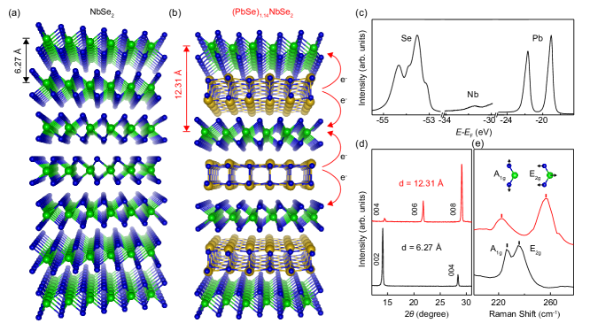
Figure 1(a,b) shows the crystal structures of bulk NbSe2 and (PbSe)1.14NbSe2. High-quality (PbSe)1.14NbSe2 single crystals were grown by chemical vapor transport (CVT) methods Oosawa et al. (1992); Auriel et al. (1993), where the chemical stoichiometry is determined by the ratio of the mismatched -axis periodicities Wiegers (1996). The as-grown samples were characterized by X-ray diffraction (XRD, sensitive to the out-of-plane crystallinity), Laue diffraction (sensitive to in-plane crystal structure) and Raman spectra (sensitive to the lattice vibrations), and a systematic optimization of the growth conditions including precursors, transport agent and temperature gradient is performed to obtain high-quality samples with good reproducibility (see Fig. S1, S2 and Table S1 for more details of sample optimization in Supplemental Material sup ). The optimization of the growth condition can also be applied to other MLCs (see Fig. S3 for more details of growth of other MLCs in Supplemental Material sup ). The high-quality samples pave an important step for transport measurements which reveal a higher superconducting transition temperature, and for electronic structure investigations presented below.
The successful insertion of PbSe blocking layers into NbSe2 is confirmed by characteristic Nb, Se, and Pb peaks in the X-ray photoemission spectroscopy (XPS) spectrum measured on the cleaved surface (Fig. 1(c)). XRD measurements show that the insertion of PbSe blocking layers results in an increase of the interlayer spacing from 6.27 0.01 Å in the bulk NbSe2 (black curve in Fig. 1(d)) to 12.31 0.01 Å in the (PbSe)1.14NbSe2 (red curve in Fig. 1(d)). The increasing interlayer spacing leads to a reduced interlayer coupling and a change of the vibrational modes. A comparison of the Raman spectra in Fig. 1(e) shows that from NbSe2 to (PbSe)1.14NbSe2, the A1g peak shifts from 226.4 cm-1 to 222.4 cm-1 while the E2g peak from 236.4 cm-1 to 256.2 cm-1. The A1g and E2g modes involve Se atoms moving perpendicular and parallel to the Nb plane, and therefore they are particularly sensitive to the interlayer coupling Xi et al. (2015). The redshift of the A1g peak and blueshift of E2g is similar to what is observed from bulk to monolayer MoS2 Lee et al. (2010); Li et al. (2012), indicating weakening of the interlayer coupling in (PbSe)1.14NbSe2 (note that the blueshift of E2g may also attribute to electron doping from PbSe Zhang et al. (2022); Das et al. (2008)).
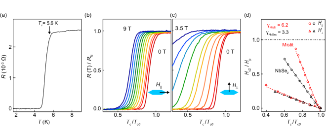
The as-grown (PbSe)1.14NbSe2 exhibits anisotropic superconductivity, which is revealed by transport measurements (Fig. 2). The optimized sample shows a higher transition temperature = 5.6 0.1 K (shown in Fig. 2(a)) compared to previously reported values ranging from 1.1 to 2.5 K Oosawa et al. (1992); Auriel et al. (1993); Monceau et al. (1994); Auriel et al. (1995); Grosse et al. (2016), together with a sharper transition, which possibly originates from the improved sample quality (see Fig. S4 for more details of sample with different quality in Supplemental Material sup ). In addition, the superconductivity shows an anisotropic response to applied magnetic fields - the transition temperature is much less sensitive to the application of in-plane magnetic fields (, Fig. 2(b)) as compared to out-of-plane magnetic fields (, Fig. 2(c)). Figure 2(d) shows the extracted upper critical magnetic fields (normalized by Pauli limit ), and a comparison of (PbSe)1.14NbSe2 (red markers) with bulk NbSe2 (black markers, see Fig. S5 for raw data in Supplemental Material sup ) shows that the superconducting anisotropy is enhanced. To quantify the enhanced anisotropy of superconductivity, the anisotropy factor is defined by , where and are extracted by Lawrence-Doniach model fit Trahms et al. (2018) (shown as dashed lines in Fig. 2(d)). The anisotropy factor is enhanced from for bulk NbSe2 to for (PbSe)1.14NbSe2, which is smaller than the Ising superconductivity in monolayer NbSe2 Xi et al. (2016) with a of 0.9 - 3.7 K Xi et al. (2016); Cao et al. (2015); Ugeda et al. (2016); Xing et al. (2017); Zhao et al. (2019). The enhanced anisotropic is consistent with the increasing interlayer spacing suggested by XRD and Raman measurements in Fig. 1(d,e) which enhances two-dimensional features. We note that similar anisotropy enhancement is also observed in (LaSe)1.14NbSe2 Samuely et al. (2002) and [(SnSe)1+δ]m (NbSe2)1 Trahms et al. (2018), which also confirms that the blocking layer effectively decouples the NbSe2 layer and results in the enhancement of 2D electronic properties.
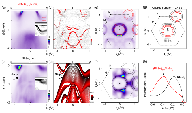
In order to understand the physics underlying the anisotropic superconductivity in (PbSe)1.14NbSe2, ARPES measurements have been performed to reveal the highly 2D electronic structure. Figure 3(a,b) shows a comparison of the experimental electronic structures for (PbSe)1.14NbSe2 and bulk NbSe2. We note that there are two natural cleaving surfaces, with PbSe and NbSe2 terminations respectively, and they show distinctive core levels (see Fig. S6, S7 and Table S2 for more details of two terminations in Supplemental Material sup ). However, the bands near from the Nb orbital Ugeda et al. (2016); Johannes et al. (2006); Calandra et al. (2009), which are the main focus, are observed for both terminations and they show overall similar dispersion. A comparison between the misfit compound and bulk NbSe2 shows that the highly-dispersive 3D bands contributed by Se orbital Johannes et al. (2006) in bulk NbSe2 (pointed by black arrows in Fig. 3(b) and Fig. 3(d)) are missing in (PbSe)1.14NbSe2 (as shown in Fig. 3(a) and Fig. 3(c)), leading to a large energy separation between the bottom of the conduction band and the top of the valence band. The calculated electronic structure of (PbSe)1.14NbSe2 (shown in Fig. 3(c)) agrees qualitatively well with the ARPES results in Fig. 3(a), and they both show distinctive layer-decoupled features that resemble the band structure of monolayer NbSe2 Zhao et al. (2019); Lian et al. (2018); Nakata et al. (2018); Dreher et al. (2021) (see Fig. S8, S9 for more details of first-principles calculation in Supplemental Material sup ). The 2D electronic structure is further supported by the negligible dispersion of (PbSe)1.14NbSe2 (see Fig. S10 for more details of dispersion in Supplemental Material sup ). Therefore, our ARPES measurements together with first-principles calculations show that by expanding the interlayer spacing, the electronic structure of (PbSe)1.14NbSe2 becomes layer-decoupled, as indicated by the disappearance of the highly-dispersive Se bands at the point at different values. Such 2D electronic structure is consistent with the enhanced superconducting anisotropy in response to the applied magnetic fields. We note while PbSe bands are absent near , similar to previous reports in (PbSe)1.16(TiSe2)m Yao et al. (2018), the PbSe blocking layer affects the electronic structure from two aspects. Firstly, the PbSe blocking layer plays an important role in breaking the symmetry of the misfit layer compound, which results in the splitting of the Nb band along the -M direction (see Fig. S11 for more details of D3h symmetry breaking in Supplemental Material sup ). This is also in contrast to the broken inversion symmetry in monolayer NbSe2, where the Nb bands split along -K direction, while they are still degenerate along -M direction Nakata et al. (2018). Secondly, it contributes charges to the neighboring NbSe2 as discussed in details below.
ARPES measurements not only reveal the layer-decoupled electronic structure, but also allow to reveal the charge transfer between PbSe and NbSe2. The carrier concentration can be extracted from the Fermi pockets using the Luttinger theorem Luttinger (1960) and the charge transfer can be directly extracted by the change of the carrier concentration, as has been recently demonstrated in a different misfit layer compound (PbSe)1.16(TiSe2)m Yao et al. (2018). The hole pockets of (PbSe)1.14NbSe2 shown in Fig. 3(e) are clearly smaller than those of bulk NbSe2 (Fig. 3(f)). This suggests a lower hole concentration, indicating electron transfer from the blocking PbSe layers to active NbSe2 layers. Figure 3(g) shows a comparison of the Fermi pockets for bulk NbSe2 (black dotted curves) and (PbSe)1.14NbSe2 (red curves). From the change in the size of the Fermi pockets, a charge transfer of electrons per NbSe2 unit cell from the PbSe layer is revealed (see Fig. S12 for more details in Supplemental Material sup ), which is comparable to the value in (PbSe)1.16(TiSe2)m Yao et al. (2018) and (LaSe)1.14(NbSe2)2 Leriche et al. (2021). Such charge transfer also results in a band shift of the Nb 4 bands by 250 20 meV, as shown by the EDCs in Fig. 3(h). These results demonstrate that the PbSe blocking layers not only provide effective protections for the NbSe2 layers and make NbSe2 layers decoupled, but also inject carriers to NbSe2 layer, thereby tuning the carrier concentration of (PbSe)1.14NbSe2.
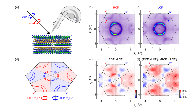
The measured electronic structure confirms that the (PbSe)1.14NbSe2 exhibits 2D electronic properties similar to the monolayer NbSe2, yet with a much larger electron doping due to charge transfer from the PbSe blocking layers. The decoupling of NbSe2 layers suggests that the K and K′ valleys are inequivalent due to the inversion symmetry breaking Xi et al. (2016); Bawden et al. (2016) (see Fig. S13 for more details of inversion symmetry breaking in Supplemental Material sup ), which could result in circular dichroism (CD) Cao et al. (2012) and orbital angular momentum (OAM) Jiang et al. (2015). To search for the OAM and the possible valley pseudospin in (PbSe)1.14NbSe2, we perform polarization dependent ARPES measurements as schematically illustrated in Fig. 4(a) (see Fig. S14 for geometry of CD measurement in Supplemental Material sup ), where the magnetic quantum numbers for right-handed circular polarization (RCP) and left-handed circular polarization (LCP) lights are opposite Park et al. (2012) as shown in Fig. 4(d). Figure 4(b,c) shows the Fermi surface maps measured by RCP and LCP lights, with clear intensity contrast for the K and K′ valleys. The RCP light enhances the intensity of the K valley as indicated by the red arrow in Fig. 4(b), while the LCP light enhances the K′ valley as indicated by the blue arrow in Fig. 4(c). Therefore, the circularly polarized light can selectively couple to these two valleys as schematically summarized in Fig. 4(d), similar to the valleytronics in monolayer MoS2 Cao et al. (2012); Suzuki et al. (2014) (see Table S3 for comparison of CD data to bulk and monolayer in Supplemental Material sup ). Such opposite circular dichroism is more clearly revealed in the differential intensity map shown in Fig. 4(e), which is obtained by subtracting Fig. 4(c) from Fig. 4(b). The circular dichroism is further normalized as Cao et al. (2012) and shown in Fig. 4(f) with an extracted maximum circular dichroism value of 30. The observation of opposite circular dichroism suggests that there is a significant OAM, since the orbital part of the wave function directly couples to the electric field of the incident light Jiang et al. (2015); Park et al. (2012). Considering that there is decoupled interlayer coupling in the MLC, the valley contrasted OAM and the strong spin-orbital coupling (SOC) in NbSe2 implies that there are likely different spin textures in different valleys, similar to the spin texture in monolayer NbSe2 Xi et al. (2016). We note that the correspondence of circular dichroism and spin texture has been revealed on topological insulators Wang et al. (2011); Sánchez-Barriga et al. (2014) and Rashba systems Bian et al. (2012); Bawden et al. (2015); Ishizaka et al. (2011), which also exhibit strong SOC. Here, our results provide the observation of valley-dependent OAM in a MLC system (PbSe)1.14NbSe2, which further demonstrates the tailored 2D behavior in the bulk van der Waals superlattice with potential valleytronics applications.
In summary, we reveal the 2D electronic structure and anisotropic superconductivity in a natural van der Waals superlattice (PbSe)1.14NbSe2. Anisotropic superconductivity with a transition temperature of = 5.6 0.1 K is observed, and opposite circular dichroism at K and K′ valleys shows that circularly polarized light can selectively couple with K and K′ valleys, thereby suggesting (PbSe)1.14NbSe2 as a promising candidate for valleytronics with strong SOC and OAM. The enhanced superconducting anisotropy compared to bulk NbSe2 is attributed to the reduced dimensionality, which is supported by the increasing interlayer spacing supported by XRD and Raman measurements and the 2D electronic structure revealed by ARPES measurements.
Finally, we would like to discuss the physics implied from the misfit layer compound. The enhanced (more Ising-like superconductivity) is related to the breaking of the inversion symmetry in the misfit compound, similar to the case of monolayer NbSe2 Xi et al. (2016). The PbSe blocking layer not only induces charges to the neighboring NbSe2 with a charge transfer of 0.43 electrons, but also it plays a role of protecting the NbSe2. Such protection is a possible reason for why the is higher than monolayer NbSe2, similar to the case of ionic liquid cation intercalated NbSe2 Zhang et al. (2022). Moreover, the incommensurate PbSe blocking layer also leads to breaking of the D3h symmetry, resulting in a splitting of the bands along the -M direction, which is distinguished from monolayer NbSe2. Our work directly reveals the 2D electronic structure underlying the anisotropy superconductivity in MLC, and provides another pathway to tailor the dimensionality and properties of NbSe2 and other layered materials in addition to ionic liquid cation intercalation Zhang et al. (2022), with properties that are distinctive from the bulk samples and monolayer samples.
Acknowledgements.
ACKNOWLEDGMENTS
This work is supported by the National Key RD Program of China (Grant No. 2020YFA0308800, 2021YFA1400100) the National Natural Science Foundation of China (Grant No. 12234011, 92250305, 11725418, 12025405, 11874035, 51788104, 51991343 and 21975140), the National Key RD Program of China (Grant No. 2018YFA0307100 and 2018YFA0305603), and Fundamental Research Funds for the Central Universities (Buctrc202212). H. Z. acknowledges support from the Shuimu Tsinghua Scholar project and the Project funded by China Postdoctoral Science Foundation (Grant No. 2022M721887). This research used resources of the Advanced Light Source, which is a DOE Office of Science User Facility under contract No. DE-AC02-05CH11231; and the Beamline BL09U of the Shanghai Synchrotron Radiation Facility (SSRF).
.1 Conflict of interest
The authors have no conflicts to disclose.
References
- Wang et al. (2012) Q. H. Wang, K. Kalantar-Zadeh, A. Kis, J. N. Coleman, and M. S. Strano, Nat. Nanotechnol. 7, 699 (2012).
- Manzeli et al. (2017) S. Manzeli, D. Ovchinnikov, D. Pasquier, O. V. Yazyev, and A. Kis, Nat. Rev. Mater. 2, 17033 (2017).
- Xu et al. (2014) X. Xu, W. Yao, D. Xiao, and T. F. Heinz, Nat. Phys. 10, 343 (2014).
- Mak et al. (2010) K. F. Mak, C. Lee, J. Hone, J. Shan, and T. F. Heinz, Phys. Rev. Lett. 105, 136805 (2010).
- Splendiani et al. (2010) A. Splendiani, L. Sun, Y. Zhang, T. Li, J. Kim, C.-Y. Chim, G. Galli, and F. Wang, Nano Lett. 10, 1271 (2010).
- Xi et al. (2016) X. Xi, Z. Wang, W. Zhao, J.-H. Park, K. T. Law, H. Berger, L. Forró, J. Shan, and K. F. Mak, Nat. Phys. 12, 139 (2016).
- Lu et al. (2015) J. Lu, O. Zheliuk, I. Leermakers, N. Yuan, U. Heitler, K. Law, and J. Ye, Science 350, 1353 (2015).
- Wang et al. (2019) C. Wang, B. Lian, X. Guo, J. Mao, Z. Zhang, D. Zhang, B.-L. Gu, Y. Xu, and W. Duan, Phys. Rev. Lett. 123, 126402 (2019).
- Falson et al. (2020) J. Falson, Y. Xu, M. Liao, Y. Zang, K. Zhu, C. Wang, Z. Zhang, H. Liu, W. Duan, K. He, et al., Science 367, 1454 (2020).
- Wang et al. (2017) H. Wang, X. Huang, J. Lin, J. Cui, Y. Chen, C. Zhu, F. Liu, Q. Zeng, J. Zhou, P. Yu, et al., Nat. Commun. 8, 394 (2017).
- Cucchi et al. (2019) I. Cucchi, I. Gutiérrez-Lezama, E. Cappelli, S. McKeown Walker, F. Y. Bruno, G. Tenasini, L. Wang, N. Ubrig, C. Barreteau, E. Giannini, et al., Nano Lett. 19, 554 (2019).
- Wiegers and Meerschaut (1992) G. Wiegers and A. Meerschaut, J. Alloys Compd. 178, 351 (1992).
- Wiegers (1996) G. Wiegers, Prog. Solid. State Ch. 24, 1 (1996).
- Dolotko et al. (2020) O. Dolotko, I. Z. Hlova, A. K. Pathak, Y. Mudryk, V. K. Pecharsky, P. Singh, D. D. Johnson, B. W. Boote, J. Li, E. A. Smith, et al., Nat. Commun. 11, 3005 (2020).
- Devarakonda et al. (2020) A. Devarakonda, H. Inoue, S. Fang, C. Ozsoy-Keskinbora, T. Suzuki, M. Kriener, L. Fu, E. Kaxiras, D. C. Bell, and J. G. Checkelsky, Science 370, 231 (2020).
- Yang et al. (2019) X. Yang, J. Ma, B. Lv, H. Hu, T. Sun, M. Li, L. Qiao, S. Wu, Q. Tao, G.-H. Cao, et al., EPL 128, 17004 (2019).
- Bai et al. (2018a) H. Bai, X. Yang, Y. Liu, M. Zhang, M. Wang, Y. Li, J. Ma, Q. Tao, Y. Xie, G.-H. Cao, et al., J. Phys. Condens. Matter 30, 355701 (2018a).
- Bai et al. (2020) H. Bai, L. Qiao, M. Li, J. Ma, X. Yang, Y. Li, Q. Tao, and Z.-A. Xu, Mater. Res. Express 7, 016002 (2020).
- Bai et al. (2018b) W. Bai, P. Li, S. Ju, C. Xiao, H. Shi, S. Wang, S. Qin, Z. Sun, and Y. Xie, J. Phys. Chem. Lett. 9, 6421 (2018b).
- Wang et al. (2015) N. Wang, S. Yuan, R. Cong, X. Lu, F. Meng, C. Shang, and X. Chen, EPL 112, 67007 (2015).
- Leriche et al. (2021) R. T. Leriche, A. Palacio-Morales, M. Campetella, C. Tresca, S. Sasaki, C. Brun, F. Debontridder, P. David, I. Arfaoui, O. Šofranko, et al., Adv. Funct. Mater. 31, 2007706 (2021).
- Chikina et al. (2022) A. Chikina, G. Bhattacharyya, D. Curcio, C. E. Sanders, M. Bianchi, N. Lanatà, M. Watson, C. Cacho, M. Bremholm, and P. Hofmann, Phys. Rev. Mater. 6, L092001 (2022).
- Oosawa et al. (1992) Y. Oosawa, Y. Gotoh, J. Akimoto, T. Tsunoda, M. Sohma, and M. Onoda, Jpn. J. Appl. Phys. 31, L1096 (1992).
- Auriel et al. (1993) C. Auriel, R. Roesky, A. Meerschaut, and J. Rouxel, Mater. Res. Bull. 28, 247 (1993).
- Monceau et al. (1994) P. Monceau, J. Chen, O. Laborde, A. Briggs, C. Auriel, R. Roesky, A. Meerschaut, and J. Rouxel, Physica B Condens. Matter 194, 2361 (1994).
- Auriel et al. (1995) C. Auriel, A. Meerschaut, C. Deudon, G. Wiegers, J. Baas, J. Chen, and P. Monceau, Eur. J. Solid State Inorg. Chem. 32, 947 (1995).
- Grosse et al. (2016) C. Grosse, M. B. Alemayehu, M. Falmbigl, A. Mogilatenko, O. Chiatti, D. C. Johnson, and S. F. Fischer, Sci. Rep. 6, 33457 (2016).
- Cao et al. (2015) Y. Cao, A. Mishchenko, G. L. Yu, E. Khestanova, A. P. Rooney, E. Prestat, A. V. Kretinin, P. Blake, M. B. Shalom, C. Woods, et al., Nano Lett. 15, 4914 (2015).
- Ugeda et al. (2016) M. M. Ugeda, A. J. Bradley, Y. Zhang, S. Onishi, Y. Chen, W. Ruan, C. Ojeda-Aristizabal, H. Ryu, M. T. Edmonds, H.-Z. Tsai, et al., Nat. Phys. 12, 92 (2016).
- Xing et al. (2017) Y. Xing, K. Zhao, P. Shan, F. Zheng, Y. Zhang, H. Fu, Y. Liu, M. Tian, C. Xi, H. Liu, et al., Nano Lett. 17, 6802 (2017).
- Zhao et al. (2019) K. Zhao, H. Lin, X. Xiao, W. Huang, W. Yao, M. Yan, Y. Xing, Q. Zhang, Z.-X. Li, S. Hoshino, et al., Nat. Phys. 15, 904 (2019).
- (32) See the Supplemental Material for additional information about the methods, optimization of sample growth, growth of other MLCs, properties of sample with different quality, superconductivity of pristine bulk NbSe2, observation of different terminations, first-principles calculations of (PbSe)1.14NbSe2, dispersion, D3h symmetry breaking, charge transfer from PbSe to NbSe2, inversion symmetry breaking and more information of circular dichroism data. The Supplemental Material also contains Refs. [33–44].
- Blöchl (1994) P. E. Blöchl, Phys. Rev. B 50, 17953 (1994).
- Perdew et al. (1996) J. P. Perdew, K. Burke, and M. Ernzerhof, Phys. Rev. Lett. 77, 3865 (1996).
- Grimme et al. (2010) S. Grimme, J. Antony, S. Ehrlich, and H. Krieg, J. Chem. Phys. 132, 154104 (2010).
- Kresse and Furthmüller (1996) G. Kresse and J. Furthmüller, Comput. Mater. Sci. 6, 15 (1996).
- Popescu and Zunger (2010) V. Popescu and A. Zunger, Phys. Rev. Lett. 104, 236403 (2010).
- Popescu and Zunger (2012) V. Popescu and A. Zunger, Phys. Rev. B 85, 085201 (2012).
- Wang et al. (2021) V. Wang, N. Xu, J.-C. Liu, G. Tang, and W.-T. Geng, Comput. Phys. Commun. 267, 108033 (2021).
- Lafond et al. (1997) A. Lafond, A. Nader, Y. Moëlo, A. Meerschaut, A. Briggs, S. Perrin, P. Monceau, and J. Rouxel, J. Alloys Compd. 261, 114 (1997).
- Göhler et al. (2018) F. Göhler, G. Mitchson, M. B. Alemayehu, F. Speck, M. Wanke, D. C. Johnson, and T. Seyller, J. Phys. Condens. Matter 30, 055001 (2018).
- Bigi et al. (2021) C. Bigi, F. Mazzola, J. Fujii, I. Vobornik, G. Panaccione, and G. Rossi, Phys. Rev. B 103, 245142 (2021).
- Scholz et al. (2013) M. R. Scholz, J. Sánchez-Barriga, J. Braun, D. Marchenko, A. Varykhalov, M. Lindroos, Y. J. Wang, H. Lin, A. Bansil, J. Minár, et al., Phys. Rev. Lett. 110, 216801 (2013).
- Crepaldi et al. (2014) A. Crepaldi, F. Cilento, M. Zacchigna, M. Zonno, J. C. Johannsen, C. Tournier-Colletta, L. Moreschini, I. Vobornik, F. Bondino, E. Magnano, et al., Phys. Rev. B 89, 125408 (2014).
- Xi et al. (2015) X. Xi, L. Zhao, Z. Wang, H. Berger, L. Forró, J. Shan, and K. F. Mak, Nat. Nanotechnol. 10, 765 (2015).
- Lee et al. (2010) C. Lee, H. Yan, L. E. Brus, T. F. Heinz, J. Hone, and S. Ryu, ACS Nano 4, 2695 (2010).
- Li et al. (2012) H. Li, Q. Zhang, C. C. R. Yap, B. K. Tay, T. H. T. Edwin, A. Olivier, and D. Baillargeat, Adv. Funct. Mater. 22, 1385 (2012).
- Zhang et al. (2022) H. Zhang, A. Rousuli, K. Zhang, L. Luo, C. Guo, X. Cong, Z. Lin, C. Bao, H. Zhang, S. Xu, et al., Nat. Phys. 18, 1425 (2022).
- Das et al. (2008) A. Das, S. Pisana, B. Chakraborty, S. Piscanec, S. K. Saha, U. V. Waghmare, K. S. Novoselov, H. R. Krishnamurthy, A. K. Geim, A. C. Ferrari, et al., Nat. Nanotechnol. 3, 210 (2008).
- Trahms et al. (2018) M. Trahms, C. Grosse, M. B. Alemayehu, O. K. Hite, O. Chiatti, A. Mogilatenko, D. C. Johnson, and S. F. Fischer, Supercond. Sci. Technol. 31, 065006 (2018).
- Samuely et al. (2002) P. Samuely, P. Szabó, J. Kačmarčık, A. Jansen, A. Lafond, A. Meerschaut, and A. Briggs, Physica C 369, 61 (2002).
- Johannes et al. (2006) M. D. Johannes, I. I. Mazin, and C. A. Howells, Phys. Rev. B 73, 205102 (2006).
- Calandra et al. (2009) M. Calandra, I. I. Mazin, and F. Mauri, Phys. Rev. B 80, 241108(R) (2009).
- Lian et al. (2018) C.-S. Lian, C. Si, and W. Duan, Nano Lett. 18, 2924 (2018).
- Nakata et al. (2018) Y. Nakata, K. Sugawara, S. Ichinokura, Y. Okada, T. Hitosugi, T. Koretsune, K. Ueno, S. Hasegawa, T. Takahashi, and T. Sato, NPJ 2D Mater. Appl. 2, 12 (2018).
- Dreher et al. (2021) P. Dreher, W. Wan, A. Chikina, M. Bianchi, H. Guo, R. Harsh, S. Mañas-Valero, E. Coronado, A. J. Martínez-Galera, P. Hofmann, et al., ACS Nano 15, 19430 (2021).
- Yao et al. (2018) Q. Yao, D. W. Shen, C. H. P. Wen, C. Q. Hua, L. Q. Zhang, N. Z. Wang, X. H. Niu, Q. Y. Chen, P. Dudin, Y. H. Lu, et al., Phys. Rev. Lett. 120, 106401 (2018).
- Luttinger (1960) J. Luttinger, Phys. Rev. 119, 1153 (1960).
- Bawden et al. (2016) L. Bawden, S. P. Cooil, F. Mazzola, J. Riley, L. Collins-McIntyre, V. Sunko, K. Hunvik, M. Leandersson, C. Polley, T. Balasubramanian, et al., Nat. Commun. 7, 11711 (2016).
- Cao et al. (2012) T. Cao, G. Wang, W. Han, H. Ye, C. Zhu, J. Shi, Q. Niu, P. Tan, E. Wang, B. Liu, et al., Nat. Commun. 3, 887 (2012).
- Jiang et al. (2015) J. Jiang, F. Tang, X. C. Pan, H. M. Liu, X. H. Niu, Y. X. Wang, D. F. Xu, H. F. Yang, B. P. Xie, F. Q. Song, et al., Phys. Rev. Lett. 115, 166601 (2015).
- Park et al. (2012) S. R. Park, J. Han, C. Kim, Y. Y. Koh, C. Kim, H. Lee, H. J. Choi, J. H. Han, K. D. Lee, N. J. Hur, et al., Phys. Rev. Lett. 108, 046805 (2012).
- Suzuki et al. (2014) R. Suzuki, M. Sakano, Y. Zhang, R. Akashi, D. Morikawa, A. Harasawa, K. Yaji, K. Kuroda, K. Miyamoto, T. Okuda, et al., Nat. Nanotechnol. 9, 611 (2014).
- Wang et al. (2011) Y. H. Wang, D. Hsieh, D. Pilon, L. Fu, D. R. Gardner, Y. S. Lee, and N. Gedik, Phys. Rev. Lett. 107, 207602 (2011).
- Sánchez-Barriga et al. (2014) J. Sánchez-Barriga, A. Varykhalov, J. Braun, S.-Y. Xu, N. Alidoust, O. Kornilov, J. Minár, K. Hummer, G. Springholz, G. Bauer, et al., Phys. Rev. X 4, 011046 (2014).
- Bian et al. (2012) G. Bian, L. Zhang, Y. Liu, T. Miller, and T.-C. Chiang, Phys. Rev. Lett. 108, 186403 (2012).
- Bawden et al. (2015) L. Bawden, J. M. Riley, C. H. Kim, R. Sankar, E. J. Monkman, D. E. Shai, H. I. Wei, E. B. Lochocki, J. W. Wells, W. Meevasana, et al., Sci. Adv. 1, e1500495 (2015).
- Ishizaka et al. (2011) K. Ishizaka, M. Bahramy, H. Murakawa, M. Sakano, T. Shimojima, T. Sonobe, K. Koizumi, S. Shin, H. Miyahara, A. Kimura, et al., Nat. Mater. 10, 521 (2011).