Current-phase relation of a short multi-mode Bi2Se3 topological insulator nanoribbon Josephson junction with ballistic transport modes
Abstract
We used the asymmetric superconducting quantum interference device (SQUID) technique to extract the current phase relation (CPR) of a Josephson junction with a 3D-topological insulator (TI) \ceBi2Se3 nanobelt as the barrier. The obtained CPR shows deviations from the standard sinusoidal CPR with a pronounced forward skewness. At temperatures below 200 mK, the junction skewness values are above the zero temperature limit for short diffusive junctions. Fitting of the extracted CPR shows that most of the supercurrent is carried by ballistic topological surface states (TSSs), with a small contribution of diffusive channels primarily due to the bulk. These findings are instrumental in engineering devices that can fully exploit the properties of the topologically protected surface states of 3D TIs.
1. Introduction
Topological superconductivity and Majorana zero-energy modes have attracted vast interest over the past few years owing to their potential for topologically-protected quantum information processing [1, 2, 3]. Hybrid devices involving a conventional s-wave superconductor (S) in proximity to a semiconducting nanowire with strong spin-orbit coupling [4, 5] or an unconventional metal such as a 3D topological insulator (3D-TI) [6, 7, 8] are expected to provide platforms for emulating and studying this exotic phenomena. One of the standard implementations of such hybrid devices includes S-3DTI-S junctions that exploit the topological surface states for hosting Majorana Bound States (MBSs). Over the past decade, such Josephson junctions based on TI materials have been fabricated and extensively studied experimentally [9, 10, 11, 12, 13, 14, 15, 16, 17, 18, 19, 20, 21, 22, 23, 24, 25, 26, 27, 28, 29, 30]. Here, Majorana physics manifests as peculiar properties of a part of the Andreev bound states (ABSs) carrying the Josephson current across the junction, namely Majorana bound states (MBSs). In an S-TI-S junction with multiple transport modes, MBSs are gapless even for not perfectly transparent S-TI interferences, and under proper conditions, they should show a 4 periodic current phase relation (CPR) coexisting with a 2 periodic CPR due to conventional ABS [7, 31, 32, 8]. The two periodicities should be reflected in the total CPR of the junction, and by probing it one could get access to the unconventional physics of MBSs [9, 10, 11, 12, 13, 14, 15, 16, 17, 18, 19, 20, 21, 22, 23, 24, 25, 27, 28, 29, 30].
The CPR of the junction can be probed using various DC and RF measurement techniques. These include current biased asymmetric DC-SQUIDs [33, 12, 13, 34, 35, 36, 22, 37, 38], and magnetic field pattern measurements of single junctions [9, 39, 40, 36, 41], phase-controlled junctions [19], microwave-induced Shapiro steps [42, 14, 43, 15, 16, 18, 44, 45, 27, 30] and RF-SQUIDs coupled to microwave resonator readouts [46, 47]. However, the critical point to note when looking for a periodic CPR of MBSs is that if the temporal variation of the phase across the junction is slower compared to the inelastic scattering time or the quasi-particle poisoning time, these processes will restore the periodicity of the CPR [7, 48]. As a result, the recent studies aimed at detecting MBSs based on TI-junctions primarily focus on Shapiro step measurements at frequencies larger than any relaxation or poisoning rate [14, 15, 16, 18, 27, 30] or microwave probing of phase-biased Josephson junctions [46]. The missing of odd integer Shapiro steps were reported, pointing toward the possible presence of periodic modes in TI junctions [14, 15, 16, 18, 27, 30, 42, 43, 45].
A significant obstacle in revealing MBSs using Josephson junctions based on 3D-TI like \ceBi2Se3, \ceBi2Te3, and \ceSb2Te3 is the coexistence of bulk states in addition to the topological surface states (TSSs), making the electrical transport analysis cumbersome [6, 49]. Compensation doping has been used to reduce the bulk contribution, however, at the expense of electron mobility [10, 20, 21, 22, 25, 24, 27, 28, 29]. Another approach for reducing the bulk contribution to the electric transport is to increase the surface-to-volume ratio of the 3D TI by growing the material in the shape of nanowires or nanobelts [50, 51, 52]. Previous studies have shown high-quality interfaces between 3D-TI Bi2Se3 nanobelts and Al electrodes. These Josephson junctions show multiple Andreev reflections and large excess currents in the current-voltage characteristics [17, 23]. Here, we further explore the properties of these junctions. Since the results we present here are based on DC measurements, we do not expect to observe any signature of MBS in the Josephson properties [7, 48]. Rather, our study is aimed at characterizing ABS in 3D-TI nanobelt-based junctions.
In this work, we study the CPR of a \ceBi2Se3 nanobelt-based Josephson junction embedded in an asymmetric dc-SQUID. To keep the analysis simple, we focus on junctions in the short limit where the superconducting coherence length is larger than the length of the junction . Here the ABSs dispersion takes a simple form given by , where is the superconducting gap, and correspond to the Andreev level energy and transmission probability of the nth mode, respectively, and is the phase difference across the junction [53]. The corresponding CPR of a short junction can be written as,
| (1) |
where is the temperature, is the corresponding superconducting gap, , , and are the reduced Planck constant, Boltzmann constant, and electron charge, respectively. In the above equation, the sum is taken over all transport modes in the TI junction. In TI nanobelts, spatial confinement along the transversal direction results in the formation of electronic sub-bands and a gap at the Dirac node [23, 27]. This prevents the observation of a perfectly transmissive transport mode. Even though we should not expect a mode with transparency 1, one should still be able to observe the contributions of transport modes with transparency close to one due to the peculiar linear Dirac dispersion in the surface states modes. The demonstration of these high transparency modes is the main objective of this paper.
2. Methods
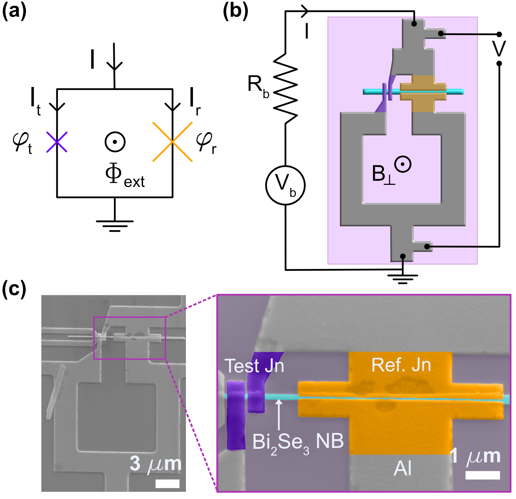
The asymmetric dc-SQUID measurement is a powerful technique to extract the current phase relation (CPR) of Josephson junctions [33, 54, 55, 21, 22]. Here, the test junction with unknown CPR is integrated into a dc-SQUID layout along with a reference junction with known CPR and sufficiently higher critical current , typically 15-20 times larger than the critical current of the test junction , see figure 1.(a). Here and are the phases across the test and reference junctions, respectively. If the inductance of the SQUID loop, , is small enough such that the screening parameter , upon application of an external magnetic flux, , the phase across the test junction is given by , with the superconductive flux quantum [33]. Due to the large asymmetry of the critical currents, the phase across the reference junction remains approximately constant in applied magnetic flux. Therefore the maximum critical current of the SQUID is obtained for at , where the current through the reference junction is maximized, while the phase across the test junction, , varies approximately linearly with [33]. Thus, the CPR of the test junction can be determined by subtracting the constant contribution of the reference junction, , assuming a point-like junction, from the total critical current of the SQUID and going from flux to phase following the relation,
| (2) |
For a tunnel-like reference junction, one gets . However, for our devices, the reference junction is not a conventional tunnel junction. Indeed, nano-processing steps, especially the ones involving heating or etching, tend to alter the properties of TI materials. Therefore we opted to use only a single lithography step to reduce damage to the TI- junctions during device fabrication. In this case, even though the CPR of the reference junction is not known a priori, as long as , one can still extract the CPR of the test junction. However, in this case is not . Earlier experiments have shown that this approach is reliable for extracting the CPR of the test junction [54, 55, 38].
We have realized Josephson junctions using \ceBi2Se3 nanobelts, grown by physical vapor deposition, which are at least 7-8 long to be able to fabricate both the test and reference junction on the same nanobelt [17, 26]. The fabrication process involves the dry transfer of nanobelts to a \ceSiO2/Si substrate followed by electron beam lithography (EBL) and metallization. Following our previous works, before e-beam evaporation of the Pt(3nm)/Al(80-100nm) electrodes, a mild Ar ion milling is performed to remove the native oxide on the nanobelts [11, 17, 23]. SEM images of the SQUID device are shown in figure 1.(c). Here, the length and width of the reference junction are defined by the separation between the two Al electrodes and the dimension of the electrodes along the longitudinal direction of the nanobelt, respectively. In contrast, the width of the test junctions is fixed by the width of the nanobelt (see figure 1).
3. Results and discussion
We will focus on measurements from a single representative SQUID (BSH13 A3S2) formed from a \ceBi2Se3 nanobelt of width 188 nm (from SEM in-lens image) and thickness 48 nm (from AFM image, data not shown). Similar behavior has been observed in other devices (data not shown). The test junction has a length nm, and the corresponding width and length of the reference junction are m and nm, respectively. For the ballistic case ( mean free path 200 nm [50]), the coherence length can be estimated using , with m/s the Fermi velocity of the surface states in \ceBi2Se3, [50, 51] and the induced superconducting gap in the surface state. For a typical eV extracted from single junction devices [17] we obtain m, which is much longer than the length of our junctions, placing them in the short junction limit [53]. The SQUID loop line width is kept at 3 m in most sections of the loop to minimize kinetic inductance contributions, and thus have . From the layout of the SQUID loop, by numerically solving the London-Maxwell equations we determined the effective area m2. This results in a modulation period of approximately T. From the same numerical calculations, we also extract a SQUID loop inductance value pH, of which pH correspond to the geometric inductance, and the remaining pH are the kinetic contribution to loop inductance [56]. Here we used a London penetration depth of nm, typical for 100 nm thick Al films [57]. Unless mentioned, all the measurements were carried out in a dilution refrigerator with a base temperature of 19 mK. The measurement lines are equipped with RC filters at the 4K stage and copper powder filters at the mixing chamber stage to minimize environmental noise/radiation reaching the device.
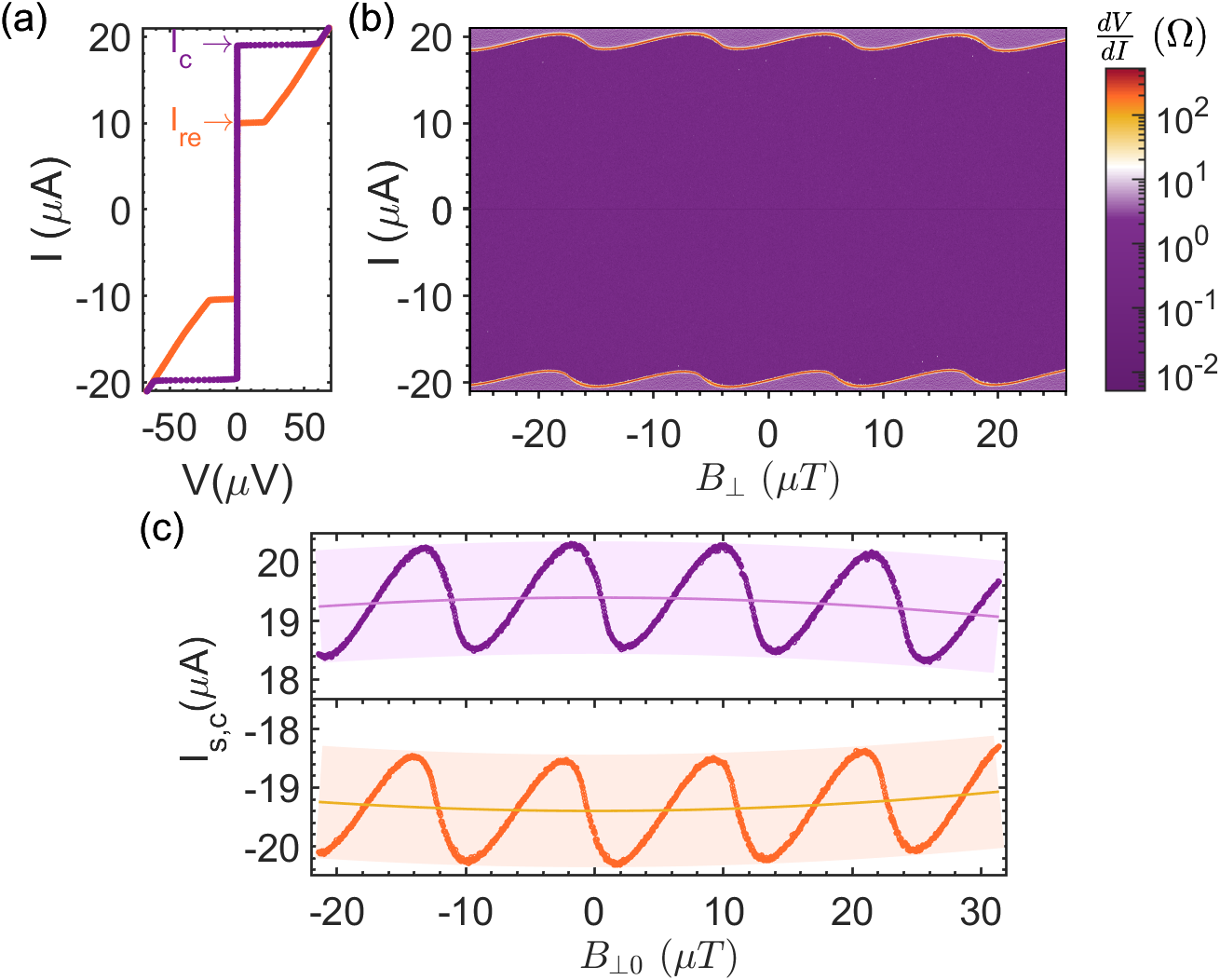
We measured the current-voltage characteristic (IVC) of the SQUID for various externally applied magnetic fields. The IVC of the TI SQUID at zero applied magnetic field is given in figure 2.(a). Here, one can see the typical hysteretic IVC of Al--Al junctions, and we attribute the origin of this hysteresis to heating effects [58, 17]. Now, to get the critical current() of the device, we need to consider the bias sections of the IVC when the junction switches from the superconducting state to the resistive state (in both positive and negative bias directions), which are plotted in purple in figure 2.(a). For the rest of the analysis, we will ignore the sections of IVC where the junction goes back from the resistive state to the superconducting state (plotted in orange in figure 2.(a)), as the switch occurs at the retrapping current (), which is lower than the critical current of the device. Figure 2.(b) shows the variation of the differential resistance of the TI-SQUID with respect to the applied bias current and external magnetic field . Here, one can clearly see the modulations of the critical current from the asymmetric SQUID (bright lines).
Next, we determined the critical current of the SQUID, , from the IVC for every applied magnetic field by setting a threshold voltage of V as the criteria for detecting the switch from the superconducting state to the normal state. The resulting modulation of the positive and negative critical currents are shown as closed symbols in figure 2.(c). On top of the SQUID modulations, we observe a background envelope (solid lines) arising from the magnetic field modulation of the critical current of the reference junction (Fraunhofer pattern). Upon close examination, one could see that the maxima of the Fraunhofer patterns on both positive and negative sides occurred at the field of . This means we have a constant offset in the magnetic field at the device. We see the same magnetic field offset in every measurement that we perform using the setup. To account for this shift, the magnetic field scale in figure 2. (c) is offset to . From the maxima of the Fraunhofer pattern, we get to be 19.4 A. Now, by removing the background due to the reference junction from the total response of the SQUID, one obtains the current modulations of the test junction () as a function of . By converting from magnetic field to flux, using the observed modulation period of T corresponding to one flux quantum , we obtain the current-flux relation (CR) of our test junction for the positive and negative bias currents, as shown in figure 3. (a). From here, we get 880 nA, and the critical current asymmetry in our SQUID device is 22, which is large enough for a proper CPR extraction. Using the simulated value of loop inductance, we can estimate the screening parameter , which is not 1, and we will have to account for finite inductance effects when extracting the CPR.
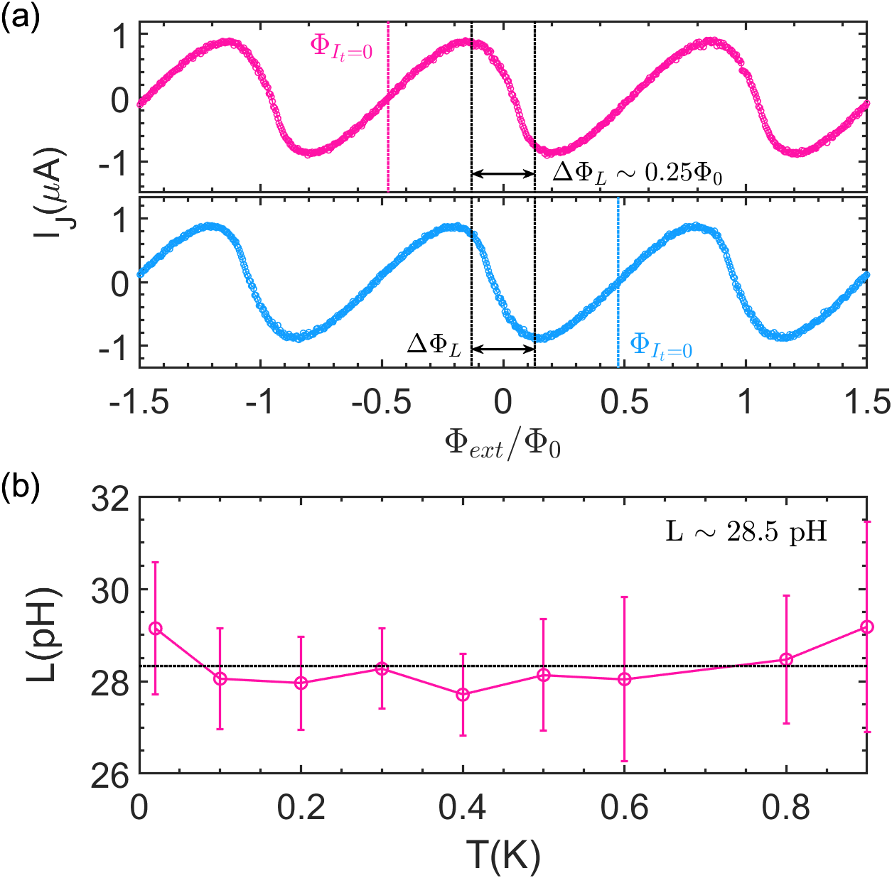
In the following, we will look at the effect of inductance on the extracted CRs and thereby estimate the inductance of the SQUID loop experimentally. From equation 2, one can see that for the negligible inductance case, when the external flux is an integer multiple of , we get . Now, if we assume the CPRs of the test and reference junction have the same functional shape, , the CRs will have the maxima at external flux values which are an integer multiple of . But as seen from figure3.(a), the maxima (in both positive and negative current directions as indicated by the magenta and blue arrows respectively) are offset from integer values. This shift in the CRs is due to the field produced by the circulating current in the SQUID loop, and can be accounted for by modifying the equation for the phase across the test junction as with the total magnetic flux through the SQUID loop [37], assuming the inductance is distributed equally () among the two arms of the SQUID. This shift depends on the direction of the bias current through the SQUID loop, and in our case, the CRs are shifted to the left(right) for positive(negative) bias current. Now to quantify this, for every integer positions, one can define a parameter as the distance between the observed location of the maxima pair corresponding to positive and negative current bias (see the black dotted lines in figure 3.(a)). From the equation for in the finite inductance case, it is straightforward to see that , with the circulating current in the loop when the SQUID critical current is maximized [37]. In our device, by considering four pairs of peaks in the CR (only three are shown for clarity), we obtain corresponding to a loop inductance value of roughly 29 pH. This value is in good agreement with the value that we find from our numerical simulations [56]. In figure 3.(b) we show the extracted SQUID loop inductance for various temperatures up to 900 mK. Here, within the error bars of our data, we do not see a considerable increase in the inductance of the SQUID loop with temperature, confirming that the geometric inductance dominates the loop inductance in the entire temperature range.
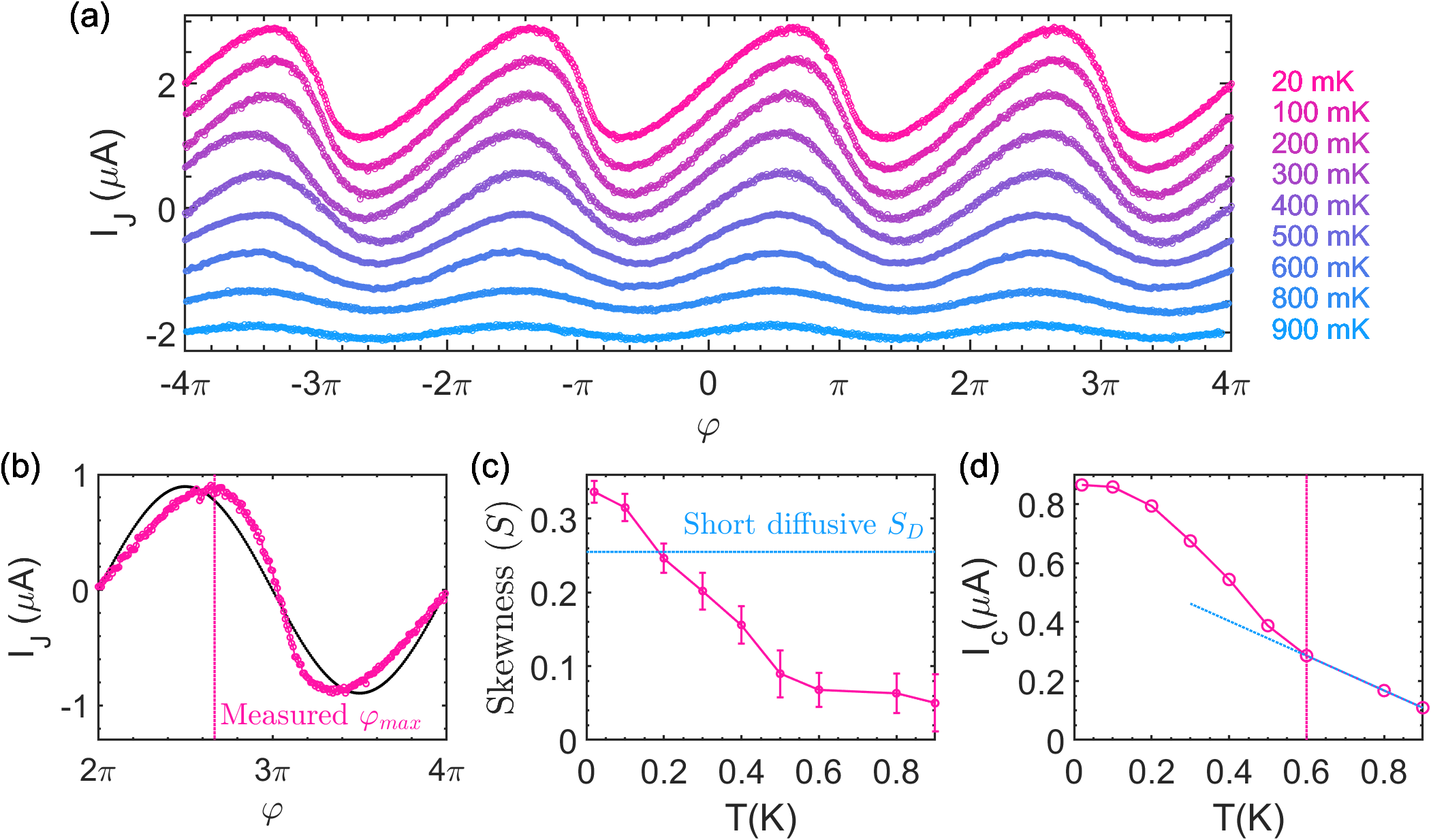
To convert the magnetic flux to the phase drop across the test junction, one should, in principle use equation 2. However, as discussed above, this equation is only valid for zero loop inductance. To account for the finite inductance, we need to subtract from equation 2 the flux shift due to the circulating current. This can be obtained by subtracting the magnetic flux value at which the current of the test junction goes to zero flux (see magenta and blue dotted lines in figure 3.(a)), which accounts for both and the contribution of the circulating current. The resulting CPRs at various temperatures are shown in figure 4.(a). Note that these are not the true CPRs of the test junction. This is because for finite , the flux to phase conversion is not completely linear as in equation 2, and deviations from the linear trend occur around odd multiple integers of (see discussion below) [37]. Also, from here on, we use instead of to indicate the phase across the test junction extracted assuming linear flux to phase conversion and reserve to indicate the actual phase across the test junction.
As seen in figure 4.(a), at low temperatures, the extracted CPRs are forward skewed and evolve into a more sinusoidal CPR at higher temperatures. One commonly used method to quantify the departure of CPRs from a conventional sinusoidal CPR is by defining the skewness, , where corresponds to the phase at which the critical current of the junction is reached [54, 22, 47]. The maximum skewness with is achieved for transmission probability (see equation 1), whereas for one obtains (sinusoidal CPR). We find that at 20 mK, = 0.67, which corresponds to a skewness (see figure 4.(b)). Here, we can rule out any inductance contributions to the position of , since in the limit of a small screening parameter the CPR is affected only in a small phase region around odd integer multiples of (see below). In figure 4.(c) we show the monotonic decrease of the skewness with increasing temperature, asymptotically approaching zero for higher temperatures. We can now compare the skewness parameter to the predictions for different junction regimes. For a short diffusive junction, , with the coherence length, the diffusion constant, and the induced superconducting gap, one expects skewness (see dotted line in figure 4. (c)) [47]. We clearly observe that for temperatures below 200 mK, the transport in our TI junction can not be described by pure diffusive transport. In the limit of Josephson transport coming only from the surface TI channels (TI surface modes) one can estimate the skewness by calculating the CPR using equation 1 and the transmission probabilities following [59], assuming an extreme chemical potential mismatch between the TI channel and the TI covered by the Al electrode,
| (3) |
with quantized electron momentum along longitudinal direction, where is the Fermi wave vector and the quantized transverse momentum given by with and C being the circumference of the nanobelt (). Here we obtain at 20 mK. The fact that the observed skewness parameter is smaller than the one expected for the Josephson current carried exclusively by the surface state suggests that bulk states contribute to the overall current as well. This is supported by the temperature dependence of the critical current (Ic) of the test junction shown in figure 4.(d). The open symbols are the measured data extracted from the CPRs shown in figure 4.(a). As indicated by the dashed lines, around 600 mK we observe a drastic change in the slope of the Ic vs curve that might be due to the presence of two different types of Josephson transport channels with different values as reported in [20, 27]. The Josephson current contribution with higher (same as the Al electrode, K) can be attributed to the ballistic TSSs, while the Josephson current contribution that vanishes fast around 600 mK could be attributed to the diffusive transport modes due to bulk states. This is further supported by the low bulk mobility values we extract from magnetotransport data [51].
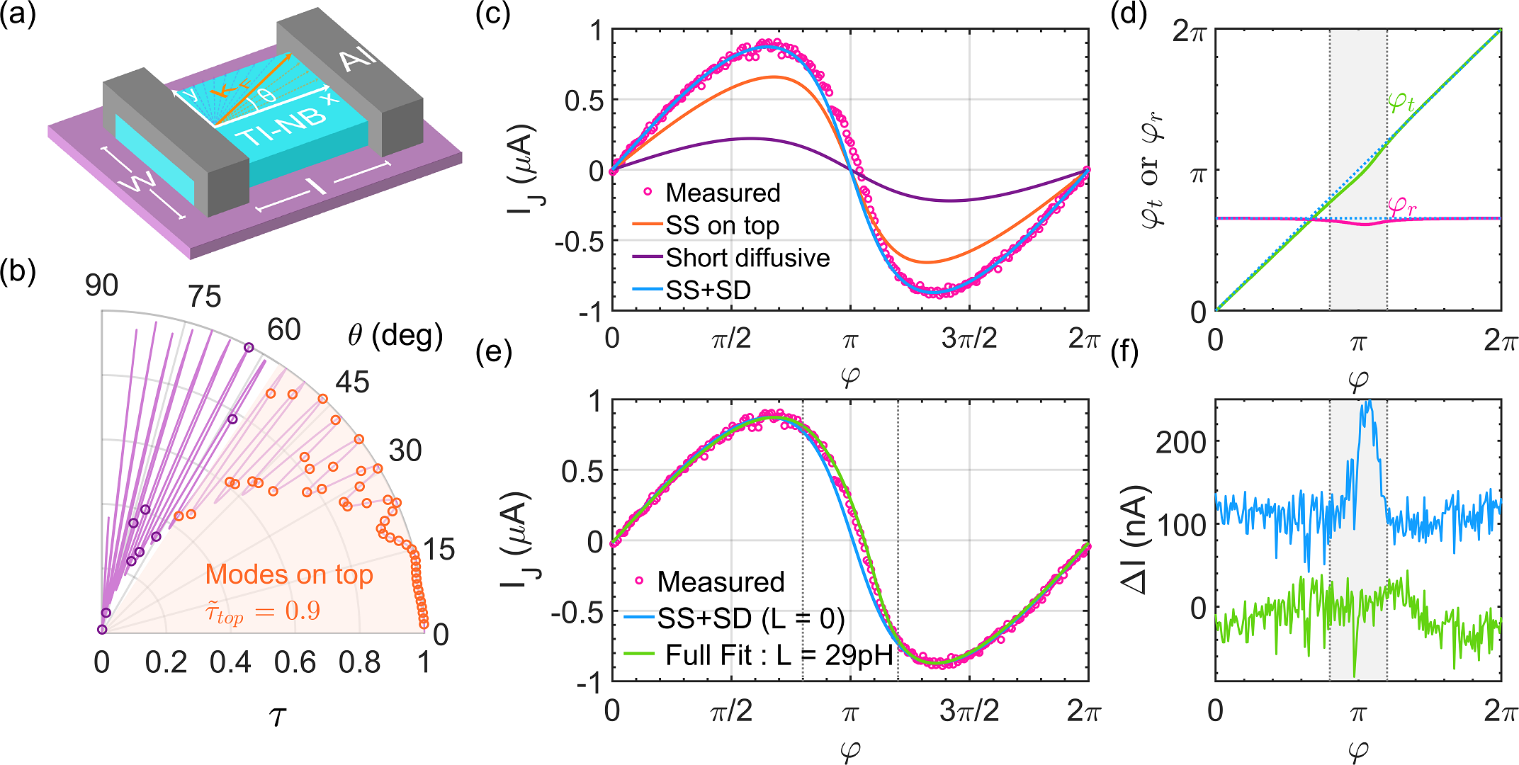
To estimate the individual contributions from the bulk states and surface states to the total Josephson current, we fit the CPR measured at 20 mK (see closed symbols in figure 5.(c)) with a two-band model. For the Josephson current carried by the TSSs we again consider quantized transport modes with transmission probabilities dictated by the geometry of the device, following [59] (see equitation 3). After removing an oxide thickness of 5 nm from the width and thickness, we find for the nanoribbon used in the SQUID, C = 452 nm. Following our previous work, we only consider the modes that travel on the top surface of the TI-belt to be ballistic, as the modes that go around the circumference of the nanobelt suffer from poor mobilities due to the interface with the substrate [51, 23, 52] and/or the paths are longer than the phase coherence length. For the junction geometry, assuming a of 0.55 nm-1 based on magnetotransport measurements performed by us on similar \ceBi2Se3 nanobelts [50, 51, 52], we find that in total there are 39 modes arising from TSSs. Out of these, 29 of them travel on the top surface and should be contributing to the ballistic portion of the supercurrent. In figure 5. (b) we show the polar plot of the transmission probabilities as a function of (continuous) angle (see solid line) using equation 3, displaying Fabry-Pérot-like resonance features in the form of lobes with transmission probabilities very close 1 at certain values related to the geometry of the device [16, 27]. The transmission probabilities of the individual quantized transport modes are shown as open symbols. The orange open symbols correspond to the values of modes that are on the top surface of the junction (up to 48∘). More than half of these modes have values close to 1, resulting in an average value of 0.92 for the modes on the top surface. The modes with above 48∘ (purple open symbols) that go around the circumference are not ballistic as discussed in [23]. So we describe the Josephson current carried by modes that go around the nanobelt and those carried by the bulk states with a diffusive multi-mode model using the Dorokhov distribution of transmission probabilities [60] given by,
| (4) |
where is the normal-state conductance for diffusive modes. Since the value of is unknown, we take it as a fitting parameter in our analysis. Now, the CPR contribution from the diffusive modes is calculated by replacing the sum in equation 1 with an integral in the interval covering the full range of transmission probabilities.
The fitted contributions to the CPR of our junction at 20 mK are shown in figure 5.(c). To fit the CPR, we had to assume a temperature (T mK), which is higher than the bath temperature of 20mK. This discrepancy may have its origins in elevated quasi-particle temperatures or additional current noise typically observed in SNS junctions [33, 61]. The details about noise contributions are beyond the scope of this work and will be described elsewhere. The best fit is obtained when out of the total critical current of 880 nA (see magenta circles corresponding to measured data or blue line corresponding to the sum of ballistic and diffusive parts) of the test junctions, 657 nA are carried by ballistic TSSs on the top of the junction (orange line), and 223 nA are carried by the diffusive transport modes (purple line). The presence of diffusive transport modes with lower skewness will reduce the skewness of the overall CPR of the junction as compared to transport carried entirely by the TSS, in agreement with our experiment.
Finally, we discuss the influence of the finite inductance on the extracted CPR. As one can clearly see in figure 5.(c), the measured CPR does not cross zero at . This is due to the breakdown of the linear mapping between external flux and phase across the test junction around phase values of odd integer multiples of . To resolve this and obtain better flux to phase conversion, one must solve the equation for each value of , including the finite SQUID loop inductance, to get the pairs of phase values and , that maximize the current through the SQUID loop [37]. The variation of and , calculated for a finite inductance value of pH, with respect to is given in figure 5.(d). Here one can see that the curves show deviations around (shaded region) from the expected linear behavior (dashed blue lines) corresponding to zero inductance case. A similar deviation visible in the difference between the measured CPR and the fitted curve is given in figure 5.(f) in the form of a peak around . Now using values, that include inductance effects, we can reproduce the measured CPR relation more accurately and reproduce the zero crossing of the CPR at a phase value slightly larger than as seen in figure 5.(e). This is also reflected in the residual from the fit including the finite inductance of the SQUID loop (see figure 5.(f)). In fact, the peak around disappears, leaving behind mostly the noise from the measurement. Finally, the true CPR of our TI-junction is represented by the blue curve corresponding to the zero inductance fit in figure 5.(c) and (e), and the deviation of the measured CPR from the theorectically expected CPR is simply caused by not fully satisfying the condition . Here, we note that the finite inductance value does not significantly affect the phase position of the maximum of the CPR (see figure 5.(e)), since the position of the maximum and mininmum of the CPR are outside the phase region (in between the dashed gray lines in Fig. 5 (d),(e), and(f)) where deviates from the linear dependence on . Therefore, the various skewness values we extracted earlier are still valid, indicative of the short quasi-ballistic nature of our junction.
4. Conclusions
To conclude, we extracted the CPR of Al-\ceBi2Se3-Al junctions formed out of 3D-TI nanobelts using asymmetric SQUID measurements. We observe a skewed CPR due to the TSSs hosting transport modes with high transmission probabilities. We found that our junctions are, in the short, quasi-ballistic regime, with most supercurrent being carried by ballistic TSSs. However, to fit the extracted CPR, one has to consider both ballistic and diffusive contributions. Therefore, reducing the number of transport modes in these junctions is essential, especially the diffusive bulk contributions, in order to ensure fewer ambiguities in future experiments aimed at detecting MBSs using 3D-TI materials-based devices.
Data availability statement
The main data that support the findings of this study are included
within the article. Additional data are available from the corresponding author upon reasonable request.
Acknowledgement
This work was supported by the European Union’s H2020 under the Marie Curie Actions (No. 766025-QuESTech). This work has been supported by the European Union’s Horizon 2020 Research and Innovation Program (Grant Agreement No. 766714/HiTIMe). K. Niherysh acknowledges the financial support of the “Strengthening of the capacity of doctoral studies at the University of Latvia within the framework of the new doctoral model”, identification no. 8.2.2.0/20/I/006.
ORCID iDs
A. P. Surendran https://orcid.org/0000-0002-0949-4145
D. Montemurro https://orcid.org/0000-0001-8944-0640
G. Kunakova https://orcid.org/0000-0003-0243-2678
X. Palermo https://orcid.org/0000-0001-9997-3053
K. Niherysh https://orcid.org/0000-0002-9861-9957
E. Trabaldo https://orcid.org/0000-0002-0188-6814
D. S. Golubev https://orcid.org/0000-0002-0609-8921
J. Andzane https://orcid.org/0000-0002-9802-6895
D. Erts https://orcid.org/0000-0003-0345-8845
F. Lombardi https://orcid.org/0000-0002-3478-3766
T. Bauch https://orcid.org/0000-0002-8918-4293
References
- A.Yu. Kitaev [2002] A.Yu. Kitaev, Fault-tolerant quantum computation by anyons, Ann. Phys. (N. Y). 303, 2 (2002).
- Nayak et al. [2008] C. Nayak, S. H. Simon, A. Stern, M. Freedman, and S. Das Sarma, Non-Abelian anyons and topological quantum computation, Rev. Mod. Phys. 80, 1083 (2008), arXiv:0707.1889 .
- Sarma et al. [2015] S. D. Sarma, M. Freedman, and C. Nayak, Majorana zero modes and topological quantum computation, npj Quantum Inf. 1, 10.1038/NPJQI.2015.1 (2015), arXiv:1501.02813 .
- Lutchyn et al. [2010] R. M. Lutchyn, J. D. Sau, and S. Das Sarma, Majorana fermions and a topological phase transition in semiconductor-superconductor heterostructures, Phys. Rev. Lett. 105, 1 (2010), arXiv:1002.4033 .
- Mourik et al. [2012] V. Mourik, K. Zuo, S. M. Frolov, S. R. Plissard, E. P. Bakkers, and L. P. Kouwenhoven, Signatures of majorana fermions in hybrid superconductor-semiconductor nanowire devices, Science (80-. ). 336, 1003 (2012), arXiv:1204.2792 .
- Hasan and Kane [2010] M. Z. Hasan and C. L. Kane, Colloquium: Topological insulators, Rev. Mod. Phys. 82, 3045 (2010), arXiv:1002.3895 .
- Fu and Kane [2009] L. Fu and C. L. Kane, Josephson current and noise at a superconductor/quantum-spin-Hall- insulator/superconductor junction, Phys. Rev. B - Condens. Matter Mater. Phys. 79, 1 (2009), arXiv:0804.4469 .
- Tkachov [2019] G. Tkachov, Chiral current-phase relation of topological Josephson junctions: A signature of the 4 -periodic Josephson effect, Phys. Rev. B 100, 1 (2019), arXiv:1903.05131 .
- Williams et al. [2012] J. R. Williams, A. J. Bestwick, P. Gallagher, S. S. Hong, Y. Cui, A. S. Bleich, J. G. Analytis, I. R. Fisher, and D. Goldhaber-Gordon, Unconventional Josephson effect in hybrid superconductor-topological insulator devices, Phys. Rev. Lett. 109, 1 (2012), arXiv:1202.2323 .
- Cho et al. [2013] S. Cho, B. Dellabetta, A. Yang, J. Schneeloch, Z. Xu, T. Valla, G. Gu, M. J. Gilbert, and N. Mason, Symmetry protected Josephson supercurrents in three-dimensional topological insulators, Nat. Commun. 4, 1 (2013).
- Galletti et al. [2014] L. Galletti, S. Charpentier, M. Iavarone, P. Lucignano, D. Massarotti, R. Arpaia, Y. Suzuki, K. Kadowaki, T. Bauch, A. Tagliacozzo, F. Tafuri, and F. Lombardi, Influence of topological edge states on the properties of Al/Bi2Se3/Al hybrid Josephson devices, Phys. Rev. B - Condens. Matter Mater. Phys. 89, 1 (2014), arXiv:1406.0703 .
- Kurter et al. [2015] C. Kurter, A. D. Finck, Y. S. Hor, and D. J. Van Harlingen, Evidence for an anomalous current-phase relation in topological insulator Josephson junctions, Nat. Commun. 6, 2 (2015), arXiv:1307.7764 .
- Sochnikov et al. [2015] I. Sochnikov, L. Maier, C. A. Watson, J. R. Kirtley, C. Gould, G. Tkachov, E. M. Hankiewicz, C. Brüne, H. Buhmann, L. W. Molenkamp, and K. A. Moler, Nonsinusoidal current-phase relationship in josephson junctions from the 3D topological insulator HgTe, Phys. Rev. Lett. 114, 1 (2015).
- Wiedenmann et al. [2016] J. Wiedenmann, E. Bocquillon, R. S. Deacon, S. Hartinger, O. Herrmann, T. M. Klapwijk, L. Maier, C. Ames, C. Brüne, C. Gould, A. Oiwa, K. Ishibashi, S. Tarucha, H. Buhmann, and L. W. Molenkamp, 4-periodic Josephson supercurrent in HgTe-based topological Josephson junctions, Nat. Commun. 7, 1 (2016), arXiv:1503.05591 .
- Bocquillon et al. [2017] E. Bocquillon, R. S. Deacon, J. Wiedenmann, P. Leubner, T. M. Klapwijk, C. Brüne, K. Ishibashi, H. Buhmann, and L. W. Molenkamp, Gapless Andreev bound states in the quantum spin Hall insulator HgTe, Nat. Nanotechnol. 12, 137 (2017), arXiv:1601.08055 .
- Li et al. [2018] C. Li, J. C. de Boer, B. de Ronde, S. V. Ramankutty, E. van Heumen, Y. Huang, A. de Visser, A. A. Golubov, M. S. Golden, and A. Brinkman, 4-periodic Andreev bound states in a Dirac semimetal, Nat. Mater. 17, 875 (2018), arXiv:1707.03154 .
- Kunakova et al. [2019] G. Kunakova, T. Bauch, E. Trabaldo, J. Andzane, D. Erts, and F. Lombardi, High transparency Bi2Se3 topological insulator nanoribbon Josephson junctions with low resistive noise properties, Appl. Phys. Lett. 115, 10.1063/1.5123554 (2019), arXiv:1910.00280 .
- Le Calvez et al. [2019] K. Le Calvez, L. Veyrat, F. Gay, P. Plaindoux, C. B. Winkelmann, H. Courtois, and B. Sacépé, Joule overheating poisons the fractional ac Josephson effect in topological Josephson junctions, Communications Physics 2, 1 (2019), arXiv:1803.07674 .
- Ren et al. [2019] H. Ren, F. Pientka, S. Hart, A. T. Pierce, M. Kosowsky, L. Lunczer, R. Schlereth, B. Scharf, E. M. Hankiewicz, L. W. Molenkamp, B. I. Halperin, and A. Yacoby, Topological superconductivity in a phase-controlled Josephson junction, Nature 569, 93 (2019), arXiv:1809.03076 .
- Schüffelgen et al. [2019] P. Schüffelgen, D. Rosenbach, C. Li, T. W. Schmitt, M. Schleenvoigt, A. R. Jalil, S. Schmitt, J. Kölzer, M. Wang, B. Bennemann, U. Parlak, L. Kibkalo, S. Trellenkamp, T. Grap, D. Meertens, M. Luysberg, G. Mussler, E. Berenschot, N. Tas, A. A. Golubov, A. Brinkman, T. Schäpers, and D. Grützmacher, Selective area growth and stencil lithography for in situ fabricated quantum devices, Nat. Nanotechnol. 14, 825 (2019).
- Kayyalha et al. [2019] M. Kayyalha, M. Kargarian, A. Kazakov, I. Miotkowski, V. M. Galitski, V. M. Yakovenko, L. P. Rokhinson, and Y. P. Chen, Anomalous Low-Temperature Enhancement of Supercurrent in Topological-Insulator Nanoribbon Josephson Junctions: Evidence for Low-Energy Andreev Bound States, Phys. Rev. Lett. 122, 47003 (2019), arXiv:1712.02748 .
- Kayyalha et al. [2020] M. Kayyalha, A. Kazakov, I. Miotkowski, S. Khlebnikov, L. P. Rokhinson, and Y. P. Chen, Highly skewed current–phase relation in superconductor–topological insulator–superconductor Josephson junctions, npj Quantum Materials 5, 1 (2020), arXiv:1812.00499 .
- Kunakova et al. [2020] G. Kunakova, A. P. Surendran, D. Montemurro, M. Salvato, D. Golubev, J. Andzane, D. Erts, T. Bauch, and F. Lombardi, Topological insulator nanoribbon Josephson junctions: Evidence for size effects in transport properties, J. Appl. Phys. 128, 10.1063/5.0022126 (2020), arXiv:2011.04787 .
- De Ronde et al. [2020] B. De Ronde, C. Li, Y. Huang, and A. Brinkman, Induced topological superconductivity in a BiSbTeSe2-based Josephson junction, Nanomaterials 10, 1 (2020).
- Stolyarov et al. [2020] V. S. Stolyarov, D. S. Yakovlev, S. N. Kozlov, O. V. Skryabina, D. S. Lvov, A. I. Gumarov, O. V. Emelyanova, P. S. Dzhumaev, I. V. Shchetinin, R. A. Hovhannisyan, S. V. Egorov, A. M. Kokotin, W. V. Pogosov, V. V. Ryazanov, M. Y. Kupriyanov, A. A. Golubov, and D. Roditchev, Josephson current mediated by ballistic topological states in Bi2Te2.3Se0.7 single nanocrystals, Commun. Mater. 1, 1 (2020).
- Kim et al. [2020] N. H. Kim, H. S. Kim, Y. Hou, D. Yu, and Y. J. Doh, Superconducting quantum interference devices made of Sb-doped Bi2Se3 topological insulator nanoribbons, Curr. Appl. Phys. 20, 680 (2020).
- Rosenbach et al. [2021] D. Rosenbach, T. W. Schmitt, P. Schüffelgen, M. P. Stehno, C. Li, M. Schleenvoigt, A. R. Jalil, G. Mussler, E. Neumann, S. Trellenkamp, A. A. Golubov, A. Brinkman, D. Grützmacher, and T. Schäpers, Reappearance of first Shapiro step in narrow topological Josephson junctions, Sci. Adv. 7, 10.1126/sciadv.abf1854 (2021).
- Bai et al. [2022] M. Bai, X. K. Wei, J. Feng, M. Luysberg, A. Bliesener, G. Lippertz, A. Uday, A. A. Taskin, J. Mayer, and Y. Ando, Proximity-induced superconductivity in (Bi1-xSbx)2Te3 topological-insulator nanowires, Commun. Mater. 3, 1 (2022).
- Schmitt et al. [2022] T. W. Schmitt, M. R. Connolly, M. Schleenvoigt, C. Liu, O. Kennedy, J. M. Chávez-Garcia, A. R. Jalil, B. Bennemann, S. Trellenkamp, F. Lentz, E. Neumann, T. Lindström, S. E. De Graaf, E. Berenschot, N. Tas, G. Mussler, K. D. Petersson, D. Grützmacher, and P. Schüffelgen, Integration of Topological Insulator Josephson Junctions in Superconducting Qubit Circuits, Nano Lett. 22, 2595 (2022).
- Fischer et al. [2022] R. Fischer, J. Picó-Cortés, W. Himmler, G. Platero, M. Grifoni, D. A. Kozlov, N. N. Mikhailov, S. A. Dvoretsky, C. Strunk, and D. Weiss, 4P -Periodic Supercurrent Tuned By an Axial Magnetic Flux in Topological Insulator Nanowires, Phys. Rev. Res. 4, 1 (2022).
- Cook et al. [2012] A. M. Cook, M. M. Vazifeh, and M. Franz, Stability of Majorana fermions in proximity-coupled topological insulator nanowires, Phys. Rev. B - Condens. Matter Mater. Phys. 86, 1 (2012), arXiv:1206.3829 .
- Snelder et al. [2013] M. Snelder, M. Veldhorst, A. A. Golubov, and A. Brinkman, Andreev bound states and current-phase relations in three-dimensional topological insulators, Phys. Rev. B - Condens. Matter Mater. Phys. 87, 1 (2013), arXiv:1302.4206 .
- Della Rocca et al. [2007] M. L. Della Rocca, M. Chauvin, B. Huard, H. Pothier, D. Esteve, and C. Urbina, Measurement of the current-phase relation of superconducting atomic contacts, Phys. Rev. Lett. 99, 1 (2007), arXiv:0708.0515 .
- Spanton et al. [2017] E. M. Spanton, M. Deng, S. Vaitiekenas, P. Krogstrup, J. Nygård, C. M. Marcus, and K. A. Moler, Current-phase relations of few-mode InAs nanowire Josephson junctions, Nat. Phys. 13, 1177 (2017), arXiv:1701.01188 .
- Murani et al. [2017] A. Murani, A. Kasumov, S. Sengupta, Y. A. Kasumov, V. T. Volkov, I. I. Khodos, F. Brisset, R. Delagrange, A. Chepelianskii, R. Deblock, H. Bouchiat, and S. Guéron, Ballistic edge states in Bismuth nanowires revealed by SQUID interferometry, Nat. Commun. 8, 1 (2017), arXiv:1609.04848 .
- Assouline et al. [2019] A. Assouline, C. Feuillet-Palma, N. Bergeal, T. Zhang, A. Mottaghizadeh, A. Zimmers, E. Lhuillier, M. Eddrie, P. Atkinson, M. Aprili, and H. Aubin, Spin-Orbit induced phase-shift in Bi 2 Se 3 Josephson junctions, Nat. Commun. 10, 10.1038/s41467-018-08022-y (2019), arXiv:1806.01406 .
- Nichele et al. [2020] F. Nichele, E. Portolés, A. Fornieri, A. M. Whiticar, A. C. Drachmann, S. Gronin, T. Wang, G. C. Gardner, C. Thomas, A. T. Hatke, M. J. Manfra, and C. M. Marcus, Relating Andreev Bound States and Supercurrents in Hybrid Josephson Junctions, Phys. Rev. Lett. 124, 1 (2020), arXiv:1912.08893 .
- Mayer et al. [2020] W. Mayer, M. C. Dartiailh, J. Yuan, K. S. Wickramasinghe, E. Rossi, and J. Shabani, Gate controlled anomalous phase shift in Al/InAs Josephson junctions, Nat. Commun. 11, 10.1038/s41467-019-14094-1 (2020), arXiv:1905.12670 .
- Ghatak et al. [2018] S. Ghatak, O. Breunig, F. Yang, Z. Wang, A. A. Taskin, and Y. Ando, Anomalous Fraunhofer Patterns in Gated Josephson Junctions Based on the Bulk-Insulating Topological Insulator BiSbTeSe2, Nano Lett. 18, 5124 (2018), arXiv:1803.09976 .
- Chen et al. [2018] A. Q. Chen, M. J. Park, S. T. Gill, Y. Xiao, D. Reig-i Plessis, G. J. MacDougall, M. J. Gilbert, and N. Mason, Finite momentum Cooper pairing in three-dimensional topological insulator Josephson junctions, Nat. Commun. 9, 1 (2018).
- Kononov et al. [2020] A. Kononov, G. Abulizi, K. Qu, J. Yan, J. Yan, D. Mandrus, D. Mandrus, K. Watanabe, T. Taniguchi, C. Schönenberger, and C. Schönenberger, One-Dimensional Edge Transport in Few-Layer WTe2, Nano Lett. 20, 4228 (2020), arXiv:1911.02414 .
- Kwon et al. [2004] H. J. Kwon, K. Sengupta, and V. M. Yakovenko, Fractional ac Josephson effect in p- and d-wave superconductors, Eur. Phys. J. B 37, 349 (2004), arXiv:0210148 [cond-mat] .
- Domínguez et al. [2017] F. Domínguez, O. Kashuba, E. Bocquillon, J. Wiedenmann, R. S. Deacon, T. M. Klapwijk, G. Platero, L. W. Molenkamp, B. Trauzettel, and E. M. Hankiewicz, Josephson junction dynamics in the presence of 2 - And 4 -periodic supercurrents, Phys. Rev. B 95, 1 (2017), arXiv:1701.07389 .
- Li et al. [2020] C. Z. Li, A. Q. Wang, C. Li, W. Z. Zheng, A. Brinkman, D. P. Yu, and Z. M. Liao, Reducing Electronic Transport Dimension to Topological Hinge States by Increasing Geometry Size of Dirac Semimetal Josephson Junctions, Phys. Rev. Lett. 124, 156601 (2020).
- Park et al. [2021] J. Park, Y.-B. Choi, G.-H. Lee, and H.-J. Lee, Characterization of Shapiro steps in the presence of a 4-periodic Josephson current, Phys. Rev. B 103, 1 (2021).
- Murani et al. [2019] A. Murani, B. Dassonneville, A. Kasumov, J. Basset, M. Ferrier, R. Deblock, S. Guéron, and H. Bouchiat, Microwave Signature of Topological Andreev level Crossings in a Bismuth-based Josephson Junction, Phys. Rev. Lett. 122, 1 (2019).
- Haller et al. [2022] R. Haller, G. Fülöp, D. Indolese, J. Ridderbos, R. Kraft, L. Y. Cheung, J. H. Ungerer, K. Watanabe, T. Taniguchi, D. Beckmann, R. Danneau, P. Virtanen, and C. Schönenberger, Phase-dependent microwave response of a graphene Josephson junction, Phys. Rev. Res. 4, 10.1103/PhysRevResearch.4.013198 (2022), arXiv:2108.00989 .
- Badiane et al. [2011] D. M. Badiane, M. Houzet, and J. S. Meyer, Nonequilibrium Josephson effect through helical edge states, Phys. Rev. Lett. 107, 1 (2011), arXiv:1108.3870 .
- Kong et al. [2011] D. Kong, J. J. Cha, K. Lai, H. Peng, J. G. Analytis, S. Meister, Y. Chen, H. J. Zhang, I. R. Fisher, Z. X. Shen, and Y. Cui, Rapid surface oxidation as a source of surface degradation factor for Bi2Se3, ACS Nano 5, 4698 (2011).
- Andzane et al. [2015] J. Andzane, G. Kunakova, S. Charpentier, V. Hrkac, L. Kienle, M. Baitimirova, T. Bauch, F. Lombardi, and D. Erts, Catalyst-free vapour-solid technique for deposition of Bi2Te3 and Bi2Se3 nanowires/nanobelts with topological insulator properties, Nanoscale 7, 15935 (2015).
- Kunakova et al. [2018] G. Kunakova, L. Galletti, S. Charpentier, J. Andzane, D. Erts, F. Léonard, C. D. Spataru, T. Bauch, and F. Lombardi, Bulk-free topological insulator Bi2Se3 nanoribbons with magnetotransport signatures of Dirac surface states, Nanoscale 10, 19595 (2018).
- Kunakova et al. [2021] G. Kunakova, T. Bauch, X. Palermo, M. Salvato, J. Andzane, D. Erts, and F. Lombardi, High-Mobility Ambipolar Magnetotransport in Topological Insulator Bi2Se3 Nanoribbons, Physical Review Applied 16, 1 (2021).
- C. W. J. Beenakker [1991] C. W. J. Beenakker, Universal Limit of Critical-Current Fluctuations in Mesoscopic Josephson Junctions, Physical Review Letters 67, 3836 (1991).
- Nanda et al. [2017] G. Nanda, J. L. Aguilera-Servin, P. Rakyta, A. Kormányos, R. Kleiner, D. Koelle, K. Watanabe, T. Taniguchi, L. M. Vandersypen, and S. Goswami, Current-Phase Relation of Ballistic Graphene Josephson Junctions, Nano Lett. 17, 3396 (2017), arXiv:1612.06895 .
- Thompson et al. [2017] M. D. Thompson, M. Ben Shalom, A. K. Geim, A. J. Matthews, J. White, Z. Melhem, Y. A. Pashkin, R. P. Haley, and J. R. Prance, Graphene-based tunable SQUIDs, Appl. Phys. Lett. 110, 10.1063/1.4981904 (2017).
- Johansson et al. [2009] J. Johansson, K. Cedergren, T. Bauch, and F. Lombardi, Properties of inductance and magnetic penetration depth in (103)-oriented YBa2 Cu3 O7- thin films, Phys. Rev. B - Condens. Matter Mater. Phys. 79, 1 (2009).
- Romijn et al. [1981] J. Romijn, T. M. Klapwijk, and J. E. Mooij, Critical pair-breaking current in superconductors far below Tc, Phys. B+C 108, 981 (1981).
- Courtois et al. [2008] H. Courtois, M. Meschke, J. T. Peltonen, and J. P. Pekola, Origin of hysteresis in a proximity josephson junction, Physical Review Letters 101, 1 (2008), arXiv:0805.4524 .
- Titov and Beenakker [2006] M. Titov and C. W. Beenakker, Josephson effect in ballistic graphene, Phys. Rev. B - Condens. Matter Mater. Phys. 74, 1 (2006), arXiv:0605564 [cond-mat] .
- Kos et al. [2013] F. Kos, S. E. Nigg, and L. I. Glazman, Frequency-dependent admittance of a short superconducting weak link, Phys. Rev. B - Condens. Matter Mater. Phys. 87, 1 (2013), arXiv:1303.2918 .
- Akazaki et al. [2005] T. Akazaki, H. Nakano, J. Nitta, and H. Takayanagi, Observation of enhanced thermal noise due to multiple Andreev reflection in ballistic InGaAs-based superconducting weak links, Applied Physics Letters 86, 1 (2005).