Static and small-signal modeling of radiofrequency hexagonal boron nitride switches
Abstract
A first modeling approximation of the general performance of radiofrequency (RF) switches based on hexagonal boron nitride (hBN), a two-dimensional (2D) dielectric material is presented. The I-V characteristics intrinsic and extrinsic impedance parameters, the return loss, insertion loss and isolation of RF 2D switches fabricated with hBN are described here by a equivalent circuit models. Straightforward analytical expressions are obtained. In contrast to conventional switches, the unique RF performance of the hBN switch, at ON-state, i.e., a direct improvement with frequency of the insertion loss, is accurately described by considering a capacitor in the intrinsic part of the model. The latter is suggested to be related to storaged charge during the resistive switching mechanism. The highest mean relative error obtained between modeling and measurements of the return loss is of with the approach presented here which overcomes the of difference obtained with a previous model with an incomplete intrinsic device description.
Index Terms:
RF switch, 2D, hBN, insertion loss, isolation, resistive switchingI Introduction
Memristive non-volatile devices have gained attraction for low-power high-performance applications in both digital and analog scenarios [1]. Specifically for the latter kind of applications, two-dimensional (2D) radiofrequency (RF) switches have emerged as attractive competitors to conventional solid-state devices due to their low-power consumption, reduced footprint, THz cutoff frequencies and resistive switching features [2], [3]. Molybdenium disulfide (MoS2) and hexagonal boron nitride (hBN) are the 2D materials used so far to fabricate these novel RF switches [4]-[11] in a vertical metal-insulator-metal (MIM) configuration (cf. Fig 1(a)). Specifically, 2D RF switches outperform RF switches based on memristive, micro-electromechanical system and phase change conventional (not 2D) technologies with similar output power () in terms of device area, switching time, cutoff frequency and thermal budget [7], [9]. hBN RF switches have been proven to work properly in high-data rate communication systems, e.g., for real-time video streaming [7].
Furthermore, a unique feature of hBN switches is the improvement of the insertion loss with frequency [6, 7] due to the dielectric nature of this 2D material [12, 13]. The latter suggests a non-negligible capacitance in the ON-state of 2D RF switches which is missing in the analytical expressions [5], [7] and circuit simulator-based results [6] available in the literature for these devices. In this work, the static and dynamic performance of 2D hBN RF switches is described accurately for the first time simultaneously. In section II, the general modeling framework, i.e., theory and equivalent circuits, used to describe the I-V curves as well as both the extrinsic and intrinsic insertion loss and isolation, i.e., at ON- and OFF-state, respectively. Section III presents the good agreement between the modeling approached used here and the experimental data reported in previous literature. Finally, general conclusions for this work are included in the last section.
II Modeling framework
II-A DC performance
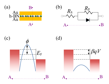
Based on atomistic simulations and measurements, the transport during the different resistive switching states of hBN MIM-like devices (cf. Fig. 1(a)) has been associated to the formation of conducting filaments enabled by boron vacancies [7], [14]-[16]. The electronic band diagram of the device is schematically represented by Figs. 1(c) and (d). At the high-resistance state (HRS) the conducting filaments form a narrow path and hence a potential barrier due to the confinement effect on electrons passing through it arises (cf. Fig. 1(c)). On the other hand, a wide constriction implies no barrier for the electrons as shown in Fig. 1(d), i.e., a low-resistance state (LRS) is considered.
A practical description of the scenario described above is provided by the quantum point contact model based on the Landauer transport equation [17]. Hence, the current-voltage characteristics of hBN switches is described here by a Landauer-based compact model given by [14], [17]
| (1) |
where is the applied voltage, with as the quantum conductance ( for one transmission mode) and as the number of fully formed conducting filaments; with as the element charge, as the number of independent conducting filaments, as the Planck’s constant and and are parameters related to the width and height, respectively, of a confinement-related potential barrier [14] (cf. Fig. 1(c)); is a series resistance embracing non-broken hBN layers, metal-contact layers and extrinsic phenomena. Eq. (1) is a trascendental function for and it can be related to an equivalent circuit (EC) conformed by a resistance (first term) in parallel with a diode (second term) and both in series with as seen in Fig. 1(b).
| (2) |
where , and is the Lambert function. Details on the derivation of the model have been provided elsewhere [14], [17]. Notice that Eq. (2) is only valid if the intrinsic potentials are lower than the barrier height, i.e., and if an asymmetric constriction is considered111This implies that the applied bias drops entirely at the source side of the constriction [14].
Eq. (2) describes the current at HRS where both effects, a resistance related to the the 2D material and the transport through a potential barrier, are present. However, for LRS, the latter effect has no impact on the current (, see Fig. 1(d)) due to the formation of a very wide energy constriction, i.e., , and hence Eq. (1) reduces to [14]
| (3) |
II-B Dynamic response
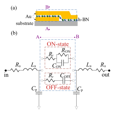
The cross-section of an hexagonal borond nitride RF switches, similar as the ones demonstrated in the literature [7], [9], [11], is shown in Fig. 2(a). As a first approximation for the description of the high-frequency performance of 2D RF switches, the small-signal EC shown in Fig. 2(b) has been used. The intrinsic part of the EC changes according to the switch state and it can be derived from the circuit shown in Fig. 1(b) by considering the small-signal EC of the diode [21]. For the ON-state, a parallel array of a resistance and a capacitor have been used to represent the resistance and a non-negligible charge, respectively, within the activated MIM structure. The latter arrangement is obtained by considering the small-signal EC of the diode (cf. Fig. 1(b)) and hence is approximately equal to the voltage-dependent resistance of the diode222This approximation is guaranteed by () being much higher than the voltage-dependent diode resistance (with a lower value) to which it is in parallel with.. A capacitor represents the electrostatic coupling between device materials in the OFF-state. For both states in the intrinsic part, a residual series resistance has been included here in contrast to previous works in the literature [6, 7], [10], [22] where such effect has been neglected. For the ON-state, i.e., at LRS, , whereas at the OFF-state, i.e., at HRS, is a fitting parameter. Two aspects should be noticed for at OFF-state: (i) it is required to prevent infinite isolation at low frequency, and (ii) the value differs from the one used for in Eq. (2) due to a possible independent measurement of DC and RF characteristics, i.e., different cycles might be used to obtain the corresponding characteristics. The extrinsic network is comprised by a parasistic capacitor , an access resistance and an inductance associated to each port.
The -parameter for a two-port reciprocal and symmetrical network, such as the one describing the RF nanoswitch (c.f. Fig. 2), in terms of the -parameters is given by [23]
| (4) |
where is the characteristic impedance, whereas the impedance terms for the device with extrinsic contributions are
| (5) |
and
| (6) |
with
| (7) |
the access impedance , the extrinsic impedance due to pads electrostatic coupling and the intrinsic impedance as
| (8) |
where is the angular frequency with as the operation frequency. By using Eqs. (5)-(8), and the corresponding values of the elements, in Eq. (4), the extrinsic insertion loss (ON-state) and isolation (OFF-state) are obtained. Notice that by doing the corresponding parameter transformation [23], Eq. (4) is equivalent to the one given for conventional lateral RF switches considering ABCD parameters [24]333The expressions reported for , obtained with ABCD parameters, in [6] and [7] have both a typo in the second term of the denominator.
On the other hand, the intrinsic part of the 2D RF switch can be considered as a series impedance block and hence, the intrinsic insertion loss and isolation can be obtained by [25]
| (9) |
depending on whether is defined for the ON- or OFF-state, respectively. Notice that the approach presented here considers the contribution of in the expressions of both extrinsic and intrinsic insertion loss in contrast to previous studies [5]-[7] where this effect has been neglected.
The extrinsic and intrinsic return loss [23], considering the EC in Fig. 2 and Eqs. (5)-(8), can be calculated from
| (10) |
and
| (11) |
respectively, at ON-state.
III Results and discussion
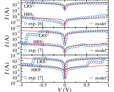
The modeling approach presented above has been applied to describe the experimental I-V performance, RF insertion loss and RF isolation of fabricated hBN RF switches [6, 7] with different device footprints. Details on the fabrication processes and measurements have been presented elsewhere [6, 7]. I-V characteristics of hBN RF switches have been successfully described by the model at both states, i.e., HRS and LRS by Eqs. (2) and (3), respectively, as shown in Fig. 3. Notice that the intrinsic voltage is lower than the barrier height in all devices, i.e., Eq. (2) is valid. The large difference in the value of at ON-state (LRS) and OFF-state (HRS) is due to the potential step affecting the transport differently at each case.
Regarding the small-signal response, Table I collects the intrinsic parameter values used here for describing the experimental data of 2D RF switches. Values of and obtained here are in good agreement with the reported ones in [6] and for the smallest device in [7]. For the largest device in [7], and have been obtained by considering a correct description of the RF power handling feature of the switch. values have not been reported previously for ECs of hBN switches in the literature and are obtained here by considering a correct description of in the ON-state for each switch. The values of obtained for the hBN devices are similar to the ones reported elsewhere for fabricated hBN-based MIMs, i.e., few [27, 28]. Furthermore, this capacitive effect at ON-state has not been observed in other 2D monolayer RF switches [4], [5] and hence it is suggested here to be associated to the charge storaged within the hBN layer during the filament-based resistive switching [15] rather than to the thickness of the monolayer as suggested elsewhere [6]. A further discussion of the intrinsic mechanism of the resisitive switching mechanism in hBN is out of the scope of this work, however, interested readers are directed to [15].
| [ref.] | device area () | () | () | () | ( |
| [6] | |||||
| [7] | |||||
| [7] |
The EC extrinsic network for all devices has been calibrated to the electromagnetic simulations of the OPEN-structure presented in [6]. The obtained values of and (cf. Fig. 4(a)) are equal to and , respectively. An of corresponds to an average value of a minimum and a maximum limit of a gold access pad, such as the one used in [6, 7], considering a coplanar waveguide and an isolated microstrip, respectively [26].
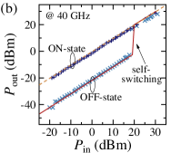
The EC describes the experimental RF power handling in both ON- and OFF-state of the device in [7] at , as well as its self-switching, as shown in Fig. 4(b). The self-switching from OFF- to ON-state is achieved with the EC by considering a transition from to (see values in Table I) which, along with the accurate description of ON-state results, confirms the value proposed here for the latter element.
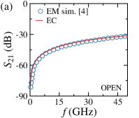
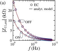
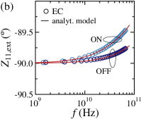
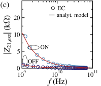
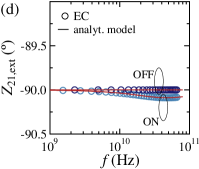
In order to validate the expressions considering extrinsic elements, a comparison with results of the experimentally-calibrated EC has been performed for the devices under study. Eqs. (5) and (6) reproduce properly the TCAD results of the impedance parameters (magnitude and phase) obtained here (with both extrinsic and intrinsic elements), regardless the state of the switch, for the smallest hBN device presented in [7] as shown in Fig. 5.
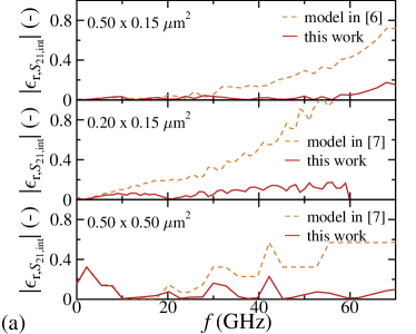
The comparison between de-embedded (intrinsic) experimental and the different models, namely the one presented here (cf. Eq. (9)) and the one in the corresponding original reference [6], [7], is shown in Fig. 6444Extrinsic elements are not considered in the experimental data nor in the modeling results.. The modeling approach presented here differs from the previous reported model in [6], [7] since the former one considers (for the ON-state) and (for both states) in the EC in contrast to the latter one where both of these elements are neglected.
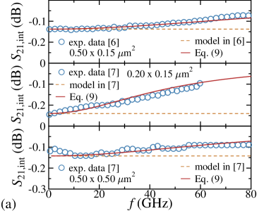
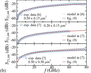
For the device in [6] and the smallest one in [7], the impact of is minimum in the description of the insertion loss (cf. Fig. 6(b)). However, for the largest device in [7] the model used here including fits better the experimental data in contrast to the lumped EC not considering this element (cf. Fig. 8(b) in Appendix). On the other hand, for the ON-state, the increase of with frequency is not captured by the pure resistive intrinsic part of the models reported in [6] and [7]. Eq. (9) obtained here is able to reproduce such unique attractive feature of RF hBN switches by considering a capacitance different to zero in the intrinsic part of the device (cf. Eq. (8)), in contrast to the conventional approaches developed for other switches not presenting such effect. The relative error of each modeling approach with respect to the experimental data is shown in Fig. 8 in the Appendix where the higher accuracy of the model presented here with respect to others reported in the literature is observed, e.g.,the average (over the analyzed frequency range) of (in percentage) for at ON-state is of with the model proposed here and with other approaches for the devices in [6] and [7], respectively.
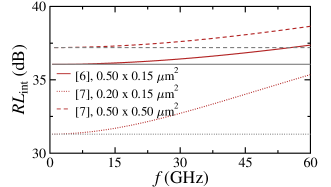
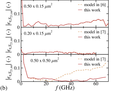
The return loss, an important factor for RF switches [24], not reported experimentally for any of the devices under study [6], [7], has been calculated here by using Eq. (11). Fig. 7 shows that the improves with the frequency due to the effect of the capacitance at ON-state whereas the device with largest area in [7] has the highest of the three hBN switches.
IV Conclusion
The static characteristics of hBN-based MIM-like structures, intended for RF applications, have been described for the first time here at both resistive states by using a physics-based equivalent circuit and the corresponding equations. Furthermore, the dynamic performance of 2D RF switches based on hBN has been precisely modeled here by considering an intrinsic charge contribution -via - related to the storaged charge within this 2D material during the filament-based resistive switching mechanism. An analysis of the equivalent circuit considering such contribution yields straightforward expressions used to describe a unique increase with frequency of the parameter of RF hBN switches. Both the EC and the derived equations for impedance and scattering parameters are able to describe experimental data of three different devices. The relative error of the return loss and the insertion loss shows the higher accuracy of the approach discussed here with respect to other previously used models. The expressions obtained here for the dynamic performance of hBN switches aim to boost the modeling and analysis of these devices as well as their use in circuit design by considering a physical phenomenon represented by , neglected in previous works, in their equivalent circuit.
Appendix
The relative error of the two dynamic modeling approaches, the one with and (proposed here) and the oftenly used one without such elements are shown in Fig. 8 for at both states (cf. Fig. 6) with respect to the experimental data.
Acknowledgements
The authors thank Deji Akinwande from University of Texas and Enrique Miranda from Universitat Autònoma de Barcelona for fruitful discussions.
References
- [1] M. Lanza, A. Sebastian, W. D. Lu, M. Le Gallo, M.-F. Chang, D. Akinwande, F. M. Puglisi, H. N. Alshareef, M. Liu, J. B. Roldan, ”Memristive technologies for data storage, computation, encryption, and radio-frequency communication”, Science, vol. 376, no. 6597, Jun. 2022.
- [2] K. Qian, R. Y. Tay, V. C. Nguyen, J. Wang, G. Cai, T. Chen, E. H. T. Teo, P. S. Lee, ”Hexagonal Boron Nitride Thin Film for Flexible Resistive Memory Applications”, Advanced Functional Materials, vol. 26, pp. 2176-2184, Feb. 2016. DOI: 10.1002/adfm.20150477
- [3] N. Wainstein, G. Adam, E. Yalon, S. Kvatinsky, ”Radio Frequency Switches Based on Emerging Resistive Memory Technologies: A Survey”, Proceedings of the IEEE, vol. 109, no. 1, pp. 77-95, Jan. 2021. DOI: 10.1109/JPROC.2020.3011953
- [4] R. Ge, X. Wu, M. Kim, J. Shi, S. Sonde, L. Tao, Y. Zhang, J. C. Lee, D. Akinwande, ”Atomristor: Nonvolatile Resistance Switching in Atomic Sheets of Transition Metal Dichalcogenides”, Nano Letters, vol. 18, pp. 434-441, 2018. DOI: 10.1021/acs.nanolett.7b04342
- [5] M. Kim, R. Ge, X. Wu, X. Lan, J. Tice, J. C. Lee, D. Akinwande, ”Zero-static power radio-frequency switches based on MoS2 atomristors”, Nature Communications, vol. 9, 2524, 2018. DOI: 10.1038/s41467-018-04934-x
- [6] M. Kim, E. Pallecchi, R. Ge, X. Wu, V. Avramovic, E. Okada, J. C. Lee, H. Happy, D. Akinwande, ”Non-volatile RF and mm-wave Switches Based on Monolayer hBN”, in Proc. IEEE International Electron Devices Meeting (IEDM), pp. 9.5.1-9.5.4, Dec. 2019. DOI: 10.1109/IEDM19573.2019.8993470.
- [7] M. Kim, E. Pallecchi, R. Ge, X. Wu, G. Ducournau, J. C. Lee, H. Happy, D. Akinwande, ”Analogue switches made from boron nitride monolayers for application in 5G and terahertz communication systems”, Nature Electronics, vol. 3, pp. 479-485, Aug. 2020. DOI: 10.1038/s41928-020-0416-x
- [8] M. Kim, E. Pallecchi, H. Happy, D. Akinwande, ”Single-Pole-Double-Throw RF switches based on monolayer MoS2”, in Proc. IEEE Device Research Conference, Jun. 2021. DOI: 10.1109/DRC52342.2021.9467136
- [9] M. Kim, G. Ducournau, S. Skrzypczak, S. J. Yang, P. Szriftgiser, N. Wainstein, K. Stern, H. Happy, E. Yalon, E. Pallecchi, D. Akinwande, ”Monolayer molybdenum disulfide switches for 6G communication systems”, Nature Electronics, May 2022. DOI: 10.1038/s41928-022-00766-2
- [10] S. J. Yang, F. Makal, P. Peterson, J. Alikpala, C. J. Luth, S. K. Banerjee, A. Roessler, D. Akinwande, ”D-band frequency memristor switch based on monolayer boron nitride”, in Proc. IEEE Device Research Conference, Columbus, OH, USA, Jun. 2022. DOI: 10.1109/DRC55272.2022.9855801
- [11] S. J. Yang, M. M. Dahan, O. Levit, F. Makal, P. Peterson, J. Alikpala, SS T. Nibhanupudi, C. J. Luth, S. K. Banerjee, M. Kim, A. Roessler, E. Yalon, D. Akinwande, ”Reconfigurable Low-Voltage Hexagonal Boron Nitride Nonvolatile Switches for Millimeter-Wave Wireless Communications”, Nano Letters, vol. 23, no. 4, pp. 1152-1158, Jan. 2023. DOI: 10.1021/acs.nanolett.2c03565.
- [12] A. Laturia, M. L. Van de Put, W. G. Vandenberghe, ”Dielectric properties of hexagonal boron nitride and transition metal dichalcogenides: from monolayer to bulk”, npj 2D Materials and Applications, vol. 2, Feb. 2018. DOI: 10.1038/s41699-018-0050-x
- [13] Z. Ma, C. C. Prawoto, S. Li, Z. Ahmed, L. Zhang, M. Chan, ”Current Conduction Mechanisms in h-BN as a Dielectric Material”, in Proc. IEEE International Conference on Electron Devices and Solid State Circuits (EDSSC), Shenzhen, China, Jun. 2018. DOI: 10.1109/EDSSC.2018.8487119
- [14] C. Pan, E. Miranda, M. A. Villena, N. Xiao, X. Jing, X. Xie, T. Wu, F. Hui, Y. Shi, M. Lanza, ”Model for multi-filamentary conduction in graphene/hexagonal-boron-nitride/graphene based resistive switching devices”, 2D Materials, vol. 4, no. 2, 025099, May 2017. DOI: 10.1088/2053-1583/aa7129
- [15] X. Wu, R. Ge, P.-A. Chen, H. Chou, Z. Zhang, Y. Zhang, S. Banerjee, M.-H. Chiang, J. C. Lee, D. Akinwande, ”Thinnest Nonvolatile Memory Based on Monolayer h-BN”, Advanced Materials, vol. 31, 1806790, 2019. DOI: 10.1002/adma.201806790
- [16] S. Mitra, S. Mahapatra, ”Insights into nonvolatile resistive switching in monolayer hexagonal boron nitride”, Journal of Applied Physics, vol. 132, 224302, Dec. 2022. DOI: 10.1063/5.0128682
- [17] J. v. Ruitenbeek, M. Morales Masis, E. Miranda, ”Quantum Point Contact Conduction” in Resistive Switching (eds D. Ielmini and R. Waser), Wiley‐VCH Verlag GmbH & Co. KGaA, Weinheim, Germany, Jan. 2016. DOI: 10.1002/9783527680870.ch7.
- [18] E. Miranda, J. Suñé, C. Pan, M. Villena, N. Xiao, M. Lanza, ”Equivalent circuit model for the electron transport in 2D resistive switching material systems”, in Proc. IEEE European Solid-State Device Research Conference (ESSDERC), Leuven, Belguim, Sep. 2017. DOI: 10.1109/ESSDERC.2017.8066598
- [19] K. Zhu, X. Liang, B. Yuan, M. Villena, C. Wen, T. Wang, S. Chen, F. Hui, Y. Shi, M. Lanza ”Graphene-Boron Nitride-Graphene Cross-Point Memristors with Three Stable Resistive States”, ACS Applied Materials & Interfaces, vol. 11, pp. 37999-38005, Sep. 2019. DOI: 10.1021/acsami.9b04412
- [20] M. A. Villena, F. Hui, X. Liang, Y. Shi, B. Yuan, X. Jing, K. Zhua, S. Chen, M. Lanza, ”Variability of metal/h-BN/metal memristors grown via chemical vapor deposition on different materials”, Microelectronics Reliability, vol. 102, 113410, Nov. 2019. DOI: 10.1016/j.microrel.2019.113410
- [21] A. M. Cowley, H. O. Sorensen, “Quantitative comparison of solid-state microwave detectors,” IEEE Transactions on Microwave Theory and Techniques, vol. MTT-14, no. 12, pp. 588–602, Dec. 1966. DOI: 10.1109/TMTT.1966.1126337
- [22] O. Jordán-Garcia, E. Ramírez-García, D. Jiménez, A. Pacheco-Sanchez, “Lumped model-based analysis of hBN RF switches”, in Proc. IEEE Latin American Electron Devices Conference (LAEDC), Puebla, Mexico, Jul. 2022. DOI: 10.1109/LAEDC54796.2022.9907772
- [23] D. M. Pozar, ”Microwave engineering”, Wiley, Hoboken, NJ, USA, 2005.
- [24] A. Q. Liu, ”RF MEMS Switches and Integrated Switching Circuits”, vol. 5, Springer Science & Business Media, Philadelphia, PA, USA, 2010.
- [25] F. Caspers, ”RF engineering basic concepts: S-parameters”, CERN Yellow Report CERN-2011-007, pp. 67-93, 2010. Available online in https://arxiv.org/abs/1201.2346
- [26] R. Anholt, S. Swirhun, ”Equivalent-circuit parameter extraction for cold GaAs MESFET’s”, IEEE Transactions on Microwave Theory and Techniques, vol. 39, no. 7, pp. 1243-1247, Jul. 1991. DOI: 10.1109/22.85396
- [27] F. Ahmed, S. Heo, Z. Yang, F. Ali, C. H. Ra, H.-I. Lee, T. Taniguchi, J. Hone, B. H. Lee, W. J. Yoo, ”Dielectric Dispersion and High Field Response of Multilayer Hexagonal Boron Nitride”, Advanced Functional Materials, vol. 28, no. 40, 1894235, Oct. 2018. DOI: 10.1002/adfm.201804235
- [28] Y. He, Y. Li, M. Isarraraz, P. Pena, J. Tran, L. Xu, H. Tian, T. Yang, P. Wei, C. S. Ozkan, M. Ozkan, J. Liu, ”Robust Nanocapacitors Based on Wafer-Scale Single-Crystal Hexagonal Boron Nitride Monolayer Films”, ACS Applied Nano Materials, vol. 4, no. 6, pp. 5685-5695, Jun. 2021. DOI: 10.1021/acsanm.1c00298