Emergence of Rashba-spin-valley state in two-dimensional strained bismuth oxychalcogenides Bi2O2Se
Abstract
The experimental evidence of the ultra-high electron mobility and strong spin-orbit coupling in the two-dimensional (2D) layered bismuth-based oxyselenide, Bi2O2Se, makes it a potential material for spintronic devices. However, its spin-related properties have not been extensively studied due to the centrosymmetric nature of its crystal structure. By using first-principles density-functional theory calculation, this study reports the emergence of Rashba-spin-valley states in Bi2O2Se monolayer (ML). Breaking the crystal inversion symmetry of Bi2O2Se ML using an external electric field enables the Rashba-spin-valley formation, causing the appearance of the Rashba-type splitting around the valley and spin-valley coupling at the valleys located near the middle of line. In addition to the typical Rashba-type spin textures around the valley, the study also observed in-plane unidirectional spin textures around the valleys, which is a rare phenomenon in 2D materials. The observed Rashba-spin-valley states are driven by the lowering point group symmetry of the crystal from to enforced by the electric field, as clarified through model derived from symmetry analysis. More importantly, tuning the Rashba and spin-valley states by using biaxial strain offers a promising route to regulate the spin textures and spin splitting preventing the electron from back-scattering in spin transport. Finally, we proposed a more realistic system, namely, Bi2O2Se ML/SrTiO3 (001) heterointerface that supports the strong Rashba-spin-valley states and highlighting the potential of the Bi2O2Se ML for future spintronics and valleytronics-based devices.
pacs:
Valid PACS appear hereI INTRODUCTION
The correlation between the electron spin and orbital degrees of freedom is a fundamental concept in a range of emerging areas, such as spintronics and valleytronics [1, 2, 3]. The examination of the symmetry of crystalline solids is critical in comprehending the physical properties of these new fields. For an instant, in a system that possesses both inversion and time-reversal symmetry, the doubly degenerate electronic bands are preserved throughout the first Brillouin zone (FBZ) even in the presence of the spin-orbit coupling (SOC), known as Kramer’s spin degeneracy. When the inversion symmetry is broken, the SOC induces the momentum-dependent spin–orbit field (SOF) and lifts the band degeneracy through the so-called Rashba [4] and Dresselhaus [5] effects. During the past decade, the Rashba-Dresselhauss effect has been the subject of intense research due to its potential applications in the emergent field of spintronics [6, 7]. In particular, the Rashba effect can manipulate the polarized spins by the external electric field [8] and thus holds promise for realizing spin field effect transistors (FETs) in experiments [9].
In addition, an intriguing phenomenon arises when the time-reversal symmetry of crystalline solids is broken. In such cases, the absence of inversion symmetry, combined with the SOC, gives rise to the spin-valley contrasting effect [2, 10]. Typically, the term valley refers to the energy extrema points in momentum space that represents a binary index for low-energy carriers, which is robust to the scattering by smooth deformations and long-wavelength phonons [10, 11]. The valley degree of freedom is potentially utilized to store and carry information, leading to conceptual electronic applications known as valleytronics[12, 13]. Moreover, utilization of the spin-valley contrasting effect gives rise to topological valley transport properties such as photo-induced charge Hall effect, valley Hall effect, and spin Hall effect under zero magnetic field [10, 14, 15]. Several promising systems for hosting the spin-valley contrasting effect have been reported in two-dimensional (2D) systems, including the family of transition metal dichalcogenides (TMDCs) (=W, Mo; =S, Se, Te) monolayer (ML) [10, 14, 15] and a class of septuple-atomic-layer MXenes (=W, Mo; = Si, Ge; = N, P, As Te) ML [16, 17, 18]. Here, symmetry of the TMDCs ML enforces the occurrence of the large spin splitting located at the valley in the FBZ, exhibiting valley-contrasting spin polarization perpendicular to the 2D plane. This effect has been evidenced by its unique optical and transport characteristics, including valley-dependent circular dichroic photoluminescence [19, 20] and nonreciprocal charge transport [21].
In some systems with multiple well-separated valleys, the Rashba and spin-valley effects can both be observed. In such cases, coupling between the Rashba and spin-valley states can occur, resulting in Rashba-flavored spin-valley states. These states enable non-dissipative transport of both spin and valley degrees of freedom by utilizing the position of the Rashba and spin-valley states near the Fermi level. Typically, Rashba states produce a pair of spin-polarized bands in -space with opposite chiral in-plane spin textures, which allows electrons to back-scatter and greatly reduces the efficiency of spin transport [22, 23]. In contrast, back-scattering is suppressed in spin-valley states due to their unidirectional out-of-plane spin textures [24, 25]. The Rashba-spin-valley states have been observed in various 2D ML structures with in-plane mirror symmetry breaking, such as Janus TMDCs (=W, Mo; =S, Se, Te) ML [26, 27, 28], Janus MXenes (=W, Mo; = Si, Ge; = N, P, As Te) ML [29, 30], Janus Titanium dihalide Ti ( = Cl, Br, I) ML [31] and buckled hexagonal h-N (=V, Nb, and Ta) ML [32]. However, the close energy proximity between the Rashba and spin-valley states in these systems may induce interference between in-plane and out-of-plane spin textures, resulting in low efficiency of spin transport. Recently, it has been reported that 2D layered centrosymmetric black arsenic also hosts Rashba-spin valley states that can be controlled by electrostatic gating [33]. However, the light atomic weight of arsenic leads to a small spin splitting of the Rashba-spin valley states.
This study utilizes first-principles density-functional theory (DFT) calculations to show that the Rashba-spin-valley states emerge in 2D bismuth oxyselenide, Bi2O2Se. Recently, 2D ultrathin layered Bi2O2Se has been successfully synthesized, exhibiting the strong SOC interaction [34, 35] and superior transport properties such as ultra-high Hall electron mobility [36, 37, 38, 39], making the achievement of Rashba-spin-valley states in this material significant for the development of spintronics and valleytronics applications. We find that breaking the crystal inversion symmetry of 2D Bi2O2Se ML using an external electric field leads to the Rashba-spin-valley formation exhibiting the Rashba-types splitting around the valley and spin-valley coupling at valleys located near the middle of the line. Unlike previous studies, unidirectional in-plane spin textures around the valleys are observed, in addition to conventional Rashba-type spin textures around the valley. These spin textures are driven by the electric field-induced lowering of crystal symmetry from to point group, as demonstrated through the model derived from symmetry analysis. More interestingly, manipulating the Rashba and spin-valley states through biaxial strain offers an efficient means of managing the spin textures and spin splitting, thereby hindering electron back-scattering in spin transport. We further propose a more realistic system, namely, Bi2O2Se ML/SrTiO3 (001) heterointerface, where the strong Rashba-spin-valley states is achieved. Since molecular beam epitaxy (MBE) of atomically thin Bi2O2Se film down to the ML structure grown on the SrTiO3 (001) substrate has been experimentally reported [40], observation of the Rashba effect on the Bi2O2Se ML/SrTiO3 (001) is expected to be realized in the near future. Therefore, the application of Bi2O2Se ML for spintronics and valleytronics devices is plausible.
II Model and Computational Details
To evaluate the structural, electronic, and spin-splitting-related properties of Bi2O2Se ML, we performed fully relativistic DFT calculations, where the SOC was taken into account self-consistently by using total momentum ()-dependent pseudo potentials [41]. We used norm-conserving pseudo-potentials and optimized pseudo-atomic localized basis functions in our DFT calculations implemented in the OpenMX code [42, 43, 44]. We apply the generalized gradient approximation of Perdew, Burke, and Ernzerhof (GGA-PBE) [45, 46] as an exchange-correlation functional. The linear combinations of multiple pseudo atomic orbitals (PAOs) generated using a confinement scheme were used as the basis functions [42, 43, 44]. A set of the PAOs basis functions was specified as Bi8.0-3221, Sr7.0-3221, Ti7.0-322, Se7.0-322, O6.0-222, and H6.0-22, where 8.0, 7.0, 7.0, 7.0, 6.0, and 6.0 are the cutoff radii (in bohrs) of Bi, Sr, Ti, Se, O, and H atoms, respectively. Here, the integers after , , , and indicate the radial multiplicity of each angular momentum component. The accuracy of the basis functions, as well as pseudo-potentials we used, were carefully bench-marked by the delta gauge method [47]. We make a periodic slab model with a sufficiently large vacuum layer (25 Å) to avoid interaction between adjacent layers. We used an -point and real space grids corresponding to energy cutoffs larger than 350 Ry to obtain the converged results of the self-consistent field (SCF) loops. The energy convergence criterion of eV was used. Phonon dispersion band is used to evaluate the dynamical stability of the Bi2O2Se ML obtained by using ALAMODE code [48] based on the force constants obtained from the OpenMX code calculations.
To provide a more realistic system, we built a heterostructure where SrTiO3 [001] substrate is applied on Bi2O2Se ML. Here, SrTiO3 [001] surface was modeled using eight layers slab. Two stables formation of Bi2O2Se ML/SrTiO3 [001] interface is considered, i.e., (i) Se-SrO and (ii) Se-TiO2 interface termination. The stability of Bi2O2Se ML/SrTiO3 [001] interface was evaluated by calculating the cohesive energy () through the following relation,
| (1) |
where , , and are the total energy of Bi2O2Se ML/SrTiO3 [001], Bi2O2Se ML surface, and isolate SrTiO3 [001] surface, respectively, while represents surface area.
To study the Rashba-spin valley effect, we applied a uniform external electric field on Bi2O2Se ML along the -direction modeled by a sawtooth waveform during the SCF calculation and geometry optimization. We calculated the spin textures in the momentum -space by deducing the spin vector components (, , ) in the reciprocal lattice vector from the spin density matrix. By using the spinor Bloch wave function, , obtained from the DFT calculations after the self-consistent field (SCF) is achieved, we calculate the spin density matrix, , by using the following equation [49, 50],
| (2) |
where is the overlap integral of the -th and -th localized orbitals, is expansion coefficient, () is the spin index ( or ), is the band index, and is the -th lattice vector. This method has been successfully applied in our recent studies on various 2D materials[51, 52, 53, 54, 55, 56].
III Results and Discussion
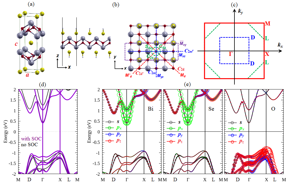
First, we examine the structural properties of Bi2O2Se ML. The geometry of the bulk and 2D ML structures are shown in Figs. 1(a)-(b), while the corresponding 2D FBZ is illustrated in Fig. 1(c). The layered Bi2O2Se crystallizes in a tetragonal structure with space group [Fig. 1(a)], consisted of alternating stacking of positively charged [Bi2O2] layers and negatively charged [Se2] layers with weak electrostatic interactions [36]. The 2D ML structure of Bi2O2Se can be constructed by separating the crystal in the direction (-direction) through the ionic bonds between [Bi2O2]2+ and Se2- layers [Fig. 1(b)]. Here, the Se2- layers terminate both the top and bottom surface MLs, thus preserving the inversion symmetry. Similar to its bulk counterpart, Bi2O2Se ML belongs to the point group symmetry [36, 57], generated by the following symmetry operations: , , , , , , , , , and . Here, is the identity operator, is the inversion symmetry, and represent the two-fold and four-fold rotations around the axis, respectively, and are the two-fold rotations around the dihedral and vertical mirror axis, respectively, is the four-fold rotations around the axis followed by reflection through the plane, is the glide mirror symmetry through the mirror plane followed by translation, is the vertical mirror symmetry through the and mirror plane, respectively, and are the dihedral mirror symmetry containing the axis and crossing the angle between and [Fig. 1(b)]. In our model, we applied hydrogen H-passivated configuration on Bi2O2Se ML for balancing the non-stoichiometry as used in the previous studies [58, 59, 60, 61]. We find that this structural configuration is dynamically stable as confirmed by phonon dispersion bands shown in Fig. S1 in the supplementary materials [62]. Nevertheless, the optimized in-plane lattice parameter of the ML (3.98 Å) is a bit larger than that of the bulk (3.91 Å), which agrees with prior findings [58, 59, 60, 61].
Fig. 1(d) depicts the electronic band structure of Bi2O2Se ML calculated with and without SOC. It demonstrates that the ML is a semiconductor having multiple valleys in its electronic band structures. Three valleys are observed at the conduction band, with the valley having the lowest energy, the valley located at the middle of the line, and the valley near the middle of the line [Fig. 1(d)]. On the contrary, the valence band is characterized by the , , and valleys, with the highest energy level located at the valleys. The valley in the conduction band mainly comes from the orbitals of the Bi and Se atoms, while the and valleys mostly originate from the mixing between and orbitals of the Bi and Se atoms [Fig. 1(e)]. On the contrary, orbital of the O atoms contributes dominantly to the , , and valley at the valence band. Since the conduction band minimum (CBM) and valence band maximum (CBM) is located at the and valleys, respectively, an indirect band gap is observed. The calculated value of the indirect band gap is 1.2 eV, which is in good agreement with previous theoretical reports [58, 60]. We noted here that the indirect band gap of the 2D ultra-thin Bi2O2Se has been previously reported experimentally by using optical measurement [36]. Although this indirect band gap is consistent-well with our calculations, the magnitude of the experimental band gap (1.95 eV) [36] is larger than that of our result (1.2 eV), which is due to the use of the GGA-PBE in our DFT calculations. However, the topological band curvature including the position of the CBM and VBM obtained in our calculations is consistent-well with the ARPES experiment [36, 38]. When the SOC is taken into account, the indirect band gap of Bi2O2Se ML decreases to 1.1 eV. Since the inversion symmetry is preserved in Bi2O2Se ML, all the bands are spin degenerated [see red line in Fig. 1(d)]. Thus, there is no spin-splitting observed on Bi2O2Se ML.
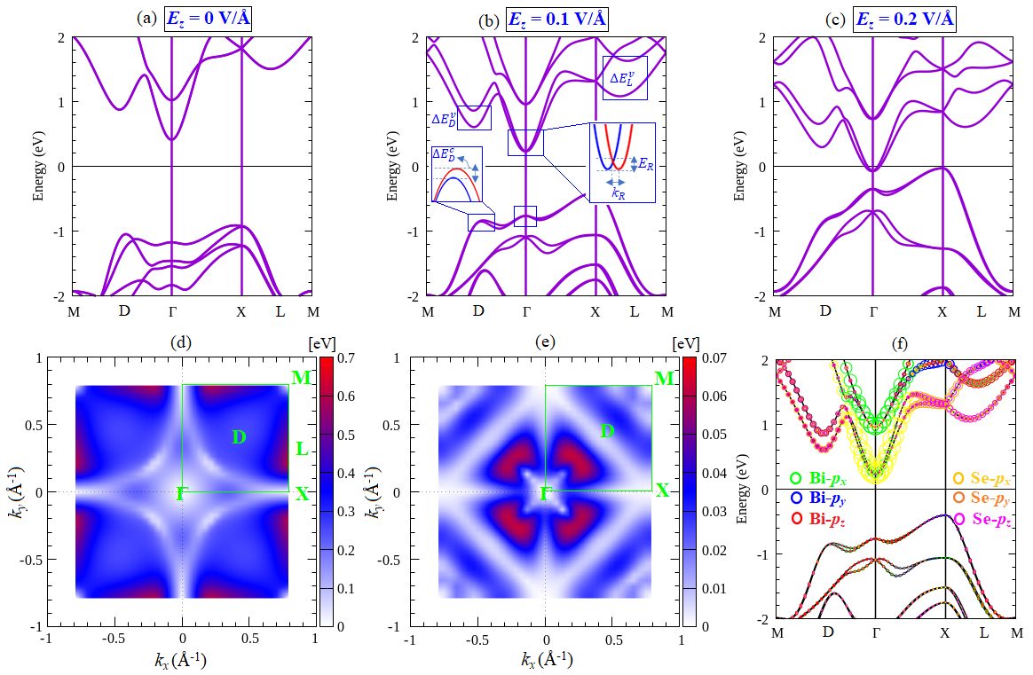
In order to observe spin splitting in a Bi2O2Se ML, an external electric field () perpendicular to the ML surface is employed to break the crystal inversion symmetry. We utilized electric fields reaching a magnitude of 0.2 V/Å, demonstrating thermodynamic stability as confirmed by the absence of imaginary frequency in the phonon dispersion; see Figs. S1 in the supplementary materials [62]. Figs. (2a)-(2c) illustrate evolution of the band structures of Bi2O2Se ML with different magnitudes of , revealing that when is smaller than 0.18 V/Å, the indirect band gap remains, but at larger of 0.18 V/Å, it becomes metallic. This change from an indirect semiconductor to a metallic state, which is similar to that previously reported on InSe ML [63] and bilayer phosphorene [64], is due to the strong coupling between the - orbitals of Bi, Se, and O atoms in both the CBM and VBM [refer to Fig. 1(e)]. Additionally, the breaking of inversion symmetry together with SOC generates spin-splitting bands throughout the FBZ, except for high symmetry points at , , and valleys, which remain time-reversible [see Figs. 2(b)-(c)]. Since the spin splitting is more prominent in the bands near the Fermi level [Figs. 2(b)-(c)], hence this paper primarily focuses on the spin-split bands at both the CBM and VBM.
| ML systems | (eV) | (eVÅ) | Reference | |||||||||
|---|---|---|---|---|---|---|---|---|---|---|---|---|
| Bi2O2Se | 0.32 ( valley, CBM) | 1.33 (CBM) | This work | |||||||||
| 0.68 ( valley, CBM) | ||||||||||||
| 0.11 ( valley, VBM) | 0.52 (VBM) | |||||||||||
| 2D Janus TMDCs | ||||||||||||
| MoSSe | 0.17 ( valley) | 0.07 | Ref.[26] | |||||||||
| WSTe | 0.49 ( valley) | 0.48 | Ref.[27] | |||||||||
| WSeTe | 0.45 ( valley) | 0.92 | Ref.[28] | |||||||||
| 2D Janus MXenes | ||||||||||||
| Mo(W)Si2PxAsy () | 0.14 - 0.51 ( valley) | 0.0 - 0.61 | Ref.[29] | |||||||||
| Mo(W)Ge2P2As2 | 0.14 - 0.47 ( valley) | 0.5 - 0.52 | Ref.[30] | |||||||||
| 2D Janus TiXY (= Cl, Br, I) | 0.04 - 0.06 ( valley) | 0.07 | Ref.[31] | |||||||||
| Other 2D materials | ||||||||||||
| BAs ML | 0.004 ( valley) | Ref.[33] | ||||||||||
| h-N (: V, Nb, Ta) | 0.01 - 0.11 ( valley) | 0.55 - 4.23 | Ref.[32] |
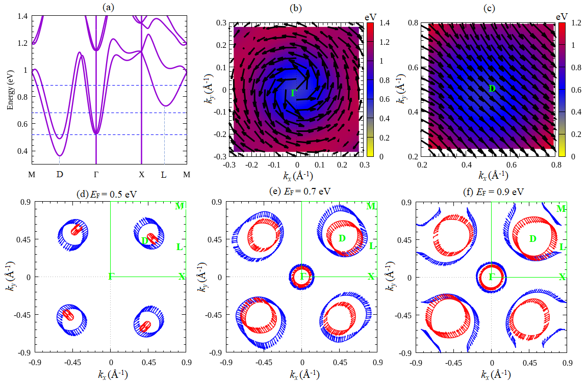
Figs. 2(d) and 2(e) depict the spin-splitting energy of a Bi2O2Se ML at an of 0.1 V/Å mapped throughout the FBZ and computed at the CBM and VBM, respectively. Our findings reveal that the spin splitting shows a highly isotropic character around the center of the FBZ ( valley), whereas it becomes strongly anisotropic near the edge of the FBZ ( and valleys). More interestingly, it is evident that large spin splittings occur in both the CBM and VBM, which is particularly visible at the valley ( eV; eV) and valley ( eV), and there are also an apparent the significant Rashba-type spin splitting around the valley [refer to Figs. 2(b), 2(d), and 2(e)]. Due to time-reversibility at the valley, the spin splittings are dictated to have opposite signs at the () and () valleys, giving rise to an effective coupling between spin and valley pseudospin. In addition, due to the close in energy between the and valleys, the Rashba-spin-valley states are achieved. Our calculations confirmed that the strong coupling between the and orbitals of Bi and Se atoms is responsible for inducing the substantial spin splitting at the and valleys, as evidenced by the orbital-resolved projected spin-split bands shown in Fig. 2(f). On the other hand, the Rashba spin splitting around the valley can be quantified by using the Rashba parameter obtained from the linear Rashba model through the relation, , where and are the Rashba energy and momentum offset, respectively [see the insert of Fig. 2(b)]. Then, we summarize the calculated results of the spin-splitting parameters (, , ) in Table I, and compare these results with a few selected 2D materials supported Rashba-spin-valley states. Notably, the spin splittings at the () and () valleys are comparable with that observed in various 2D Janus TMDCs ML [26, 27, 28] and Janus MXenes ML [29, 30], while the Rashba parameter around the valley is much larger than those 2D Janus systems. Additionally, all of the splitting parameters (, , and ) of the Rashba-spin-valley states are significantly larger than those observed on 2D Janus Ti (= Cl, Br, I) ML [31], 2D buckled h-N (: V, Nb, Ta) ML [32], and 2D BAs ML [33].
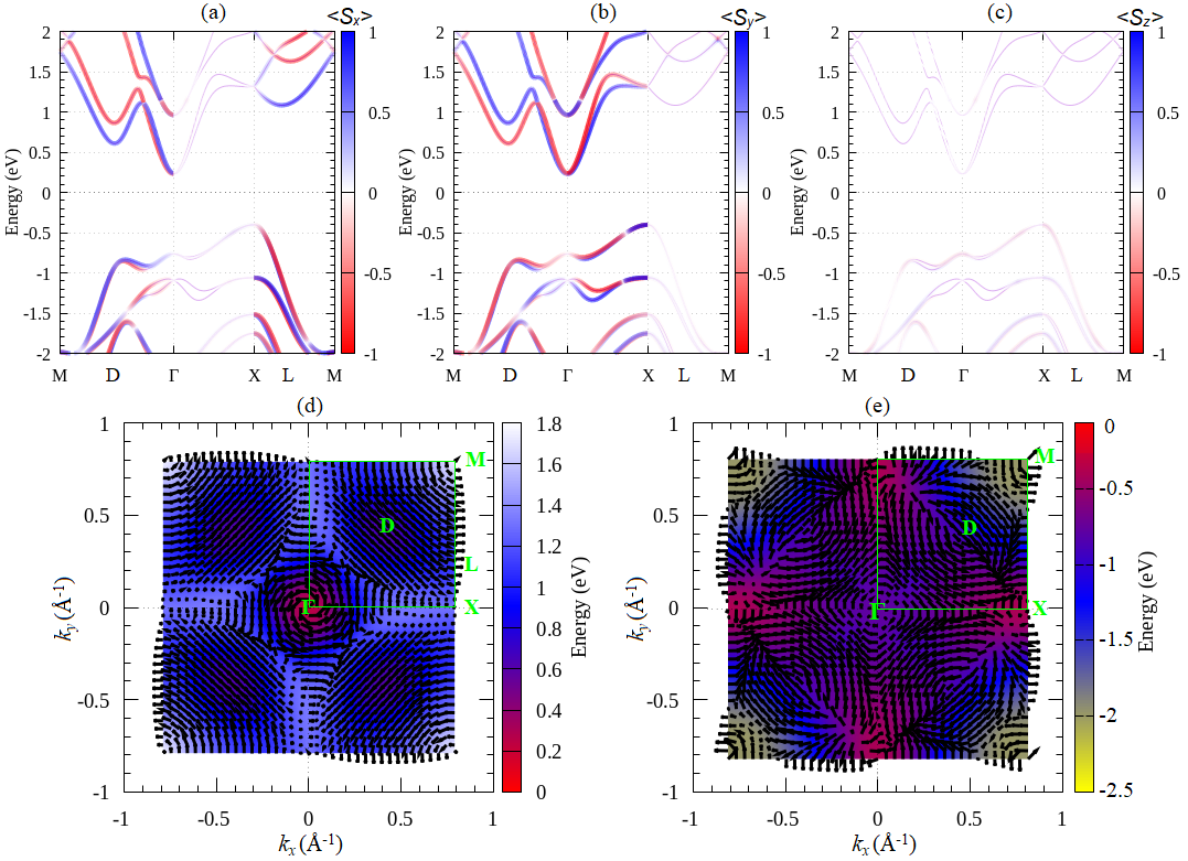
To gain a better understanding of the observed spin splitting of the Rashba-spin-valley states, we show in Figs. 3(a)-(c) expectation value of spin components (, , ) projected onto the spin-split bands near the Fermi level. Our findings show that the in-plane spin components (, ) are the dominant contributors to the spin-split bands, while the out-of-plane spin components () make only a negligible contribution. By calculating the energy-dependent spin textures projected onto the FBZ, we observed a typical Rashba spin rotation for the spin textures around the valleys, whereas the spin textures become unidirectional pointing along the direction which is parallel to the plane around the valleys [Figs. 3(d)-3(e)]. In particular, the observed unidirectional in-plane spin textures persistently around the valley are strongly different from the spin textures of the spin-valley states observed on various 2D valleytronics materials where the fully-out-of plane spin textures are observed around the valley [10, 14, 15, 16, 17, 18, 26, 27, 28, 29, 30, 31, 32]. The observed unidirectional in-plane spin textures in the present system lead to the formation of the persistent spin textures [65, 66, 53, 54, 55, 56, 67], which can prevent the electron from the back-scattering in spin transport and induces long-lived helical spin-wave mode through suppressing the Dyakonov spin-relaxation mechanism [22, 68, 69], which is promising for efficient spintronics.
| Symmetry operations | ||||||||
|---|---|---|---|---|---|---|---|---|
To clarify the origin of the observed spin splitting of Rashba-spin-valley states, we develop a two band dispersion model derived from the symmetry analysis. This band dispersion can be determined by identifying all terms allowed by symmetry so that , where represents symmetry operations associated with the wave vector group () corresponding to the high-symmetry point and time-reversal symmetry. The invariant Hamiltonian should satisfy the condition given below [70],
| (3) |
where is the matrix representation of operation belonging to point group of the wave vector .
As mentioned previously that Bi2O2Se ML belongs to PGS. When the electric field is applied, the symmetry of the crystal reduces to point group, where the following symmetry operations, , , , , and , remains. By using the transformation rules for the wave vector and spin vector given in Table II, the symmetry allowed SOC Hamiltonian up to third order term is given by
| (4) |
where is the Hamiltonian of the free electrons with eigenvalues , () is effective mass of electron evaluated from the band dispersion along the () directions, () are the components of the wave vector given regarding point taken as the origin, and are the Pauli matrices. Here, is the Rashba parameter which depends linearly on the electric field, . Moreover, the two last terms in Eq. (4) which depend on and are the third-order terms in , and are consistent with the derivation made by Vajna et al. [71] and Arras et al. [72]. The term in Eq. (4) has the usual form of the linear Rashba effect, which explains the isotropic in-plane Rashba spin rotation of the spin texture shown in Figs. 3(d)-(e). Moreover, near the valley, we find that , and we obtain that . This shows that the spin texture is oriented unidirectionally oriented in the in-plane direction parallel to the - plane, which is also consistent-well with the observed spin textures around the valley presented in Figs. 3(d)-(e).
Solving the eigen-value problem involving the Hamiltonian of Eq. (4), we obtain the spin-dependent eigenvalues []. Accordingly, the splitting energy of the spin-split bands, , can be evaluated along the and lines as follows,
| (5) |
and
| (6) |
with and . The parameters and can be obtained by numerically fitting of Eqs. (5) and (6) to the spin splitting energy along the and lines obtained from our DFT calculations, respectively. We find that the calculated and are 1.34 eVÅ(1.33 eVÅ) and 0.003 eVÅ3 (0.01 eVÅ3) for the spin-split bands at the CBM along the () line, respectively, while they are 0.524 eVÅ(0.517 eVÅ) and 0.01 eVÅ3 (0.004 eVÅ3) for the spin-split bands at the VBM along the () line, respectively. It is obvious that the obtained value of the cubic term parameters in both the and lines is too small compared with that of the linear-term parameter , indicating that the contribution of the higher-order correction is not essential. On the other hand, the calculated values of which give an almost isotropic linear-Rashba parameter () obtained from the higher order correction is fairly agreement with that obtained from the linear Rashba model; see Table I.
Thus far, we have found that the Rashba-spin-valley state is observed in the Bi2O2Se ML, which is expected that this ML is suitable for spintronics. However, considering the different features of the spin textures around the and valleys [Figs. 3(d)-(e)], interference of the spin-polarized states may occur, which is not beneficial for spin transport. Although the appearance of the persistent spin textures observed around the valleys may hold non-dissipative spin transport [22, 68, 69], it may be disturbed by the Rashba spin texture around the valley owing to the back-scattering of electrons [22, 23]. Therefore, suppressing the position of the Rashba states at the valley to be higher in energy than that of the spin-valley state at valley enables to prevent of the interference of the spin-polarized states. Since the multiple valleys observed near the band edges (CBM and VBM) are mostly characterized by the - coupling orbitals [Fig. 1(e)], the valley positions in the electronic band structures can be effectively modified by the application of the biaxial strain. In fact, the valley-dependent strain has been previously reported on two-dimensional black phosphorene-type structures such as group IV monochalcogenide [73, 74]. Therefore, manipulating the Rashba-spin-valley states through biaxial strain offers an efficient route of managing the spin textures and spin splitting, thereby hindering electron back-scattering in spin transport.
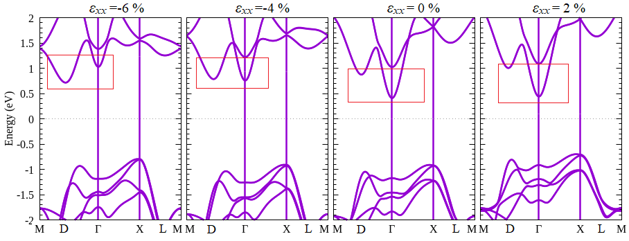
We then introduce a wide range of biaxial strain (up to %), which is applied to the in-plane lattice constant of the Bi2O2Se ML. We define the degree of in-plane biaxial strain as %, where is the unstrained in-plane lattice constant. Two different biaxial strains are studied, including the tensile strain, which increases the in-plane lattice constant , and the compressive strain, which decreases . Our calculated results of the optimized structures revealed that these biaxial strains sustain the crystal symmetry and maintain the dynamical stability of the Bi2O2ML as evidenced by the phonon dispersion bands depicted in Fig. S1 of the supplementary materials [62]. The strain-dependent of electronic band structures of the Bi2O2Se ML under different strain conditions is shown in Fig. 4. Consistent with previous reports [58, 60, 61], it is revealed that the strained ML remains semiconductor at large strain up to %. Under the tensile strain, an indirect band gap from valley (CBM) to valley (VBM) preserves similar to that of the equilibrium case. Conversely, the CBM starts to shift from the to valleys under the compressive strain larger than %. For the case of %, the valley is located much lower in energy than that of the valley at the CBM with a different energy of 0.42 eV. However, at the VBM, it is observed that the energy shift of the valley exceeds that of the valley by up to 0.23 eV. The decreasing (increasing) energy level of the valley with respect to the valley in the CBM (VBM) is expected to be useful for the spintronics since the spin texture of the spin-valley state around the valley could induce the spin-polarized states with minimal interference from the Rashba state around the valley.
To clarify this, we further apply an external electric field of 0.2 V/Å on the Bi2O2Se ML with % to observe the properties of the spin-polarized states. Concerning the large splitting bands at the CBM [Fig. 5(a)], we confirmed the presence of Rashba spin textures around the valley [Fig. 5(b)] and in-plane persistent spin textures around the valleys [Fig. 5(c)]. By comparing spin textures calculated at different constant energy cuts of the Fermi line () presented in Figs. 5(d)-(f), we clarified the possible interference of the spin-polarized states around the and valleys. At eV, all spin textures had a unidirectional in-plane orientation parallel to the plane, indicating that the spin-polarized states were achieved without any back-scattering. However, at larger [Figs. 5(e)-(f)], the mixing of spin textures around the and valleys resulted in the interference of spin-polarized states. Remarkably, non-dissipative spin transport can be achieved by tuning the position of the in the strained Bi2O2Se ML, which is important for operating spintronics devices.
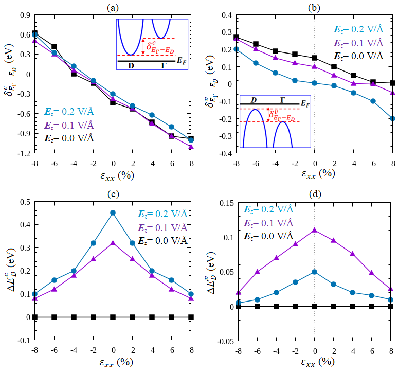
Now, we discuss the strain-electric field-dependent of the - valley positions as well as their spin-splitting energy. Figs. 6(a) and 6(b) show the energy difference of the and valleys with respect to the Fermi level () under the different strain and electric field [see the insert of Figs. 6(a)-(b) for the schematic view of ]. It is revealed that exhibit similar trends in both the CBM and VBM under different strain-electric field conditions. At the CBM, the positive value of is achieved under the compressive biaxial strain started from % and increases in magnitude under the increasing of the compressive biaxial strain and electric fields [Fig. (6a)]. Here, the CBM is mostly occupied by the valley states. Accordingly, the spin-polarized states are driven by the in-plane persistent spin texture suppressing the back-scattering of electrons and resulting in a highly efficient spin transport. On the other hand, the value of becomes negative when the tensile strain is applied, making the position of the CBM occupied by the valley state. Therefore, the spin-polarized states experience back-scattering due to the presence of the Rashba spin textures around the valley, and hence significantly reduces the efficiency of the spin transport. Since the similar trend of also holds for in the VBM [Fig. 6(b)], the similar character of the spin-polarized states is also expected. Considering the fact that the spin-splitting energy at the valley in both the CBM and VBM is tunable by the strain and electric field [Figs. 6(c)-6(d)], thus the present systems can be used as a promising platform for spintronic devices.
| Termination systems | (eV) | (eV) | (eV) | (eVÅ) | (eVÅ) | ||||||||||
|---|---|---|---|---|---|---|---|---|---|---|---|---|---|---|---|
| Se-SrO | 0.11 | 0.09 | 0.24 | 0.025 | 0.042 | ||||||||||
| Se-TiO2 | 0.0.08 | 0.04 | 0.11 | 0.028 | 0.032 |
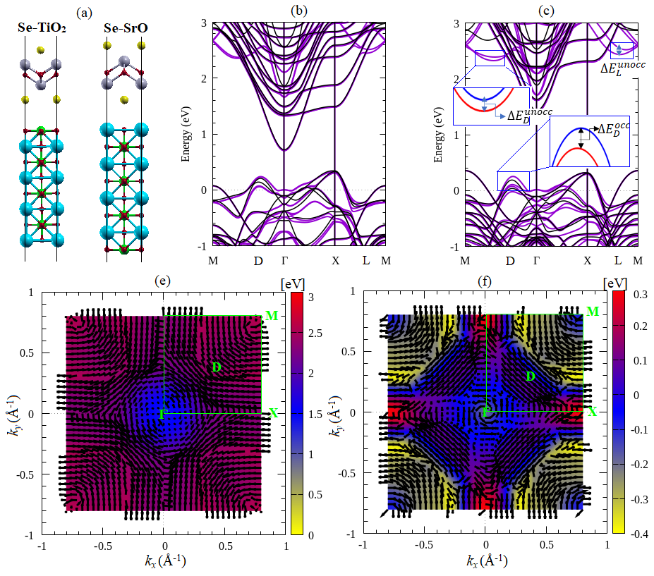
Finally, we explore the emergence of Rashba-spin-valley states in Bi2O2Se ML by considering a more realistic system. In this study, we propose an interfacial configuration consisting of a Bi2O2Se ML grown on a SrTiO3 [001] substrate. We investigate two different interface terminations, namely Se-SrO and Se-TiO2 terminations, as depicted in Figure 7(a). Both interface systems exhibit positive cohesive energies ( eV/Å2 and eV/Å2), indicating a thermodynamically stable binding between the Bi2O2Se ML and SrTiO3. Additional details, including the optimized interfacial lattice constant, interfacial distance, and interfacial charge transfer properties based on the average electrostatic potential, can be found in Table S1 and Fig. S2 in the supplementary materials [62]. Overall, our calculations confirm that the interfacial strength and stability of both interface systems are closely related to the bonding characteristics at the heterointerface.
Figs. 7(b)-7(c) show the electronic band structure of Bi2O2Se ML/SrTiO3 interface with Se-SrO and Se-TiO2 interface terminations calculated without (black) and with (red) including the SOC, respectively. Due to the defect contributor of the Bi2O2Se ML in the Bi2O2Se ML/SrTiO3 interface, several occupied states near the Fermi level are observed, resulting in semi-metallic features of the electronic states. We find that the occupied states mainly originated from the Se- mixing with Bi- states of the Bi2O2Se, while the unoccupied states are contributed mainly by the Ti- states with a small admixture of O- and Sr- states of SrTiO3, see Fig. S3 in the supplementary materials [62]. Importantly, we identify large spin splitting, which occurs around the and valleys as highlighted in Fig. 7(c). The calculated spin-splitting parameters (, , , , ) are listed in Table III for different interface terminations. Although these parameters are smaller than that of the Bi2O2Se ML, they are still comparable with that reported on various 2D materials listed in Table I. Moreover, these splittings exhibit highly persistent in-plane spin textures around the valley and the Rashba spin textures around the valley [see Figs. 7(d)-7(e)], indicating that the Rashba-spin-valley states is achieved similar to that observed on the Bi2O2Se ML. Due to a significant energy difference of approximately 0.22 eV between the valley and the valley in the highest occupied state, the dominance of in-plane persistent spin textures is expected to govern the spin-polarized states. This dominance serves as a protective mechanism against decoherence, facilitating non-dissipative spin transport. Given the experimental report by Liang et. al.[40] on the successful molecular beam epitaxy (MBE) growth of an atomically thin Bi2O2Se film with an ML structure on the SrTiO (001) substrate, it is expected that the observation of the Rashba-spin-valley states in the Bi2O2Se ML/SrTiO3 (001) system will soon be achievable.
IV Conclussion
In summary, based on first-principles DFT calculations supported by symmetry analysis, we have systematically investigated the SOC-related properties of the strained Bi2O2Se ML. Breaking the crystal inversion symmetry of 2D Bi2O2Se ML with an external electric field causes the formation of Rashba-spin-valley states, characterized by Rashba-type spin splitting around the valley and spin-valley coupling at valleys along the line. In contrast to the Rashba-spin-valley states widely studied on previously reported 2D materials [10, 14, 15, 16, 17, 18, 26, 27, 28, 29, 30, 31, 32], we observed persistent spin texture with in-plane orientation around the valleys, as well as conventional Rashba-type spin textures around the valley. The electric field-induced reduction of crystal symmetry from to point group is responsible for these spin textures, which is confirmed by a model derived from symmetry analysis. Importantly, manipulating the Rashba and spin-valley states through biaxial strain provides an effective route to control the spin textures and spin splitting, which prevents electron back-scattering, and hence significantly enhances the efficiency of the spin transport.
Since the Rashba-spin-valley states observed in the present study are solely enforced by the point group symmetry, it is expected that these states can also be achieved on other 2D materials having a similar point group symmetry. Recently, another layered bismuth oxychalcogenide has been experimentally reported, including Bi2O2Te [75] and Bi2O2S [76], which possess a similar crystal symmetry. Therefore, similar features of the Rashba-spin-valley states could be observed.
Finally, the potential of utilizing the Bi2O2Se ML in spintronics and valleytronics-based devices is emphasized by considering a practical system, specifically the Bi2O2Se ML/SrTiO3 (001) heterointerface. This system supports robust Rashba-spin-valley states, highlighting its relevance in realistic applications. Therefore, this prediction is expected to trigger further theoretical and experimental studies to clarify the emergence of the Rashba-spin-valley states in 2D-based bismuth oxychalcogenide systems, which would be useful for future spintronic and valleytronic applications.
Acknowledgements.
This work was supported by collaborative research project 2023 supported by the Faculty of Mathematics and Natural Sciences, Universitas Gadjah Mada, Indonesia. The computation in this research was performed using the computer facilities at Universitas Gadjah Mada, Indonesia.References
- Manchon et al. [2015] A. Manchon, H. C. Koo, J. Nitta, S. M. Frolov, and R. A. Duine, New perspectives for Rashba spin-orbit coupling, Nat. Mater. 14, 871 (2015).
- Schaibley et al. [2016] J. R. Schaibley, H. Yu, G. Clark, P. Rivera, J. S. Ross, K. L. Seyler, W. Yao, and X. Xu, Valleytronics in 2d materials, Nature Reviews Materials 1, 16055 (2016).
- Ahn [2020] E. C. Ahn, 2d materials for spintronic devices, npj 2D Materials and Applications 4, 17 (2020).
- Rashba [1960] E. I. Rashba, Properties of semiconductors with an extremum loop. 1. Cyclotron and combinational resonance in a magnetic field perpendicular to the plane of the loop, Sov. Phys. Solid State 2, 1224 (1960).
- Dresselhaus [1955] G. Dresselhaus, Spin-orbit coupling effects in zinc blende structures, Phys. Rev. 100, 580 (1955).
- Di Sante et al. [2012] D. Di Sante, P. Barone, R. Bertacco, and S. Picozzi, Electric control of the giant rashba effect in bulk gete, Advanced Materials 25, 509 (2012).
- Plekhanov et al. [2014] E. Plekhanov, P. Barone, D. Di Sante, and S. Picozzi, Engineering relativistic effects in ferroelectric snte, Phys. Rev. B 90, 161108 (2014).
- Kuhlen et al. [2012] S. Kuhlen, K. Schmalbuch, M. Hagedorn, P. Schlammes, M. Patt, M. Lepsa, G. Güntherodt, and B. Beschoten, Electric field-driven coherent spin reorientation of optically generated electron spin packets in InGaAs, Phys. Rev. Lett. 109, 146603 (2012).
- Datta and Das [1990] S. Datta and B. Das, Electronic analog of the electro‐optic modulator, Appl. Phys. Lett. 56, 665 (1990).
- Xiao et al. [2012] D. Xiao, G.-B. Liu, W. Feng, X. Xu, and W. Yao, Coupled spin and valley physics in monolayers of and other group-vi dichalcogenides, Phys. Rev. Lett. 108, 196802 (2012).
- Lu et al. [2013] H.-Z. Lu, W. Yao, D. Xiao, and S.-Q. Shen, Intervalley scattering and localization behaviors of spin-valley coupled dirac fermions, Phys. Rev. Lett. 110, 016806 (2013).
- Gunawan et al. [2006] O. Gunawan, Y. P. Shkolnikov, K. Vakili, T. Gokmen, E. P. De Poortere, and M. Shayegan, Valley susceptibility of an interacting two-dimensional electron system, Phys. Rev. Lett. 97, 186404 (2006).
- Rycerz et al. [2007] A. Rycerz, J. Tworzydło, and C. W. J. Beenakker, Valley filter and valley valve in graphene, Nature Physics 3, 172 (2007).
- Mak et al. [2014] K. F. Mak, K. L. McGill, J. Park, and P. L. McEuen, The valley hall effect in mos¡sub¿2¡/sub¿ transistors, Science 344, 1489 (2014).
- Onga et al. [2017] M. Onga, Y. Zhang, T. Ideue, and Y. Iwasa, Exciton hall effect in monolayer mos2, Nature Materials 16, 1193 (2017).
- Sheoran et al. [2023] S. Sheoran, S. Monga, A. Phutela, and S. Bhattacharya, Coupled spin-valley, rashba effect, and hidden spin polarization in wsi2n4 family, The Journal of Physical Chemistry Letters 14, 1494 (2023), pMID: 36745045.
- Yang et al. [2021] C. Yang, Z. Song, X. Sun, and J. Lu, Valley pseudospin in monolayer and , Phys. Rev. B 103, 035308 (2021).
- Zhou et al. [2021] W. Zhou, L. Wu, A. Li, B. Zhang, and F. Ouyang, Structural symmetry, spin–orbit coupling, and valley-related properties of monolayer wsi2n4 family, The Journal of Physical Chemistry Letters 12, 11622 (2021).
- Zeng et al. [2012] H. Zeng, J. Dai, W. Yao, D. Xiao, and X. Cui, Valley polarization in mos2 monolayers by optical pumping, Nature Nanotechnology 7, 490 (2012).
- Cao et al. [2012] T. Cao, G. Wang, W. Han, H. Ye, C. Zhu, J. Shi, Q. Niu, P. Tan, E. Wang, B. Liu, and J. Feng, Valley-selective circular dichroism of monolayer molybdenum disulphide, Nature Communications 3, 887 (2012).
- Wakatsuki et al. [2017] R. Wakatsuki, Y. Saito, S. Hoshino, Y. M. Itahashi, T. Ideue, M. Ezawa, Y. Iwasa, and N. Nagaosa, Nonreciprocal charge transport in noncentrosymmetric superconductors, Science Advances 3, e1602390 (2017).
- Dyakonov and Perel [1972] M. I. Dyakonov and V. I. Perel, . spin relaxation of conduction electrons in noncentrosymmetric semiconductors, Sov. Phys. Solid State 13, 3023 (1972).
- Araki et al. [2014] Y. Araki, G. Khalsa, and A. H. MacDonald, Weak localization, spin relaxation, and spin diffusion: Crossover between weak and strong rashba coupling limits, Phys. Rev. B 90, 125309 (2014).
- Liu et al. [2015] H. Liu, J. Chen, H. Yu, F. Yang, L. Jiao, G.-B. Liu, W. Ho, C. Gao, J. Jia, W. Yao, and M. Xie, Observation of intervalley quantum interference in epitaxial monolayer tungsten diselenide, Nature Communications 6, 8180 (2015).
- Yang et al. [2015] L. Yang, N. A. Sinitsyn, W. Chen, J. Yuan, J. Zhang, J. Lou, and S. Crooker, Long-lived nanosecond spin relaxation and spin coherence of electrons in monolayer mos2 and ws2, Nature Physics 11, 830 (2015).
- Yu et al. [2021] S.-B. Yu, M. Zhou, D. Zhang, and K. Chang, Spin hall effect in the monolayer janus compound mosse enhanced by rashba spin-orbit coupling, Phys. Rev. B 104, 075435 (2021).
- Absor et al. [2018] M. A. U. Absor, H. Kotaka, F. Ishii, and M. Saito, Tunable spin splitting and spin lifetime in polar wste monolayer, Japanese Journal of Applied Physics 57, 04FP01 (2018).
- Yao et al. [2017] Q.-F. Yao, J. Cai, W.-Y. Tong, S.-J. Gong, J.-Q. Wang, X. Wan, C.-G. Duan, and J. H. Chu, Manipulation of the large rashba spin splitting in polar two-dimensional transition-metal dichalcogenides, Phys. Rev. B 95, 165401 (2017).
- Rezavand et al. [2022] A. Rezavand, N. Ghobadi, and B. Behnamghader, Electronic and spintronic properties of janus ( = mo, w) monolayers, Phys. Rev. B 106, 035417 (2022).
- Hussain et al. [2022] G. Hussain, A. Samad, M. Ur Rehman, G. Cuono, and C. Autieri, Emergence of rashba splitting and spin-valley properties in janus mogesip2as2 and wgesip2as2 monolayers, Journal of Magnetism and Magnetic Materials 563, 169897 (2022).
- Wang et al. [2019a] Y. Wang, W. Wei, H. Wang, N. Mao, F. Li, B. Huang, and Y. Dai, Janus tixy monolayers with tunable berry curvature, The Journal of Physical Chemistry Letters 10, 7426 (2019a).
- Ahammed and De Sarkar [2022] R. Ahammed and A. De Sarkar, Valley spin polarization in two-dimensional monolayers: Merger of valleytronics with spintronics, Phys. Rev. B 105, 045426 (2022).
- Sheng et al. [2021] F. Sheng, C. Hua, M. Cheng, J. Hu, X. Sun, Q. Tao, H. Lu, Y. Lu, M. Zhong, K. Watanabe, T. Taniguchi, Q. Xia, Z.-A. Xu, and Y. Zheng, Rashba valleys and quantum hall states in few-layer black arsenic, Nature 593, 56 (2021).
- Meng et al. [2018] M. Meng, S. Huang, C. Tan, J. Wu, Y. Jing, H. Peng, and H. Q. Xu, Strong spin–orbit interaction and magnetotransport in semiconductor bi2o2se nanoplates, Nanoscale 10, 2704 (2018).
- Gao et al. [2022] J. Gao, F. Lu, X. Liu, J. Deng, X. Zhang, Z. Sun, X. Liu, X. Shi, N. Wang, Y. Wu, W. Wang, and X. Ding, Detection and tuning of spin-orbit interactions on inclined-grown bi2o2se nanoplates, Applied Physics Letters 120, 013105 (2022).
- Wu et al. [2017a] J. Wu, H. Yuan, M. Meng, C. Chen, Y. Sun, Z. Chen, W. Dang, C. Tan, Y. Liu, J. Yin, Y. Zhou, S. Huang, H. Q. Xu, Y. Cui, H. Y. Hwang, Z. Liu, Y. Chen, B. Yan, and H. Peng, High electron mobility and quantum oscillations in non-encapsulated ultrathin semiconducting bi2o2se, Nature Nanotechnology 12, 530 (2017a).
- Wu et al. [2017b] J. Wu, C. Tan, Z. Tan, Y. Liu, J. Yin, W. Dang, M. Wang, and H. Peng, Controlled synthesis of high-mobility atomically thin bismuth oxyselenide crystals, Nano Letters 17, 3021 (2017b).
- Chen et al. [2018] C. Chen, M. Wang, J. Wu, H. Fu, H. Yang, Z. Tian, T. Tu, H. Peng, Y. Sun, X. Xu, J. Jiang, N. B. M. Schröter, Y. Li, D. Pei, S. Liu, S. A. Ekahana, H. Yuan, J. Xue, G. Li, J. Jia, Z. Liu, B. Yan, H. Peng, and Y. Chen, Electronic structures and unusually robust bandgap in an ultrahigh-mobility layered oxide semiconductor, bi2o2se, Science Advances 4, eaat8355 (2018).
- Zhang et al. [2013] K. Zhang, C. Hu, X. Kang, S. Wang, Y. Xi, and H. Liu, Synthesis and thermoelectric properties of bi2o2se nanosheets, Materials Research Bulletin 48, 3968 (2013).
- Liang et al. [2019] Y. Liang, Y. Chen, Y. Sun, S. Xu, J. Wu, C. Tan, X. Xu, H. Yuan, L. Yang, Y. Chen, P. Gao, J. Guo, and H. Peng, Molecular beam epitaxy and electronic structure of atomically thin oxyselenide films, Advanced Materials 31, 1901964 (2019).
- Theurich and Hill [2001] G. Theurich and N. A. Hill, Self-consistent treatment of spin-orbit coupling in solids using relativistic fully separable ab initio pseudopotentials, Phys. Rev. B 64, 073106 (2001).
- Ozaki [2003] T. Ozaki, Variationally optimized atomic orbitals for large-scale electronic structures, Phys. Rev. B 67, 155108 (2003).
- Ozaki and Kino [2004] T. Ozaki and H. Kino, Numerical atomic basis orbitals from h to kr, Phys. Rev. B 69, 195113 (2004).
- Ozaki and Kino [2005] T. Ozaki and H. Kino, Efficient projector expansion for the ab initio lcao method, Phys. Rev. B 72, 045121 (2005).
- Perdew et al. [1996] J. P. Perdew, K. Burke, and M. Ernzerhof, Generalized gradient approximation made simple, Phys. Rev. Lett. 77, 3865 (1996).
- Kohn and Sham [1965] W. Kohn and L. J. Sham, Self-consistent equations including exchange and correlation effects, Phys. Rev. 140, A1133 (1965).
- Lejaeghere et al. [2016] K. Lejaeghere, G. Bihlmayer, T. Björkman, P. Blaha, S. Blügel, V. Blum, D. Caliste, I. E. Castelli, S. J. Clark, A. Dal Corso, S. de Gironcoli, T. Deutsch, J. K. Dewhurst, I. Di Marco, C. Draxl, M. Dułak, O. Eriksson, J. A. Flores-Livas, K. F. Garrity, L. Genovese, P. Giannozzi, M. Giantomassi, S. Goedecker, X. Gonze, O. Grånäs, E. K. U. Gross, A. Gulans, F. Gygi, D. R. Hamann, P. J. Hasnip, N. A. W. Holzwarth, D. Iuşan, D. B. Jochym, F. Jollet, D. Jones, G. Kresse, K. Koepernik, E. Küçükbenli, Y. O. Kvashnin, I. L. M. Locht, S. Lubeck, M. Marsman, N. Marzari, U. Nitzsche, L. Nordström, T. Ozaki, L. Paulatto, C. J. Pickard, W. Poelmans, M. I. J. Probert, K. Refson, M. Richter, G.-M. Rignanese, S. Saha, M. Scheffler, M. Schlipf, K. Schwarz, S. Sharma, F. Tavazza, P. Thunström, A. Tkatchenko, M. Torrent, D. Vanderbilt, M. J. van Setten, V. Van Speybroeck, J. M. Wills, J. R. Yates, G.-X. Zhang, and S. Cottenier, Reproducibility in density functional theory calculations of solids, Science 351, 10.1126/science.aad3000 (2016).
- Tadano and Tsuneyuki [2015] T. Tadano and S. Tsuneyuki, Self-consistent phonon calculations of lattice dynamical properties in cubic with first-principles anharmonic force constants, Phys. Rev. B 92, 054301 (2015).
- Kotaka et al. [2013] H. Kotaka, F. Ishii, and M. Saito, Rashba effect on the structure of the bi one-bilayer film: Fully relativistic first-principles calculation, Japanese Journal of Applied Physics 52, 035204 (2013).
- Yamaguchi and Ishii [2017] N. Yamaguchi and F. Ishii, Strain-induced large spin splitting and persistent spin helix at laalo3/srtio3 interface, Applied Physics Express 10, 123003 (2017).
- Absor and Ishii [2021] M. A. U. Absor and F. Ishii, Large band splitting with tunable spin polarization in the two-dimensional ferroelectric family (; ), Phys. Rev. B 103, 045119 (2021).
- Sasmito et al. [2021] S. A. Sasmito, M. Anshory, I. Jihad, and M. A. U. Absor, Reversible spin textures with giant spin splitting in two-dimensional (, te; , br, i) compounds for a persistent spin helix, Phys. Rev. B 104, 115145 (2021).
- Absor and Santoso [2022] M. A. U. Absor and I. Santoso, Reversible canted persistent spin textures in two-dimensional ferroelectric bilayer wte2, Journal of Applied Physics 132, 183906 (2022).
- Absor et al. [2022] M. A. U. Absor, A. Lukmantoro, and I. Santoso, Full-zone persistent spin textures with giant spin splitting in two-dimensional group iv–v compounds, Journal of Physics: Condensed Matter 34, 445501 (2022).
- Absor et al. [2021] M. A. U. Absor, Y. Faishal, M. Anshory, I. Santoso, Sholihun, Harsojo, and F. Ishii, Highly persistent spin textures with giant tunable spin splitting in the two-dimensional germanium monochalcogenides, Journal of Physics: Condensed Matter 33, 305501 (2021).
- Absor et al. [2020] M. A. U. Absor, I. Santoso, N. Yamaguchi, and F. Ishii, Spin splitting with persistent spin textures induced by the line defect in the phase of monolayer transition metal dichalcogenides, Phys. Rev. B 101, 155410 (2020).
- Liang et al. [2020] J. Liang, T. Tu, G. Chen, Y. Sun, R. Qiao, H. Ma, W. Yu, X. Zhou, C. Ma, P. Gao, H. Peng, K. Liu, and D. Yu, Unveiling the fine structural distortion of atomically thin bi2o2se by third-harmonic generation, Advanced Materials 32, 2002831 (2020), https://onlinelibrary.wiley.com/doi/pdf/10.1002/adma.202002831 .
- Zhang et al. [2020] Y. Zhang, Q. Gao, X. Han, and Y. Peng, Mechanical flexibility and strain engineered-band structures of monolayer bi2o2se, Physica E: Low-dimensional Systems and Nanostructures 116, 113728 (2020).
- Tang et al. [2021] H. Tang, B. Shi, Y. Wang, C. Yang, S. Liu, Y. Li, R. Quhe, and J. Lu, Layer-dependent photoabsorption and photovoltaic effects in two-dimensional (x = , , and ), Phys. Rev. Appl. 15, 064037 (2021).
- Wang et al. [2019b] N. Wang, M. Li, H. Xiao, H. Gong, Z. Liu, X. Zu, and L. Qiao, Optimizing the thermoelectric transport properties of bi2o2se monolayer via biaxial strain, Phys. Chem. Chem. Phys. 21, 15097 (2019b).
- Pang and Li [2021] Z. Pang and T. Li, Mechanics and strain engineering of bulk and monolayer bi2o2se, Journal of the Mechanics and Physics of Solids 157, 104626 (2021).
- [62] see Supplemental Material at [URL will be inserted by publisher] for the calculated results of phonon dispersion bands of the Bi2O2Se ML under the equilibrium conditions, the applied of biaxial strains, and external electric fields. The supllementary materials also includes the stability and electronic structures of Bi2O2Se ML/SrTiO3 [001]. .
- Wang et al. [2018] X.-P. Wang, X.-B. Li, N.-K. Chen, J.-H. Zhao, Q.-D. Chen, and H.-B. Sun, Electric field analyses on monolayer semiconductors: the example of inse, Phys. Chem. Chem. Phys. 20, 6945 (2018).
- Feng et al. [2021] X.-Q. Feng, H.-X. Lu, D.-N. Shi, J.-M. Jia, and C.-S. Wang, Semiconductor-metal transition induced by combined electric field and external strain in bilayer phosphorene, Solid State Communications 337, 114434 (2021).
- Schliemann et al. [2003] J. Schliemann, J. C. Egues, and D. Loss, Nonballistic spin-field-effect transistor, Phys. Rev. Lett. 90, 146801 (2003).
- Tao and Tsymbal [2018] L. L. Tao and E. Y. Tsymbal, Persistent spin texture enforced by symmetry, Nature Communications 9, 2763 (2018).
- Autieri et al. [2019] C. Autieri, P. Barone, J. Sławińska, and S. Picozzi, Persistent spin helix in rashba-dresselhaus ferroelectric , Phys. Rev. Materials 3, 084416 (2019).
- Bernevig et al. [2006] B. A. Bernevig, J. Orenstein, and S.-C. Zhang, Exact su(2) symmetry and persistent spin helix in a spin-orbit coupled system, Phys. Rev. Lett. 97, 236601 (2006).
- Altmann et al. [2014] P. Altmann, M. P. Walser, C. Reichl, W. Wegscheider, and G. Salis, Suppressed decay of a laterally confined persistent spin helix, Phys. Rev. B 90, 201306 (2014).
- Winkler et al. [2003] R. Winkler, S. Papadakis, E. De Poortere, and M. Shayegan, Spin-Orbit Coupling in Two-Dimensional Electron and Hole Systems (Springer, Berlin, 2003).
- Vajna et al. [2012] S. Vajna, E. Simon, A. Szilva, K. Palotas, B. Ujfalussy, and L. Szunyogh, Higher-order contributions to the rashba-bychkov effect with application to the bi/ag(111) surface alloy, Phys. Rev. B 85, 075404 (2012).
- Arras et al. [2019] R. Arras, J. Gosteau, H. J. Zhao, C. Paillard, Y. Yang, and L. Bellaiche, Rashba-like spin-orbit and strain effects in tetragonal , Phys. Rev. B 100, 174415 (2019).
- Anshory and Absor [2020] M. Anshory and M. A. U. Absor, Strain-controlled spin-splitting in the persistent spin helix state of two-dimensional snse monolayer, Physica E: Low-dimensional Systems and Nanostructures 124, 114372 (2020).
- Gomes and Carvalho [2015] L. C. Gomes and A. Carvalho, Phosphorene analogues: Isoelectronic two-dimensional group-iv monochalcogenides with orthorhombic structure, Phys. Rev. B 92, 085406 (2015).
- Ai et al. [2022] W. Ai, J. Chen, X. Dong, Z. Gao, Y. He, Z. Liu, H. Fu, F. Luo, and J. Wu, High mobility and quantum oscillations in semiconducting bi2o2te nanosheets grown by chemical vapor deposition, Nano Letters 22, 7659 (2022).
- Yang et al. [2022] X. Yang, L. Qu, F. Gao, Y. Hu, H. Yu, Y. Wang, M. Cui, Y. Zhang, Z. Fu, Y. Huang, W. Feng, B. Li, and P. Hu, High-performance broadband photoelectrochemical photodetectors based on ultrathin bi2o2s nanosheets, ACS Applied Materials & Interfaces 14, 7175 (2022).