Conductance oscillations of antiferromagnetic layer tunnel junctions
Abstract
We study conductance oscillations of antiferromagnetic layer tunnel junctions composed of antiferromagnetic topological insulators (MTIs) such as MnBi2Te4. In presence of an in-plane magnetic field, we find that the two terminal differential conductance across the junction oscillates as a function of field strength. Notably, the quantum interference at weak fields for the even-layer case is distinctive from the odd-layer case due to the scattering phase shift . Consequently, the differential conductance is vanishing (maximized) at integer magnetic flux quanta for even-layer (odd-layer) junctions. The conductance oscillations manifest the layer-dependent quantum interference in which symmetries and scattering phases play essential roles. In numerical calculations, we observe that the quantum interference undergoes an evolution from SQUID-like to Fraunhofer-like oscillations as the junction length increases.
I Introduction
Magnetism and topology are two main research areas of modern physics. Many efforts have been devoted to study the interplay of magnetism and topology in magnetic topological materials, for instance, in magnetic topological insulators [1, 2, 3, 4, 5, 6, 7]. The quantum anomalous Hall effect is one of the key features of magnetic topological insulators that can be employed in prototype quantum devices [8, 9, 10]. However, the working temperature of the quantum anomalous Hall effect is limited by the small surface gap and disorder in magnetically doped topological insulators. The recently discovered intrinsic magnetic topological insulator MnBi2Te4 gives hope for the observation of the quantum anomalous Hall effect at high temperatures [11, 12, 13]. It is a versatile material with rich topological physics [14, 15, 16, 17, 18, 19, 20, 21, 22], such as axion insulators [23, 24, 25, 26], higher Chern numbers [27] and type-II Weyl semimetals [28, 29].
In thin films of magnetic topological insulators, top and bottom surface states hybridize due to finite-size effects. Previous studies have shown that hybridization can be exploited to tune the properties of topological insulators, which can be utilized in prototype topological electronics [30, 31], especially in topological transistors [32, 33, 34, 35, 36, 37]. Recently, a new mechanism of magnetic topological transistors has been proposed based on the layer degree of freedom of MnBi2Te4 [38]. The magnetic topological transistor works well for even-layer thin films thanks to compensated magnetization, whereas hybridization hampers the performance in odd-layer thin films. Up to now, the influence of in-plane magnetic fields on the performance of magnetic topological transistors has not been analyzed. We show it in this work that magnetic fields substantially affect the transport characteristics of such devices.
To do so, we investigate the scattering processes of an antiferromagnetic layer tunnel junction (ALTJ) composed of intrinsic magnetic topological insulators MnBi2Te4 in presence of hybridization. The junction is formed between two regions with (anti-)parallel electric fields, applied perpendicularly to the layers of the magnetic topological insulators. We provide analytical results of the scattering matrices and the transmission probability for both odd- and even-layer junctions with and without in-plane magnetic fields. In absence of magnetic fields, quantum interference is constructive for the odd-layer case, while it is destructive for the even-layer case due to symmetry constraints. In presence of in-plane magnetic fields, the two terminal differential conductance oscillates as the magnetic field increases. The conductance oscillations manifest the layer-dependent quantum interference. We observe that this quantum interference undergoes an evolution from SQUID-like to Fraunhofer-like oscillations as the junction length increases. These features indicate particular quantum interference in ALTJs that allows us to observe characteristic properties of topological surface states.
This article is organized as follows. In Sec. II, we provide the effective surface model for intrinsic antiferromagnetic topological insulators MnBi2Te4 in presence of vertical electric fields and in-plane magnetic fields. We also describe the method used for numerical simulations. In Sec. III, we show the analytical results of the scattering matrix and transmission probability of ALTJs for both odd- and even-layer films. The transport results of ALTJs in presence of in-plane magnetic fields are presented in Sec. IV. We conclude in Sec. V.
II Model
We provide theoretical models which are used to calculate the conductance oscillations of ALTJs. In Sec. II.1, we present the low-energy effective Hamiltonian. In Sec. II.2, we introduce the theoretical formalism for the calculation of the two terminal electrical conductance.
II.1 Low-energy effective Hamiltonian
We begin with an effective model of antiferromagnetic MnBi2Te4 thin films in presence of out-of-plane electric fields and in-plane magnetic fields. MnBi2Te4 is a magnetic topological insulator with intrinsic antiferromagnetic order [23, 11, 39]. Out-of-plane electric fields can be realized by dual gates [26, 40]. We assume that the resulting electric potential is an odd function of without loss of generality. To derive the effective surface model, we project the bulk Hamiltonian onto the surface states of the topological insulator [41, 42, 18]. Thus, the effective surface model reads [38]
| (1) |
where describes the Dirac surface states of topological insulators given by
| (2) |
The Pauli matrices and act on top and bottom surface state and spin space, respectively. The basis of the model is , where and are the lowest-energy eigenstates of topological insulators at the point with spin . We consider the in-plane magnetic field with minimal coupling to a vector potential describing a magnetic field along the -axis, i.e., . The last term in Eq. (2) describes the overlap between top and bottom surface states with coupling strength , which is exponentially small for thick films. is the thickness of the MTI film. is the localization length of the surface states along the -axis. is a bulk parameter of the material MnBi2Te4. Both and are determined from parameter sets of MnBi2Te4 based on ab initio calculations [23].
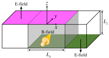
An ALTJ is formed between the regions with two electric fields [see Fig. 1], described by in Eq. (1),
| (3) |
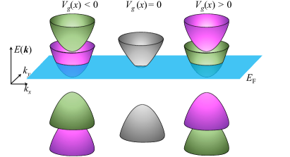
where is the effective electric potential acting on the surface states with being the strength of the gate potential. The magnetic junction is formed in the region with . The effective electric potential acting on the left (right) region of the junction is (). Hence, shifts top and bottom surface states in energy oppositely [38].
The last term in Eq. (1) describes the effective exchange field of the surface states. Due to the antiferromagnetic order in the bulk, the form of is layer number dependent. For odd-layer films, the directions of the effective exchange fields at top and bottom surfaces are the same, leading to
| (4) |
For even-layer films, the directions of the effective exchange fields at top and bottom surfaces are opposite, leading to
| (5) |
and are the strength of the corresponding effective exchange field [38].
II.2 Two terminal conductance
We employ the Landauer formalism to evaluate the two terminal electrical conductance [43, 44, 45].
| (6) |
where is the conductance quantum, is the Fermi distribution function. is the transmission probability from the left region to the right region (see Fig. 2). We obtain the differential conductance as at zero temperature, where is Fermi energy.
We calculate the transmission probability analytically for short junctions in Sec. III using the effective Hamiltonian of Eq. (1). In addition, we complement the analytical calculation with numerical calculation of for long junctions in Sec. IV. We conduct the numerical simulation considering the discretized 3D bulk Hamiltonian on a cubic lattice and exploiting the recursive Green function technique, where
| (7) |
Here, is the retarded Green function of the junction region, . and are the self-energies of the left and right regions, respectively. are the linewidth functions. is the advanced Green function.
III Transmission probability without a magnetic field
To reveal the physical origin for the conductance oscillations in presence of an in-plane magnetic field, we analyze the transmission probability in terms of the physical scattering processes without magnetic field first. Interestingly, we identify scattering processes involving distinct quantum interferences. We show that the quantum interference for odd- and even-layer films, respectively, occurs constructively and destructively due to particular symmetries between top and bottom layers. In Sec. III.1, we present the generic scattering processes. In Sec. III.2 and III.3, we provide analytical results of the transmission probability for odd- and even-layer ALTJs demonstrating the constructive and destructive interference.
We obtain analytical results of using the effective Hamiltonian Eq. (1). To simplify the analysis, we focus on the case that the Fermi energy is close to the band bottom of the junction region, . In this regime, is dominated by the transmission of electrons with perpendicular angle of incidence at the junction. Then, the scattering problem effectively becomes a one-dimensional scattering problem between top and bottom layers along the -axis.
III.1 Scattering matrices
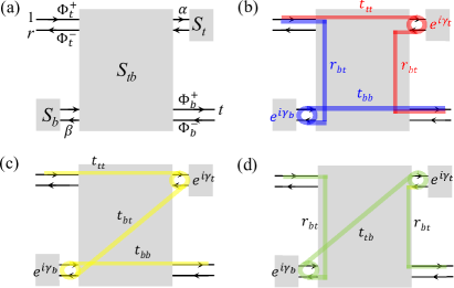
We now describe the scattering matrices , , and used to calculate (see Fig. 3). () is the scattering matrix of bottom (top) surface state in the left (right) region. As the gates deplete one of the surface states, the incident electrons in each case are fully reflected accumulating the phase factor (see Fig. 2 and Fig. 3). Meanwhile, in the junction region, both top and bottom surface states are filled up to the Fermi energy. We introduce to describe electron scattering in the junction region,
| (8) |
where .
We derive the transmission amplitude by combining the scattering matrices , , and ,
| (9) |
where are outgoing scattering amplitudes [see Fig. 3(a)]. The resulting transmission amplitude is
| (10) | |||||
where appears due to multiple phase accumulations at the top layer of the right region. occurs similarly at the bottom layer of the left region. For thick ALTJs, the denominators of second, third, and fourth terms can be approximated by , since higher orders of the scattering between top and bottom layers are negligibly small for thick layers. The second term in Eq.(10) corresponds to the scattering processes illustrated in Fig. 3(b), involving (flux-dependent) quantum interference. The third and fourth terms correspond to those illustrated in Figs. 3(c) and 3(d), respectively.
III.2 Transmission through odd-layer junctions
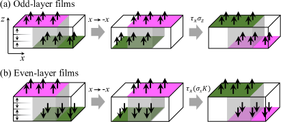
We show that the inversion symmetry of ALTJs of odd-layer films results in constructive quantum interference. We begin with providing the scattering matrix for odd-layer films:
| (11) |
where , , , and due to inversion symmetry [see Fig. 4(a)]. Hence, we can simplify the transmission amplitude in Eq. (10) for odd-layer films as
| (12) |
where scattering processes are kept up to the second order of the amplitudes , , , and to focus on the dominating ones [Derivations of , , , and are provided in Appendix A]. We note that the second term in Eq. (12) is responsible for quantum interference.
Moreover, we identify that the inversion symmetry of ALTJs of odd-layer films results in constructive quantum interference at zero magnetic field. The scattering phase in Eq. (12) can be written as
| (13) |
The value of alone depends on various parameters such as Fermi energy , gate voltage , and effective magnetization at the surface . However, we find that the difference of the phases and vanishes owing to inversion symmetry, resulting in constructive quantum interference.
III.3 Transmission through even-layer junctions
Due to the antiferromagnetic ordering across the layers of ALTJs, the transmission of even-layer films shows distinct features from odd-layer films [see Fig. 4]. We show that the particular type of the inversion symmetry of even-layer films, followed by spin inversion, results in destructive quantum interference for the transmission probability.
From the particular inversion symmetry of even-layer films, we find that the transmission between top and bottom layer are prohibited . This is because spin-flip tunneling between top and bottom layers is blocked. Hence, only the scattering process shown in Fig. 3(b) is responsible for the transmission in even-layer films. The transmission amplitude for even-layer films becomes
| (14) |
where all orders of scattering processes are kept. The scattering matrix for even-layer films is given by
| (15) |
where and . [Matrix elements of are provided in Appendix A.]
While the scattering phase is again the one in Eq. (13), we find that the particular inversion symmetry of even-layer films enforces . Hence, the quantum interference of the ALTJ of even-layer films is destructive with . We note that the scattering phase shift stems from the geometric phase associated with topological junctions [46].
IV Conductance oscillations due to in-plane magnetic fields
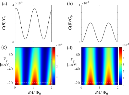
We study conductance oscillations of ALTJs in presence of in-plane magnetic fields . First, we evaluate analytically using the effective Hamiltonian Eq. (1) and analyze the relevant scattering processes in Sec.IV.1. The analytical results show that the conductance oscillations of odd-layer junctions are maximized at integer magnetic flux quanta. In contrast, we identify that for even-layer junctions is shifted by the half magnetic flux quantum due to the scattering phase difference . Second, we provide numerical results of the conductance oscillations for various lengths in Sec. IV.2. Interestingly, we find that the conductance oscillations exhibit a crossover from SQUID-like to Fraunhofer-like behavior as the length of the junction increases.
IV.1 Analytical calculations for short junctions
We obtain the conductance oscillations from the transmission at a given Fermi energy . We note that various scattering paths in the junction region accumulate different quantum phases from the in-plane magnetic field. For short junctions , the dynamical phase is substantially smaller than the Peierl’s phase of the magnetic field. We consider thick films for which higher orders of interlayer scattering are negligible. We take the magnetic field into account as phase shifts of the scattering matrix for a given gauge choice,
| (16) |
with , the in-plane area of the junction, and the magnetic flux quantum. We attribute the conductance oscillations to quantum interference. Note that the scattering processes shown in Fig. 3(b) dominate the transmission across the junction.
We first show that conductance oscillations for the odd-layer case as a function of magnetic field [Figs. 5(a) and (c)]. Unfortunately, the transmission probability for the odd-layer case does not allow a simple expression. However, we provide an approximated solution for odd-layer case in the leading order of interlayer scattering and as
| (17) | |||
where . The transmission probability of the odd-layer case is approximately reduced to the numerator of the first term . Accordingly, is maximized at integer multiples of magnetic flux quanta.
We now present for the even-layer case [Figs. 5(b) and (d)]. It can understood by the analytical result of the transmission probability
| (18) |
where , , , and . Due to the scattering phase shift , the conductance oscillation of the even-layer junctions is shifted by half the magnetic flux quantum from of the odd-layer case. Hence, the conductance oscillates as the magnetic field increases and vanishes at integer multiples of magnetic flux quanta.
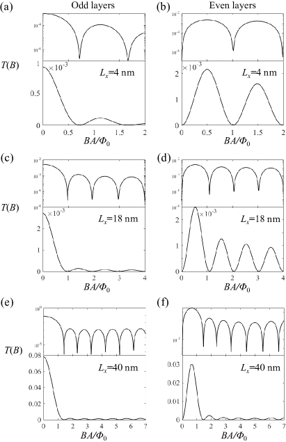
IV.2 Numerical calculations for short and long junctions
The conductance oscillations of short ALTJs in Sec. IV.1 require strong magnetic fields due to the small lateral cross section of short junctions. To overcome this limitation, we numerically study the conductance oscillations for various junction lengths in this section.
For short junctions of odd-layer films, we find the numerically obtained conductance oscillation shows qualitatively similar behaviors to the analytical result in Sec. IV.1 in that is maximized around the integer multiples of magnetic flux quanta [Fig. 6(a)]. However, the visibility of the numerically obtained decreases fast as increasing magnetic fields . This is because the numerical calculation includes more realistic scattering paths forming various interference loops enclosing smaller magnetic flux quanta than analytical calculations. On the other hand, the numerically obtained conductance oscillation for even-layer films exhibits more similar behaviors to the analytical results in Sec. IV.1 with vanishing at the integer multiples of magnetic flux quanta but with the much slower decaying visibility. We attribute the slower decaying visibility of even-layer junctions to the fact that only the scattering processes in Fig. 3(b) are responsible for the conductance oscillation of even-layer junctions, while all scattering processes in Fig. 3 contribute to of odd-layer junctions. Hence, when we focus on the visibilities, the analytical calculations for even-layer films becomes more consistent with realistic numerical calculations than that for the odd-layer films. However, we highlight that the overall oscillatory behaviors of analytical and numerical calculation exhibit the same results, when we focus on the magnetic flux quanta maximizing and minimizing .
For long junctions at high magnetic fields, the accumulated quantum phases of different scattering paths can vary significantly [Figs. 6(e) and (f)], beyond the scope of the analytical method. We find that the various scattering paths for the conductance oscillations result in Fraunhofer-like interference patterns. Figs. 6(c) and (d) show intermediate junction lengths with SQUID-like [Figs. 6(a) and (b)] and Fraunhofer-like oscillation patterns [Figs. 6(e) and (f)]. However, for weak magnetic fields , the quantum interferences for the even- and odd-layer junctions remain the same regardless of the length of junctions. For the even-layer case, it becomes finite from zero and oscillates as the magnetic field increases. For the odd-layer case, the conductance peak is reduced due to the presence of the in-plane magnetic field.
V Conclusion
To summarize, we study the scattering processes of an antiferromagnetic layer tunnel junction composed of intrinsic magnetic topological insulators MnBi2Te4 in presence of hybridization. We obtain analytical results of the scattering matrices and the transmission probabilities for both odd- and even-layer junctions with and without in- plane magnetic fields. We show that the two paths of most dominating scattering processes at first order of the small scattering between top and bottom layers form a quantum interference loop enclosing a magnetic flux in presence of in-plane magnetic fields. Importantly, we reveal that the scattering processes involving distinct quantum interference in odd- and even-layer films at weak fields are constructive and destructive, respectively, due to their particular symmetries. Thus, the differential conductance is vanishing (maximized) at integer magnetic flux quanta for even-layer (odd-layer) junctions. Additionally, we observe that the quantum interference undergoes an evolution from SQUID-like to Fraunhofer-like oscillations as the junction length increases. It indicates that for a long ALTJ various scattering paths in the junction region get involved. These features imply rich quantum interference in ALTJs that makes the observation of characteristic properties of topological surface states in ALTJs possible.
Acknowledgements.
This work was supported by the Würzburg-Dresden Cluster of Excellence on Complexity and Topology in Quantum Matter (EXC2147, project-id 390858490) and by the DFG (SFB1170 “ToCoTronics”). We thank the Bavarian Ministry of Economic Affairs, Regional Development and Energy for financial support within the High-Tech Agenda Project “Bausteine für das Quanten Computing auf Basis topologischer Materialen”.Appendix A Derivation of the scattering matrix
We adopt a matrix approach for the wavefunction matching method, which yields the scattering matrices . Since top and bottom surface states in the junction region are degenerate, four wavefunctions are provided to be matched with incoming and outgoing scattering states at and . The wavefunction matching can be written in a matrix form as
| (23) | |||
| where | |||
| (26) | |||
| (29) |
is a matrix whose elements form linear combinations of wavefunctions in the junction region. If we are only interested in the scattering matrix, the precise form of is irrelevant. Our matrix approach yields the scattering matrix as
| (30) |
We apply the matrix approach to the derivation of the scattering matrix of odd layers. The scattering amplitudes of are obtained as
| (31) | |||||
| (32) | |||||
| (33) | |||||
| (34) |
with . In addition, the scattering amplitudes of for even-layers are obtained as
| (35) | |||||
| (36) | |||||
| (37) |
with .
References
- Liu et al. [2016] C.-X. Liu, S.-C. Zhang, and X.-L. Qi, The Quantum Anomalous Hall Effect: Theory and Experiment, Annual Review of Condensed Matter Physics 7, 301 (2016).
- Tokura et al. [2019] Y. Tokura, K. Yasuda, and A. Tsukazaki, Magnetic topological insulators, Nat. Rev. Phys. 1, 126 (2019).
- Wang et al. [2021] P. Wang, J. Ge, J. Li, Y. Liu, Y. Xu, and J. Wang, Intrinsic magnetic topological insulators, Innovation 2 (2021).
- Bernevig et al. [2022] B. A. Bernevig, C. Felser, and H. Beidenkopf, Progress and prospects in magnetic topological materials, Nature 603, 41 (2022).
- Chang et al. [2023] C.-Z. Chang, C.-X. Liu, and A. H. MacDonald, Colloquium: Quantum anomalous Hall effect, Rev. Mod. Phys. 95, 011002 (2023).
- Wang et al. [2023] Y. Wang, X.-M. Ma, Z. Hao, Y. Cai, H. Rong, F. Zhang, W. Chen, C. Zhang, J. Lin, Y. Zhao, C. Liu, Q. Liu, and C. Chen, On the topological surface states of the intrinsic magnetic topological insulator Mn-Bi-Te family, National Science Review , nwad066 (2023).
- Li et al. [2023] S. Li, T. Liu, C. Liu, Y. Wang, H.-Z. Lu, and X. C. Xie, Progress on antiferromagnetic topological insulator MnBi2Te4, National Science Review , nwac296 (2023).
- He et al. [2014] K. He, Y. Wang, and Q.-K. Xue, Quantum anomalous Hall effect, National Science Review 1, 38 (2014).
- Bhattacharyya et al. [2021] S. Bhattacharyya, G. Akhgar, M. Gebert, J. Karel, M. T. Edmonds, and M. S. Fuhrer, Recent Progress in Proximity Coupling of Magnetism to Topological Insulators, Advanced Materials 33, 2007795 (2021).
- Chi and Moodera [2022] H. Chi and J. S. Moodera, Progress and prospects in the quantum anomalous Hall effect, APL Materials 10, 090903 (2022).
- Otrokov et al. [2019a] M. M. Otrokov, I. I. Klimovskikh, H. Bentmann, D. Estyunin, A. Zeugner, Z. S. Aliev, S. Gaß, A. U. B. Wolter, A. V. Koroleva, A. M. Shikin, M. Blanco-Rey, M. Hoffmann, I. P. Rusinov, A. Y. Vyazovskaya, S. V. Eremeev, Y. M. Koroteev, V. M. Kuznetsov, F. Freyse, J. Sánchez-Barriga, I. R. Amiraslanov, M. B. Babanly, N. T. Mamedov, N. A. Abdullayev, V. N. Zverev, A. Alfonsov, V. Kataev, B. Büchner, E. F. Schwier, S. Kumar, A. Kimura, L. Petaccia, G. Di Santo, R. C. Vidal, S. Schatz, K. Kißner, M. Ünzelmann, C. H. Min, S. Moser, T. R. F. Peixoto, F. Reinert, A. Ernst, P. M. Echenique, A. Isaeva, and E. V. Chulkov, Prediction and observation of an antiferromagnetic topological insulator, Nature 576, 416 (2019a).
- Deng et al. [2020] Y. Deng, Y. Yu, M. Z. Shi, Z. Guo, Z. Xu, J. Wang, X. H. Chen, and Y. Zhang, Quantum anomalous Hall effect in intrinsic magnetic topological insulator MnBi2Te4, Science 367, 895 (2020).
- Deng et al. [2021] H. Deng, Z. Chen, A. Wołoś, M. Konczykowski, K. Sobczak, J. Sitnicka, I. V. Fedorchenko, J. Borysiuk, T. Heider, Ł. Pluciński, K. Park, A. B. Georgescu, J. Cano, and L. Krusin-Elbaum, High-temperature quantum anomalous Hall regime in a MnBi2Te4/Bi2Te3 superlattice, Nat. Phys. 17, 36 (2021).
- Li et al. [2019a] J. Li, Y. Li, S. Du, Z. Wang, B.-L. Gu, S.-C. Zhang, K. He, W. Duan, and Y. Xu, Intrinsic magnetic topological insulators in van der Waals layered MnBi2Te4-family materials, Sci. Adv. 5, eaaw5685 (2019a).
- Li et al. [2019b] H. Li, S.-Y. Gao, S.-F. Duan, Y.-F. Xu, K.-J. Zhu, S.-J. Tian, J.-C. Gao, W.-H. Fan, Z.-C. Rao, J.-R. Huang, J.-J. Li, D.-Y. Yan, Z.-T. Liu, W.-L. Liu, Y.-B. Huang, Y.-L. Li, Y. Liu, G.-B. Zhang, P. Zhang, T. Kondo, S. Shin, H.-C. Lei, Y.-G. Shi, W.-T. Zhang, H.-M. Weng, T. Qian, and H. Ding, Dirac Surface States in Intrinsic Magnetic Topological Insulators EuSn2As2 and MnBi2nTe3n+1, Phys. Rev. X 9, 041039 (2019b).
- Hao et al. [2019] Y.-J. Hao, P. Liu, Y. Feng, X.-M. Ma, E. F. Schwier, M. Arita, S. Kumar, C. Hu, R. Lu, M. Zeng, Y. Wang, Z. Hao, H.-Y. Sun, K. Zhang, J. Mei, N. Ni, L. Wu, K. Shimada, C. Chen, Q. Liu, and C. Liu, Gapless Surface Dirac Cone in Antiferromagnetic Topological Insulator MnBi2Te4, Phys. Rev. X 9, 041038 (2019).
- Zhang et al. [2020] R.-X. Zhang, F. Wu, and S. Das Sarma, Möbius Insulator and Higher-Order Topology in MnBi2nTe3n+1, Phys. Rev. Lett. 124, 136407 (2020).
- Sun et al. [2020] H.-P. Sun, C. M. Wang, S.-B. Zhang, R. Chen, Y. Zhao, C. Liu, Q. Liu, C. Chen, H.-Z. Lu, and X. C. Xie, Analytical solution for the surface states of the antiferromagnetic topological insulator MnBi2Te4, Phys. Rev. B 102, 241406 (2020).
- Wu et al. [2020] X. Wu, J. Li, X.-M. Ma, Y. Zhang, Y. Liu, C.-S. Zhou, J. Shao, Q. Wang, Y.-J. Hao, Y. Feng, E. F. Schwier, S. Kumar, H. Sun, P. Liu, K. Shimada, K. Miyamoto, T. Okuda, K. Wang, M. Xie, C. Chen, Q. Liu, C. Liu, and Y. Zhao, Distinct Topological Surface States on the Two Terminations of MnBi4Te7, Phys. Rev. X 10, 031013 (2020).
- Yang et al. [2021] S. Yang, X. Xu, Y. Zhu, R. Niu, C. Xu, Y. Peng, X. Cheng, X. Jia, Y. Huang, X. Xu, J. Lu, and Y. Ye, Odd-Even Layer-Number Effect and Layer-Dependent Magnetic Phase Diagrams in MnBi2Te4, Phys. Rev. X 11, 011003 (2021).
- Li et al. [2021] H. Li, H. Jiang, C.-Z. Chen, and X. C. Xie, Critical Behavior and Universal Signature of an Axion Insulator State, Phys. Rev. Lett. 126, 156601 (2021).
- Chen et al. [2023] R. Chen, H.-P. Sun, and B. Zhou, Side-surface-mediated hybridization in axion insulators, Phys. Rev. B 107, 125304 (2023).
- Zhang et al. [2019] D. Zhang, M. Shi, T. Zhu, D. Xing, H. Zhang, and J. Wang, Topological Axion States in the Magnetic Insulator MnBi2Te4 with the Quantized Magnetoelectric Effect, Phys. Rev. Lett. 122, 206401 (2019).
- Otrokov et al. [2019b] M. M. Otrokov, I. P. Rusinov, M. Blanco-Rey, M. Hoffmann, A. Yu. Vyazovskaya, S. V. Eremeev, A. Ernst, P. M. Echenique, A. Arnau, and E. V. Chulkov, Unique Thickness-Dependent Properties of the van der Waals Interlayer Antiferromagnet MnBi2Te4 Films, Phys. Rev. Lett. 122, 107202 (2019b).
- Liu et al. [2020] C. Liu, Y. Wang, H. Li, Y. Wu, Y. Li, J. Li, K. He, Y. Xu, J. Zhang, and Y. Wang, Robust axion insulator and Chern insulator phases in a two-dimensional antiferromagnetic topological insulator, Nat. Mater. 19, 522 (2020).
- Gao et al. [2021] A. Gao, Y.-F. Liu, C. Hu, J.-X. Qiu, C. Tzschaschel, B. Ghosh, S.-C. Ho, D. Bérubé, R. Chen, H. Sun, Z. Zhang, X.-Y. Zhang, Y.-X. Wang, N. Wang, Z. Huang, C. Felser, A. Agarwal, T. Ding, H.-J. Tien, A. Akey, J. Gardener, B. Singh, K. Watanabe, T. Taniguchi, K. S. Burch, D. C. Bell, B. B. Zhou, W. Gao, H.-Z. Lu, A. Bansil, H. Lin, T.-R. Chang, L. Fu, Q. Ma, N. Ni, and S.-Y. Xu, Layer Hall effect in a 2D topological axion antiferromagnet, Nature 595, 521 (2021).
- Ge et al. [2020] J. Ge, Y. Liu, J. Li, H. Li, T. Luo, Y. Wu, Y. Xu, and J. Wang, High-Chern-number and high-temperature quantum Hall effect without Landau levels, Natl. Sci. Rev. 7, 1280 (2020).
- Lee et al. [2021] S. H. Lee, D. Graf, L. Min, Y. Zhu, H. Yi, S. Ciocys, Y. Wang, E. S. Choi, R. Basnet, A. Fereidouni, A. Wegner, Y.-F. Zhao, K. Verlinde, J. He, R. Redwing, V. Gopalan, H. O. H. Churchill, A. Lanzara, N. Samarth, C.-Z. Chang, J. Hu, and Z. Q. Mao, Evidence for a Magnetic-Field-Induced Ideal Type-II Weyl State in Antiferromagnetic Topological Insulator Mn(Bi1-xSbx)2Te4, Phys. Rev. X 11, 031032 (2021).
- Lei et al. [2022] X. Lei, L. Zhou, Z. Hao, H. Liu, S. Yang, H. Sun, X. Ma, C. Ma, L. Wang, H.-Z. Lu, J.-W. Mei, J. Wang, and H. He, Magnetically tunable Shubnikov–de Haas oscillations in MnBi2Te4, Phys. Rev. B 105, 155402 (2022).
- Xu et al. [2019] Y. Xu, G. Jiang, I. Miotkowski, R. R. Biswas, and Y. P. Chen, Tuning Insulator-Semimetal Transitions in 3D Topological Insulator thin Films by Intersurface Hybridization and In-Plane Magnetic Fields, Phys. Rev. Lett. 123, 207701 (2019).
- Chong et al. [2022] S. K. Chong, L. Liu, K. Watanabe, T. Taniguchi, T. D. Sparks, F. Liu, and V. V. Deshpande, Emergent helical edge states in a hybridized three-dimensional topological insulator, Nat Commun 13, 6386 (2022).
- Michetti and Trauzettel [2013] P. Michetti and B. Trauzettel, Devices with electrically tunable topological insulating phases, Appl. Phys. Lett. 102, 063503 (2013).
- Qian et al. [2014] X. Qian, J. Liu, L. Fu, and J. Li, Quantum spin Hall effect in two-dimensional transition metal dichalcogenides, Science 346, 1344 (2014).
- Liu et al. [2014] J. Liu, T. H. Hsieh, P. Wei, W. Duan, J. Moodera, and L. Fu, Spin-filtered edge states with an electrically tunable gap in a two-dimensional topological crystalline insulator, Nat. Mater. 13, 178 (2014).
- Wang et al. [2015] J. Wang, B. Lian, and S.-C. Zhang, Electrically Tunable Magnetism in Magnetic Topological Insulators, Phys. Rev. Lett. 115, 036805 (2015).
- Liu et al. [2015] Q. Liu, X. Zhang, L. B. Abdalla, A. Fazzio, and A. Zunger, Switching a Normal Insulator into a Topological Insulator via Electric Field with Application to Phosphorene, Nano Lett. 15, 1222 (2015).
- Collins et al. [2018] J. L. Collins, A. Tadich, W. Wu, L. C. Gomes, J. N. B. Rodrigues, C. Liu, J. Hellerstedt, H. Ryu, S. Tang, S.-K. Mo, S. Adam, S. A. Yang, M. S. Fuhrer, and M. T. Edmonds, Electric-field-tuned topological phase transition in ultrathin Na3Bi, Nature 564, 390 (2018).
- Sun et al. [2023] H.-P. Sun, C.-A. Li, S.-J. Choi, S.-B. Zhang, H.-Z. Lu, and B. Trauzettel, Magnetic topological transistor exploiting layer-selective transport, Phys. Rev. Res. 5, 013179 (2023).
- Gong et al. [2019] Y. Gong, J. Guo, J. Li, K. Zhu, M. Liao, X. Liu, Q. Zhang, L. Gu, L. Tang, X. Feng, D. Zhang, W. Li, C. Song, L. Wang, P. Yu, X. Chen, Y. Wang, H. Yao, W. Duan, Y. Xu, S.-C. Zhang, X. Ma, Q.-K. Xue, and K. He, Experimental Realization of an Intrinsic Magnetic Topological Insulator, Chinese Phys. Lett. 36, 076801 (2019).
- Cai et al. [2022] J. Cai, D. Ovchinnikov, Z. Fei, M. He, T. Song, Z. Lin, C. Wang, D. Cobden, J.-H. Chu, Y.-T. Cui, C.-Z. Chang, D. Xiao, J. Yan, and X. Xu, Electric control of a canted-antiferromagnetic Chern insulator, Nat. Commun. 13, 1668 (2022).
- Lu et al. [2010] H.-Z. Lu, W.-Y. Shan, W. Yao, Q. Niu, and S.-Q. Shen, Massive Dirac fermions and spin physics in an ultrathin film of topological insulator, Phys. Rev. B 81, 115407 (2010).
- Shan et al. [2010] W.-Y. Shan, H.-Z. Lu, and S.-Q. Shen, Effective continuous model for surface states and thin films of three-dimensional topological insulators, New J. Phys. 12, 043048 (2010).
- Landauer [1970] R. Landauer, Electrical resistance of disordered one-dimensional lattices, The Philosophical Magazine 21, 863 (1970).
- Büttiker [1986] M. Büttiker, Four-Terminal Phase-Coherent Conductance, Phys. Rev. Lett. 57, 1761 (1986).
- Datta [1997] S. Datta, Electronic Transport in Mesoscopic Systems (Cambridge University Press, 1997).
- Choi et al. [2013] S.-J. Choi, S. Park, and H.-S. Sim, Tunable geometric phase of dirac fermions in a topological junction, Phys. Rev. B 87, 165420 (2013).