Theory of the microwave impedance microscopy of Chern insulators
Abstract
Microwave impedance microscopy (MIM) has been utilized to directly visualize topological edge states in many quantum materials, from quantum Hall systems to topological insulators, across the GHz regime. While the microwave response for conventional metals and insulators can be accurately quantified using simple lumped-element circuits, the applicability of these classical models to more exotic quantum systems remains limited. In this work, we present a general theoretical framework of the MIM response of arbitrary quantum materials within linear response theory. As a special case, we model the microwave response of topological edge states in a Chern insulator and predict an enhanced MIM response at the crystal boundaries due to collective edge magnetoplasmon (EMP) excitations. The resonance frequency of these plasmonic modes should depend quantitatively on the topological invariant of the Chern insulator state and on the sample’s circumference, which highlights their non-local, topological nature. To benchmark our analytical predictions, we experimentally probe the MIM response of quantum anomalous Hall edge states in a \ceCr-doped \ce(Bi,Sb)2Te3 topological insulator and perform numerical simulations using a classical formulation of the EMP modes based on this realistic tip-sample geometry, both of which yield results consistent with our theoretical picture. We also show how the technique of MIM can be used to quantitatively extract the topological invariant of a Chern insulator, disentangle the signatures of topological versus trivial edge states, and shed light on the microscopic nature of dissipation along the crystal boundaries.
I Introduction
Chern insulators host chiral one-dimensional edge states and exhibit a quantized Hall conductance due to a non-trivial topological band structure. The experimental signatures of Chern insulators have been observed in a variety of material systems, from the quantum Hall family to magnetic topological insulators, and more recently moiré materials [1, 2, 3, 4, 5, 6, 7, 8, 9, 10]. A key feature of Chern insulators is the presence of topological edge modes, which are electronic states that propagate unidirectionally along the edges of the material without backscattering. While edge states in Chern insulators have been investigated extensively using electronic transport techniques[11, 12, 13, 14], these methods lack the spatial resolution to probe the detailed structure and the degree of localization of these modes.
To address this limitation, several imaging techniques have been used to directly visualize topological edge modes, including scanning tunneling microscopy (STM) [15, 16, 17, 18, 19], superconducting quantum interference device (SQUID) microscopy [20, 21, 22], as well as some interferometry techniques [23]. These experiments have detected current flow and an enhancement of the density of states at the boundaries of topological insulators, which have been interpreted as evidence for one-dimensional topological edge modes. However, this interpretation can be complicated by the presence of trivial electronic states at the physical boundaries arising from impurities, dangling bonds, and band bending [24, 25, 26].
In recent years, a near-field imaging technique called scanning microwave impedance microscopy (MIM) has shown great potential for spatially-resolved detection of topological boundary modes. Experiments have reported an enhanced microwave response at the edges of two-dimensional topological insulators and quantum Hall systems [27, 28, 29, 30, 24, 31], but the observed behavior cannot be easily explained by a simple conductance increase close to the edge using classical lumped-circuit models. Furthermore, the observed width of quantum Hall edge states, as measured by MIM, is an order of magnitude larger than that measured by transport and STM, significantly exceeding the magnetic length [32, 33, 34, 15, 16, 17, 18, 19, 35, 36]. This motivates our development of a theoretical foundation to compute the microwave response of quantum materials that cannot simply be characterized by a scalar conductivity value.
In this paper, we develop a general theoretical framework that quantifies the MIM response of a quantum material within linear response theory. Upon applying this theory to the special case of quantum anomalous Hall (QAH) insulators, we predict that an enhanced MIM response at the edge should arise from collective edge magnetoplasmon (EMP) modes that circulate along the sample boundary[37, 38, 39, 40, 41, 42, 43, 44]. The resonance frequency of these plasmonic modes should depend quantitatively on the topological invariant of the Chern insulator state and on the length of the sample’s perimeter [40, 37, 38, 39]. This non-trivial frequency dependence can unambiguously relate the enhanced edge signal observed with MIM to the one-dimensional topological edge modes that propagate around the entire sample perimeter, whereas topologically trivial edge effects are expected to be featureless in the frequency domain.
To check the validity of this analytical model, we experimentally measured the real-space MIM response of the QAH edge modes in a \ceCr-doped \ce(Bi,Sb)2Te3 magnetic topological insulator at various microwave frequencies and also conducted numerical simulations based on this experimental tip-sample setup, both of which yielded results consistent with the theoretical framework proposed here.
II Theory of the MIM response of quantum materials
MIM characterizes a material’s electronic response to microwave frequency electromagnetic fields confined to a small spatial region around a sharp metallic probe. In practice, a microwave excitation is coupled to an AFM tip in close proximity to the sample, and the real and imaginary parts of the reflected signals are measured using GHz lock-in detection techniques [45, 46, 47].
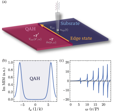
We first review the basics of the MIM measurement setup and then present a general model of the MIM response of quantum materials within linear response theory. As shown in Fig. 1, the MIM probe, driven by an AC voltage at microwave frequency, is brought near the sample surface. Unlike scanning tunneling microscopy (STM), the probe is only capacitively coupled to the sample. MIM measures the displacement current exchanged between the probe and the sample. This displacement current can be formally written as , where is the driven voltage and is the complex tip-sample admittance [45].
In practice, an impedance matching network is always necessary to maximize the sensitivity of the admittance measurement. Since is much smaller than the self-admittance of the MIM probe , the MIM signals are linearly proportional to the change in . Explicitly [45],
| (1) |
where is a real constant and is a complex constant. In the following section, we will show how to obtain in terms of the density response function of the system.
II.1 General framework
The most commonly used model of is the lumped-element model, which treats the sample as a resistor and a capacitor in parallel, then coupled capacitively to the tip [47]. This model can accurately predict the MIM response of conventional metals, dielectrics, and certain two-dimensional materials [46]. However, a more general theoretical framework is required to properly quantify the microwave response of more complex quantum materials, such as topological states of matter, that cannot be simply described by a pair of scalar conductivity and permittivity values. For example, in the case of QAH insulators, the model must accommodate one-dimensional gapless plasmon modes at the sample edge, which is outside the scope of the traditional lumped element picture.
We start by approximating the tip apex by a single point at and ignoring the rest of the tip (see Fig. 1). This approximation is well justified for shielded tips and qualitative sound for other type of metallic probes. Then the external potential generated by the tip is given by , where is the external charge at the apex of the tip, and is the Coulomb interaction inside the dielectric environment, which can either be calculated numerically, or be approximated by the vacuum value when contacts are sufficiently far away and capping layers are sufficiently thin. Now we write down the induced charge density in the sample in terms of the density response function,
| (2) |
with and both inside the sample. We will drop the index below to simplify the notation. This induced charge density in turn generates a potential at the apex of tip. The total potential at the peak of tip has an additional term due to the tip head capacitance , , then we can find the tip–sample admittance by expanding to the leading order in ,
| (3) |
We note that all constant terms and prefactors will be absorbed in the constants and in Eqn. (1) during impedance matching and therefore neglected from now on. Eqn. (3) is one of the main results of this work, which characterizes the MIM response of arbitrary quantum systems with describing the dynamical charge density-density correlation between and in the sample. The derivation of this equation uses only two assumptions: the tip can be approximated by a single point, and the microwave frequency electromagnetic field generated by MIM can be treated within linear response theory. The first assumption will be verified in a special case through numerical simulations in Sec. III, while the second assumption is supported by the high sensitivity of MIM provided by impedance matching.
Before we proceed to apply this general framework to Chern insulators, we will make a few comments on the result presented in Eqn. (3). First, this general result reduces to the lumped element model in the case of a simple homogeneous metal sheet with dielectric function ,
| (4) |
where is the sample thickness, is the tip–sample distance, and is the effective dielectric constant. approaches to the usual DC dielectric constant in the limit when the tip is sufficiently far from the sample. The lumped element model parameters are given by sample resistance , sample capacitance . The tip–sample capacitance that only shows up in constant terms and prefactors (see Ref. 47 Sec. SI for definitions and a full derivation).
Secondly, in the limit when the tip is sufficiently far from the sample, we can further approximate by ; then the MIM signal can be related to the electronic compressibility as follows:
| (5) |
where is the electron density and is the chemical potential. This provides a direct correspondence between the imaginary part of the MIM response and the chemical potential (which for example can be measured by scanning single-electron transistors and related field penetration techniques [48, 49]).
Finally, due to the factor of in Eqn. (3), the imaginary part of the MIM response, , comes from the real part of the density response function, , and vice versa. Thus, and measure the reflectivity and absorption of the sample, respectively.
II.2 Special case: Application to QAH insulators
To illustrate a concrete example, we now apply this general framework to calculate the MIM response of topological edge modes in a QAH insulator. The recipe is to first find all low energy excitations, then compute these excitations’ contribution to the density response function , and finally apply Eqn. (3) to find the MIM response. In two-dimensional QAH insulators, the bulk contributes little to the dielectric response because of the large energy gap, so we only need to focus on the edge contribution. The edge states in QAH insulators are characterized by the chiral Luttinger liquid that host plasmonic excitations [50, 44, 37]. These gapless edge plasmons modes are called edge magnetoplasmons (EMP) in the context of quantum Hall insulators and have been studied extensively for several decades [37, 38, 39, 41, 42, 43, 44]. More recently, they have also been studied in the context of QAH insulators [40], quantum spin Hall insulators [51] and Chern insulators [42]. To fully understand EMP modes beyond the chiral Luttinger liquid, prior theory work has also considered semiclassical corrections [41, 43, 37, 42].
In addition to EMP modes, edge acoustic modes have also been observed in the low energy excitation spectrum in QAH insulators [52, 53]. However, these modes are overdamped at microwave frequencies in the parameter regime of QAH insulators. Therefore, we can safely conclude that the MIM response in QAH insulators is dominated by edge plasmon modes. This is the underlying reason why the MIM response of a QAH insulator behaves so differently from the response of materials in which electron-hole pair excitation dominates. It might be a bit surprising since plasmon modes are usually not expected to show up in MIM data due to their finite energy gap. However, in QAH insulators these EMP modes are gapless due to the 1D nature of the edge states. In the following, we will only focus on the EMP contribution to .
If we place the tip a linear distance from the edge, the tip-sample admittance reduces to
| (6) |
where is the 1D momentum along the edge, is the sample perimeter, and is the 1D Fourier transform of the Coulomb interaction with being the modified Bessel function. In Ref. 47 Sec. SII, we compute for chiral edge modes at the RPA level,
| (7) |
where is the edge velocity and is the localization length of the edge mode, which is inversely proportional to the bulk gap and is assumed to be small compared to in Eqn. (6). In pure QAH samples where the Dirac velocity is the only energy scale, we expect . The poles of define the EMP frequencies,
| (8) |
This result agrees with Ref. [37], where the first term is referred to as the quantum part, and the second term is referred to as the classical part. The imaginary part of can be obtained by taking , then with being the delta function. In the experiment, could be a small but finite number due to dissipation effects, then would become a Lorentzian function centered at (see Ref. 47 Sec. SIII.1). Therefore, we expect the lineshape of the EMP resonance peaks to be broadened in the presence of dissipation along the sample boundaries. These features should allow microwave imaging to shed light on the the microscopic nature of the dissipation in the chiral edge modes, as revealed by the MIM response in the frequency domain.
Since we are operating at microwave frequencies, we have to worry about the quantization of momentum with being an integer, given the finite sample diameter . If the MIM frequency is comparable to the lowest few EMP resonances, the dominant contribution to the MIM response comes from a particular momentum whose EMP frequency is closest to , then
| (9) |
In experiments, we expect the case to hold given the size of the system [40].
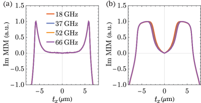
The presence of edge magnetoplasmons should be manifested experimentally in a strong enhancement of the MIM response at the boundaries of the QAH insulator, in agreement with prior experimental results [29, 30]. Fig. 1 (b) shows the spatial profile of the MIM response () of a QAH edge mode, revealing a sharp peak at the crystal boundaries, following Eqn. (9). The width of this edge peak is given by a characteristic length scale , the EMP wavelength, which can be as large as a few microns for realistic sample dimensions. It is generally expected that the edge width measured with MIM will be larger than the actual edge localization length due to long range Coulomb coupling between the tip and the sample. This observation helps explain the vastly different edge state widths reported in transport [32, 33] and STM [15, 16, 17, 18, 19] studies versus MIM experiments [29, 30].
Investigating the frequency dependence of the MIM edge peak should shed light on the topological nature of the Chern insulator state. Fig. 1 (c) illustrates the evolution of the edge peak amplitide as a function of the MIM excitation frequency . Here we plot as a function of for a fixed tip location over the sample edge, with , , and . The EMP resonances appear at a series of discrete microwave frequencies, which are found to depend quantitatively on both the topological invariant and the sample perimeter (see Ref. 47 Sec. SI) [40, 37, 38, 39]. Because trivial edge states localized at crystal boundaries should be featureless as a function of frequency, this unique fingerprint of the EMP resonances in the frequency domain provides a route to unambiguously differentiate between topological and trivial edge modes. The quantitative relationship between the resonance frequency and the sample circumference also illustrates non-local, topological nature of the chiral edge modes that circulate around the entire sample.
In practice, because continuously sweeping the MIM frequency can be experimentally challenging, one could first identify the EMP resonances using traditional microwave transmission measurements [40] and then perform MIM imagining at a few frequencies close to and away from those EMP resonances.
III Semiclassical simulations
To verify our analytical results, which were derived using an approximation that treats the MIM tip as a point, we also perform a numerical simulation of the MIM signal that incorporates a realistic tip-sample geometry and dielectric environment that had been neglected in the analytical treatment. The simulation still focuses on the topological edge state contribution to the MIM signal and utilizes a classical formulation of the EMP modes, which accurately capture the density response of these modes even though it may not accurately reproduce the EMP frequencies [41, 42]. This formulation requires solving Maxwell’s equations with a non-zero Hall conductance inside the sample, which therefore only captures the classical part of the EMP frequencies in Eqn. (8).
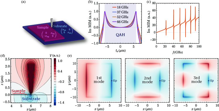
To compute the admittance , we use finite element analysis to numerically solve Maxwell’s equations for the entire experimental setup, including the MIM tip, the sample, and the substrate, as illustrated schematically in Fig. 2 (a) (see Ref. 47 Sec. SIII for details). The sample is placed on top of the substrate as in the experiment [29], which results in a step across the sample boundary (Fig. 2 (a)). The dielectric environment is set to be identical to the experiment setup, and the conductivity tensor is set to be inside the sample and zero outside. To ensure numerical convergence, we set the sample size to , which is much smaller than the one used in the experiment in Ref. 29 and Sec. IV. A side effect of scaling down the sample dimension is that we need to look at much higher frequencies in order to compare with the experiment since the first few EMP frequencies are scaled up the same time (see Eqn. (8) and Ref. 47 Sec. SIII.2 for details). More quantitatively, the first few EMP frequencies are about times larger than one would expect in the sample to be discussed in Sec. IV given their difference in perimeter. The topological nature of the problem requires a careful choice of the solver to ensure convergence [47].
Fig. 2 (b) displays a real-space plot of as the tip is scanned across the sample, which reproduces clear peaks at the sample boundaries, . The spatial profile of these edge peaks, including the decay length inside the sample, agree quantitatively with the analytical predictions in Fig. 1 (b). The most obvious difference lies in the asymmetry of inside and outside the sample in the simulation, which comes from the step and a change in dielectric environment across the sample boundary.
In Fig. 2 (b), we note that the spatially-resolved MIM signal is plotted at a series of generic frequencies, which are typically away from exact resonance frequencies. Upon analyzing the frequency dependence of , we find the edge peak to be narrower at higher frequencies. This phenomenon has a simple explanation within our theoretical framework. From Eqn. (8), we know that a higher frequency corresponds to a larger EMP momentum . Meanwhile, sets the decay length scale of the MIM signal when the tip moves away from the edge (see Eqn. (9)). Combining these two observations, the peak is expected to be narrower at higher frequencies at which the MIM response comes from a higher frequency EMP mode associated with a shorter decay length. This prediction will later be compared with experiments in the following section.
When the tip is positioned over the sample edge, the imaginary part of picks up a series of resonance peaks corresponding to the first few EMP modes (Fig. 2 (c)), in agreement with analytical predictions. However, compared to Fig. 1 (b), there is an additional contribution from the dielectric environment that scales linearly with the MIM frequency. Another noticeable feature is the absence of a zero frequency peak due to the factor of in Eqn. (9). In Ref. 47 Sec. SIV, we extract the dispersion of the EMP modes by identifying resonance peaks in , which agrees quantitatively well with the classical part of Eqn. (8).
Fig. 2 (d-e) illustrates the electric potential distribution in the plane of the sample at the first few EMP frequencies, which provides a visualization of the real-space charge density oscillations at the fundamental EMP mode and higher harmonics. As shown in Fig. 2 (e), when the MIM frequency coincides with these EMP resonance frequencies, positive and negative charges start to concentrate at the sample edge with an in-plane distribution , where is the distance along the edge, is the distance from the edge. We note that the phase is pinned by the location of the tip since the energy is minimized when the charge distribution is most negative beneath the tip. The characteristic potential distribution of standing wave patterns clearly identifies their plasmonic nature, while also confirming that the experimental setup is able to excite EMP modes. In Fig. 2 (d), we see that the potential starts to decay immediately away from the edge, suggesting that charges are spatially confined to the boundaries of the sample.
Finally, we comment on the how expected MIM signatures of the EMP modes in a QAH insulator can be distinguished from the signatures of trivial edge modes arising from impurities at the boundaries of a conventional insulator. As shown in Ref. 47 Sec. SIV, the peak conductance required to reproduce the shape of the MIM curve is as high as , which would require a large concentration of metallic impurities that are extremely unlikely given the current fabrication process. Additionally, the peak in the MIM response at the boundaries of the sample is found to vanish at magnetic fields corresponding to the phase, which suggests that the enhanced edge conduction not trivial in nature[29]. Meanwhile, in the trivial case, the profile of the MIM edge peak would remain the same across a large range of frequencies, in contrast to the expected MIM response from EMP modes based on the theoretical picture presented above.
IV Experimental results
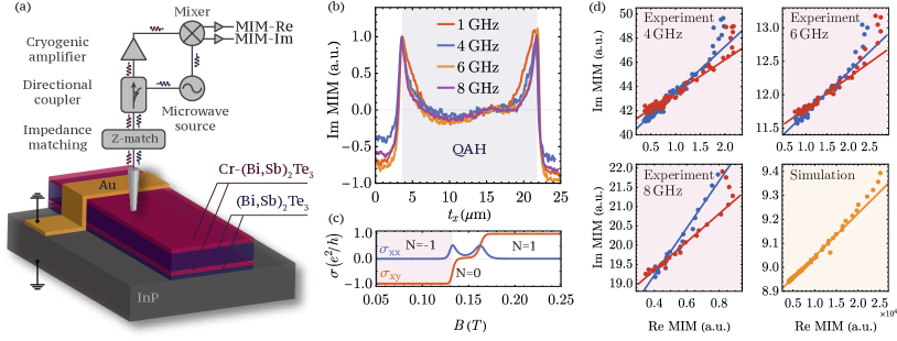
To verify our theoretical framework, we performed real-space microwave imaging of one-dimensional QAH edge states in a high-quality magnetic topological insulator thin film at various frequencies. The experimental setup is shown in Fig. 3 (a). The sample is a \ceCr-doped \ce(Bi,Sb)2Te3 Hall bar with dimensions of by , and we scan the MIM tip across the device parallel to the short edge. Details on device preparation and the MIM measurement setup can be found in Ref. 47 Sec. SVI. Transport measurements are used for a baseline characterization of the quality of the QAH insulator state. As shown in Fig. 3 (c), the Hall conductance is fully quantized and the longitudinal conductance drops to zero at below the coercive field, suggesting that current is primarily transmitted by chiral edge modes that are topologically protected from backscattering in the QAH phases (labeled by Chern number ).
The presence of the QAH edge modes is manifested experimentally in a sharp enhancement of the MIM response at the boundaries of the sample, as shown in the spatially-resolved microwave imaging data presented in Fig. 3 (b). (We remind readers that the experiment and the numerical simulations were performed at very different frequencies to compensate the difference in sample dimensions, but the resulting MIM data can still be compared at a qualitative level.)
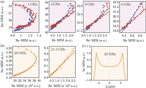
These experimental results have a few surprising features that differ from the expected behavior of a conventional insulator with an enhanced edge conductivity with trivial origins. First of all, the observed MIM signal is much stronger than that expected from edge defects or local doping (see Ref. 47 Sec. SIV for a comparison). If the MIM signal comes from the EMP modes, however, it is expected to diverge at EMP frequencies and can therefore be large in general. Another feature is that the real part of the measured MIM response is much smaller than the imaginary part, as shown in Fig. 3 (d). This can be explained by Eqn. (7) since is tiny except when the MIM frequency precisely hits one of the EMP frequencies. In addition, the spatial profile of the MIM response near the sample edge becomes narrower at a higher frequencies, which agrees qualitatively with the numerical simulations (see Fig. 3 (b) and Fig. 2 (b)).
Finally, we also investigate the relationship between the real and imaginary parts of the MIM response, measured as a function of position, at various frequencies. As shown in Fig. 3 (d), we note that the real and imaginary parts of the observed MIM response have a linear relation at frequencies higher than . This linear relationship provides strong evidence in favor of EMP modes being responsible for the enhanced MIM signal at the sample edge, and stands in sharp contrast to the expected semi-circle relation predicted by the lumped-element model. The results suggest that the MIM signal mainly comes from a 1D edge, then the dependence of and has to be the same. At frequencies lower than the first EMP resonance, the interpretation is complicated by the dielectric background. We refer interested readers to Ref. 47 Sec. SV for more details.
V Discussion and Outlook
This paper provides the first quantitative interpretation of the MIM response of quantum materials within linear response theory. In the limit when the tip is sufficiently far from the sample, we show that the imaginary part of the MIM response can be quantitatively related to the electronic compressibility. We would like to take this opportunity to compare MIM and the scanning SET technique, which directly measures chemical potential and therefore the electronic compressibility[48, 49]. MIM has the advantage of being less constrained by the electrostatic gating setup (and the associated fringing fields near the sample boundaries) and has a higher spatial resolution due to a simpler tip geometry, while scanning SET has the benefit of providing a more quantitative measurement of gap sizes and electronic compressibility without the need for impedance matching.
To illustrate a concrete application of the general model above, we compute the MIM response of a QAH insulator and reveal that the experimentally observed enhancement of the MIM signal at the sample boundaries comes from topological edge magnetoplasmon modes. This observation allows one to experimentally distinguish topologically nontrivial from trivial edge modes by investigating the quantitative relationship between the real and imaginary parts of the complex MIM response at multiple frequencies. Furthermore, this theoretical picture also allows us to predict the width of the experimentally observed peak of in MIM response at the boundaries of Chern insulators, which explains the apparent inconsistencies between the edge state decay length scales measured using MIM versus STM or transport[28, 31, 34, 35, 36].
To confirm and expand on the analytical results, we performed numerical simulations that took into account the effects of the tip-sample geometry and the dielectric background: the former turned out to be a small correction and the later only added linearly to the MIM signal. We also performed MIM measurements of the Chern insulator states in a \ceCr-doped \ce(Bi,Sb)2Te3 magnetic topological insulator at multiple frequencies to verify our theoretical understanding. We observed a clear peak in the MIM response at the edge of the sample, whose spatial profile, frequency dependence, and ratio of the real and imaginary parts of the MIM signal were consistent with our framework. We would like to point out that future MIM experiments with continuous frequency tunability would be desirable to fully verify our EMP interpretation of the MIM edge response in QAH insulators.

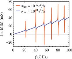
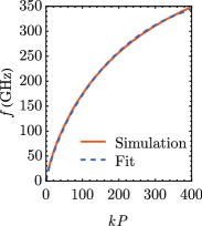
Finally, we would like to comment on our new formulation’s predictions for measuring the topological invariant of a Chern insulator using the technique of MIM. Expanding upon our previous calculations for QAH insulators with Chern number , the resonance frequency and MIM response can also be computed for systems with higher Chern numbers by including multiple branches in the density response calculation. At classical level, we expect both the EMP frequencies and the MIM signal magnitude right on the resonance to be linearly proportional to the Chern number as shown in Fig. 4, . We refer readers to Ref. 47 Eqn. (S27) for the full analytical formula with quantum corrections. We also expect the lineshape of the MIM signal to depend on the dissipation along the chiral edge states (manifested in a finite ), as discussed in Section II. These features should allow the technique of MIM to shed light on the Chern number of a topological state, as well as the microscopic nature of the dissipation at the sample boundaries.
Acknowledgements.
We thank Allan H. MacDonald, Tarun Grover, Yongtao Cui, Rahul Roy, Massoud R. Masir, Yahya Alavirad and Adrian B. Culver for inspiring discussions. We thank Alex Cauchon for helping develop some of the numerical simulations. M.T.A acknowledges funding support from the UC Office of the President, specifically the UC Laboratory Fees Research Program (award LFR-20-653926) and the AFOSR Young Investigator Program (award FA9550-20-1-0035). T.W. is supported by the U.S. Department of Energy, Office of Science, Office of Basic Energy Sciences, Materials Sciences and Engineering Division under Contract No. DE-AC02-05-CH11231 (Theory of Materials program KC2301). This work was partly supported by Japan Science and Technology Agency Core Research for Evolutional Science and Technology (JPMJCR16F1). Y.Z.Y. is supported by the NSF Grant DMR-2238360. Microwave impedance microscopy measurements at Stanford University were supported by the Gordon and Betty Moore Foundation’s Emergent Phenomena in Quantum Systems initiative through Grant GBMF4546 (Z.-X.S.) and by the National Science Foundation through Grant DMR-1305731.References
- von Klitzing [2017] K. von Klitzing, Quantum hall effect: Discovery and application, Annual Review of Condensed Matter Physics 8, 13 (2017).
- [2] C. Dean, P. Kim, J. I. A. Li, and A. Young, Fractional quantum hall effects in graphene, in Fractional Quantum Hall Effects, Chap. Chapter 7, pp. 317–375.
- Liu et al. [2016] C.-X. Liu, S.-C. Zhang, and X.-L. Qi, The quantum anomalous hall effect: Theory and experiment, Annual Review of Condensed Matter Physics 7, 301 (2016).
- He et al. [2018] K. He, Y. Wang, and Q.-K. Xue, Topological materials: Quantum anomalous hall system, Annual Review of Condensed Matter Physics 9, 329 (2018).
- Deng et al. [2020] Y. Deng, Y. Yu, M. Z. Shi, Z. Guo, Z. Xu, J. Wang, X. H. Chen, and Y. Zhang, Quantum anomalous hall effect in intrinsic magnetic topological insulator mnbi2te4, Science 367, 895 (2020).
- Sharpe et al. [2019] A. L. Sharpe, E. J. Fox, A. W. Barnard, J. Finney, K. Watanabe, T. Taniguchi, M. A. Kastner, and D. Goldhaber-Gordon, Emergent ferromagnetism near three-quarters filling in twisted bilayer graphene, Science 365, 605 (2019).
- Serlin et al. [2020] M. Serlin, C. L. Tschirhart, H. Polshyn, Y. Zhang, J. Zhu, K. Watanabe, T. Taniguchi, L. Balents, and A. F. Young, Intrinsic quantized anomalous hall effect in a moiré heterostructure, Science 367, 900 (2020).
- He et al. [2021] M. He, Y.-H. Zhang, Y. Li, Z. Fei, K. Watanabe, T. Taniguchi, X. Xu, and M. Yankowitz, Competing correlated states and abundant orbital magnetism in twisted monolayer-bilayer graphene, Nature Communications 12, 4727 (2021).
- Chen et al. [2020] G. Chen, A. L. Sharpe, E. J. Fox, Y.-H. Zhang, S. Wang, L. Jiang, B. Lyu, H. Li, K. Watanabe, T. Taniguchi, Z. Shi, T. Senthil, D. Goldhaber-Gordon, Y. Zhang, and F. Wang, Tunable correlated chern insulator and ferromagnetism in a moiré superlattice, Nature 579, 56 (2020).
- Wang et al. [2020] L. Wang, E.-M. Shih, A. Ghiotto, L. Xian, D. A. Rhodes, C. Tan, M. Claassen, D. M. Kennes, Y. Bai, B. Kim, K. Watanabe, T. Taniguchi, X. Zhu, J. Hone, A. Rubio, A. N. Pasupathy, and C. R. Dean, Correlated electronic phases in twisted bilayer transition metal dichalcogenides, Nature Materials 19, 861 (2020).
- Kouwenhoven et al. [1990] L. P. Kouwenhoven, B. J. van Wees, N. C. van der Vaart, C. J. P. M. Harmans, C. E. Timmering, and C. T. Foxon, Selective population and detection of edge channels in the fractional quantum hall regime, Phys. Rev. Lett. 64, 685 (1990).
- van Wees et al. [1989] B. J. van Wees, E. M. M. Willems, C. J. P. M. Harmans, C. W. J. Beenakker, H. van Houten, J. G. Williamson, C. T. Foxon, and J. J. Harris, Anomalous integer quantum hall effect in the ballistic regime with quantum point contacts, Phys. Rev. Lett. 62, 1181 (1989).
- Büttiker [1988] M. Büttiker, Absence of backscattering in the quantum hall effect in multiprobe conductors, Phys. Rev. B 38, 9375 (1988).
- Sabo et al. [2017] R. Sabo, I. Gurman, A. Rosenblatt, F. Lafont, D. Banitt, J. Park, M. Heiblum, Y. Gefen, V. Umansky, and D. Mahalu, Edge reconstruction in fractional quantum hall states, Nature Physics 13, 491 (2017).
- Howard et al. [2021] S. Howard, L. Jiao, Z. Wang, N. Morali, R. Batabyal, P. Kumar-Nag, N. Avraham, H. Beidenkopf, P. Vir, E. Liu, C. Shekhar, C. Felser, T. Hughes, and V. Madhavan, Evidence for one-dimensional chiral edge states in a magnetic weyl semimetal co3sn2s2, Nature Communications 12, 4269 (2021).
- Xu et al. [2022] H.-K. Xu, M. Gu, F. Fei, Y.-S. Gu, D. Liu, Q.-Y. Yu, S.-S. Xue, X.-H. Ning, B. Chen, H. Xie, Z. Zhu, D. Guan, S. Wang, Y. Li, C. Liu, Q. Liu, F. Song, H. Zheng, and J. Jia, Observation of magnetism-induced topological edge state in antiferromagnetic topological insulator mnbi4te7, ACS Nano 16, 9810 (2022).
- Lüpke et al. [2022] F. Lüpke, A. D. Pham, Y.-F. Zhao, L.-J. Zhou, W. Lu, E. Briggs, J. Bernholc, M. Kolmer, J. Teeter, W. Ko, C.-Z. Chang, P. Ganesh, and A.-P. Li, Local manifestations of thickness-dependent topology and edge states in the topological magnet , Phys. Rev. B 105, 035423 (2022).
- Zhang et al. [2022] C. Zhang, T. Zhu, S. Kahn, T. Soejima, K. Watanabe, T. Taniguchi, A. Zettl, F. Wang, M. P. Zaletel, and M. F. Crommie, Visualizing and manipulating chiral edge states in a moiré quantum anomalous hall insulator (2022), arXiv:2212.03380 .
- Tang et al. [2017] S. Tang, C. Zhang, D. Wong, Z. Pedramrazi, H.-Z. Tsai, C. Jia, B. Moritz, M. Claassen, H. Ryu, S. Kahn, J. Jiang, H. Yan, M. Hashimoto, D. Lu, R. G. Moore, C.-C. Hwang, C. Hwang, Z. Hussain, Y. Chen, M. M. Ugeda, Z. Liu, X. Xie, T. P. Devereaux, M. F. Crommie, S.-K. Mo, and Z.-X. Shen, Quantum spin hall state in monolayer 1t’-wte2, Nature Physics 13, 683 (2017).
- Spanton et al. [2014] E. M. Spanton, K. C. Nowack, L. Du, G. Sullivan, R.-R. Du, and K. A. Moler, Images of edge current in quantum wells, Phys. Rev. Lett. 113, 026804 (2014).
- Nichele et al. [2016] F. Nichele, H. J. Suominen, M. Kjaergaard, C. M. Marcus, E. Sajadi, J. A. Folk, F. Qu, A. J. A. Beukman, F. K. de Vries, and J. van Veen, Edge transport in the trivial phase of , New J. Phys. 18, 083005 (2016).
- Nowack et al. [2013] K. C. Nowack, E. M. Spanton, M. Baenninger, M. König, J. R. Kirtley, G. Kalisky, C. Ames, P. Leubner, C. Brüne, H. Buhmann, L. W. Molenkamp, D. Goldhaber-Gordon, and K. A. Moler, Imaging currents in quantum wells in the quantum spin hall regime, Nature Mater. 12, 787 (2013).
- Allen et al. [2016] M. T. Allen, O. Shtanko, I. C. Fulga, A. R. Akhmerov, K. Watanabe, T. Taniguchi, P. Jarillo-Herrero, L. S. Levitov, and A. Yacoby, Spatially resolved edge currents and guided-wave electronic states in graphene, Nature Phys. 12, 128 (2016).
- Ma et al. [2015] E. Y. Ma, M. R. Calvo, J. Wang, B. Lian, M. Mühlbauer, C. Brüne, Y.-T. Cui, K. Lai, W. Kundhikanjana, Y. Yang, M. Baenninger, M. König, C. Ames, H. Buhmann, P. Leubner, L. W. Molenkamp, S.-C. Zhang, D. Goldhaber-Gordon, M. A. Kelly, and Z.-X. Shen, Unexpected edge conduction in mercury telluride quantum wells under broken time-reversal symmetry, Nature Communications 6, 7252 (2015).
- Chang et al. [2015] C.-Z. Chang, W. Zhao, D. Y. Kim, P. Wei, J. K. Jain, C. Liu, M. H. W. Chan, and J. S. Moodera, Zero-field dissipationless chiral edge transport and the nature of dissipation in the quantum anomalous hall state, Phys. Rev. Lett. 115, 057206 (2015).
- Kou et al. [2014] X. Kou, S.-T. Guo, Y. Fan, L. Pan, M. Lang, Y. Jiang, Q. Shao, T. Nie, K. Murata, J. Tang, Y. Wang, L. He, T.-K. Lee, W.-L. Lee, and K. L. Wang, Scale-invariant quantum anomalous hall effect in magnetic topological insulators beyond the two-dimensional limit, Phys. Rev. Lett. 113, 137201 (2014).
- Shi et al. [2019] Y. Shi, J. Kahn, B. Niu, Z. Fei, B. Sun, X. Cai, B. A. Francisco, D. Wu, Z.-X. Shen, X. Xu, D. H. Cobden, and Y.-T. Cui, Imaging quantum spin hall edges in monolayer wte2, Science Advances 5, 10.1126/sciadv.aat8799 (2019).
- Lai et al. [2011] K. Lai, W. Kundhikanjana, M. A. Kelly, Z.-X. Shen, J. Shabani, and M. Shayegan, Imaging of coulomb-driven quantum hall edge states, Phys. Rev. Lett. 107, 176809 (2011).
- Allen et al. [2019] M. Allen, Y. Cui, E. Yue Ma, M. Mogi, M. Kawamura, I. C. Fulga, D. Goldhaber-Gordon, Y. Tokura, and Z.-X. Shen, Visualization of an axion insulating state at the transition between 2 chiral quantum anomalous hall states, Proceedings of the National Academy of Sciences 116, 14511 (2019).
- Lin et al. [2022] W. Lin, Y. Feng, Y. Wang, J. Zhu, Z. Lian, H. Zhang, H. Li, Y. Wu, C. Liu, Y. Wang, J. Zhang, Y. Wang, C.-Z. Chen, X. Zhou, and J. Shen, Direct visualization of edge state in even-layer mnbi2te4 at zero magnetic field, Nature Communications 13, 7714 (2022).
- Cui et al. [2016a] Y.-T. Cui, B. Wen, E. Y. Ma, G. Diankov, Z. Han, F. Amet, T. Taniguchi, K. Watanabe, D. Goldhaber-Gordon, C. R. Dean, and Z.-X. Shen, Unconventional correlation between quantum hall transport quantization and bulk state filling in gated graphene devices, Phys. Rev. Lett. 117, 186601 (2016a).
- Qiu et al. [2022] G. Qiu, P. Zhang, P. Deng, S. K. Chong, L. Tai, C. Eckberg, and K. L. Wang, Mesoscopic transport of quantum anomalous hall effect in the submicron size regime, Phys. Rev. Lett. 128, 217704 (2022).
- Zhou et al. [2023] L.-J. Zhou, R. Mei, Y.-F. Zhao, R. Zhang, D. Zhuo, Z.-J. Yan, W. Yuan, M. Kayyalha, M. H. W. Chan, C.-X. Liu, and C.-Z. Chang, Confinement-induced chiral edge channel interaction in quantum anomalous hall insulators, Phys. Rev. Lett. 130, 086201 (2023).
- Hettmansperger et al. [2012] H. Hettmansperger, F. Duerr, J. B. Oostinga, C. Gould, B. Trauzettel, and L. W. Molenkamp, Quantum hall effect in narrow graphene ribbons, Phys. Rev. B 86, 195417 (2012).
- Kim et al. [2021] S. Kim, J. Schwenk, D. Walkup, Y. Zeng, F. Ghahari, S. T. Le, M. R. Slot, J. Berwanger, S. R. Blankenship, K. Watanabe, T. Taniguchi, F. J. Giessibl, N. B. Zhitenev, C. R. Dean, and J. A. Stroscio, Edge channels of broken-symmetry quantum hall states in graphene visualized by atomic force microscopy, Nature Communications 12, 2852 (2021).
- Johnsen et al. [2023] T. Johnsen, C. Schattauer, S. Samaddar, A. Weston, M. J. Hamer, K. Watanabe, T. Taniguchi, R. Gorbachev, F. Libisch, and M. Morgenstern, Mapping quantum hall edge states in graphene by scanning tunneling microscopy, Phys. Rev. B 107, 115426 (2023).
- Wassermeier et al. [1990] M. Wassermeier, J. Oshinowo, J. P. Kotthaus, A. H. MacDonald, C. T. Foxon, and J. J. Harris, Edge magnetoplasmons in the fractional-quantum-hall-effect regime, Phys. Rev. B 41, 10287 (1990).
- Andrei et al. [1988] E. Andrei, D. Glattli, F. Williams, and M. Heiblum, Low frequency collective excitations in the quantum-hall system, Surface Science 196, 501 (1988).
- Kumada et al. [2014] N. Kumada, P. Roulleau, B. Roche, M. Hashisaka, H. Hibino, I. Petković, and D. C. Glattli, Resonant edge magnetoplasmons and their decay in graphene, Phys. Rev. Lett. 113, 266601 (2014).
- Mahoney et al. [2017] A. C. Mahoney, J. I. Colless, L. Peeters, S. J. Pauka, E. J. Fox, X. Kou, L. Pan, K. L. Wang, D. Goldhaber-Gordon, and D. J. Reilly, Zero-field edge plasmons in a magnetic topological insulator, Nature Communications 8, 1836 (2017).
- Volkov and Mikhailov [1988] V. Volkov and S. Mikhailov, Edge magnetoplasmons: low frequency weakly damped excitations in inhomogeneous two-dimensional electron systems, Zh. Eksp. Teor. Fiz. 94, 217 (1988), [Sov. Phys. JETP 67, 1639 (1988)].
- Song and Rudner [2016] J. C. W. Song and M. S. Rudner, Chiral plasmons without magnetic field, Proceedings of the National Academy of Sciences 113, 4658 (2016).
- Jin et al. [2016] D. Jin, L. Lu, Z. Wang, C. Fang, J. D. Joannopoulos, M. Soljačić, L. Fu, and N. X. Fang, Topological magnetoplasmon, Nature Communications 7, 13486 (2016).
- Cano et al. [2013] J. Cano, A. C. Doherty, C. Nayak, and D. J. Reilly, Microwave absorption by a mesoscopic quantum hall droplet, Phys. Rev. B 88, 165305 (2013).
- Ma [2016] E. Y. Ma, Emerging Electronic States at Boundaries and Domain Walls in Quantum Materials, Ph.D. thesis (2016).
- Barber et al. [2022] M. E. Barber, E. Y. Ma, and Z.-X. Shen, Microwave impedance microscopy and its application to quantum materials, Nature Reviews Physics 4, 61 (2022).
- [47] For more details see the Supplementary Information.
- Yu et al. [2022a] J. Yu, B. A. Foutty, Z. Han, M. E. Barber, Y. Schattner, K. Watanabe, T. Taniguchi, P. Phillips, Z.-X. Shen, S. A. Kivelson, and B. E. Feldman, Correlated hofstadter spectrum and flavour phase diagram in magic-angle twisted bilayer graphene, Nature Physics 18, 825 (2022a).
- Yu et al. [2022b] J. Yu, B. A. Foutty, Y. H. Kwan, M. E. Barber, K. Watanabe, T. Taniguchi, Z.-X. Shen, S. A. Parameswaran, and B. E. Feldman, Spin skyrmion gaps as signatures of intervalley-coherent insulators in magic-angle twisted bilayer graphene (2022b), arXiv:2206.11304 .
- Chang [2003] A. M. Chang, Chiral luttinger liquids at the fractional quantum hall edge, Rev. Mod. Phys. 75, 1449 (2003).
- Gourmelon et al. [2020] A. Gourmelon, H. Kamata, J.-M. Berroir, G. Fève, B. Plaçais, and E. Bocquillon, Characterization of helical luttinger liquids in microwave stepped-impedance edge resonators, Phys. Rev. Research 2, 043383 (2020).
- Aleiner and Glazman [1994] I. L. Aleiner and L. I. Glazman, Novel edge excitations of two-dimensional electron liquid in a magnetic field, Phys. Rev. Lett. 72, 2935 (1994).
- Conti and Vignale [1996] S. Conti and G. Vignale, Collective modes and electronic spectral function in smooth edges of quantum hall systems, Phys. Rev. B 54, R14309 (1996).
- Wen [1992] X.-G. Wen, Theory of the edge states in fractional quantum hall effects, International Journal of Modern Physics B 06, 1711 (1992).
- Wen [1991] X. G. Wen, Gapless boundary excitations in the quantum Hall states and in the chiral spin states, Physical Review B 43, 11025 (1991).
- Shi et al. [2022] Z. D. Shi, H. Goldman, D. V. Else, and T. Senthil, Gifts from anomalies: Exact results for Landau phase transitions in metals (2022), arXiv:2204.07585 [cond-mat] version: 2.
- Morinari and Nagaosa [1996] T. Morinari and N. Nagaosa, Edge modes in the hierarchical fractional quantum hall liquids with coulomb interaction, Solid State Communications 100, 163 (1996).
- Mogi et al. [2015] M. Mogi, R. Yoshimi, A. Tsukazaki, K. Yasuda, Y. Kozuka, K. S. Takahashi, M. Kawasaki, and Y. Tokura, Magnetic modulation doping in topological insulators toward higher-temperature quantum anomalous hall effect, Applied Physics Letters 107, 182401 (2015).
- Cui et al. [2016b] Y.-T. Cui, E. Y. Ma, and Z.-X. Shen, Quartz tuning fork based microwave impedance microscopy, Review of Scientific Instruments 87, 063711 (2016b).
Supplementary Information
SI Relation between the general framework and the lumped-element model
In this section, we want to show that the general framework reduces to the lumped-element model in the case of a simple homogeneous metal. To do so, we first review the connection between dielectric function, density response function, and the conductivity. In this calculation, we will work with a three dimensional isotropic sample, which applies when the Thomas-Fermi screening length is shorter than the sample thickness . The density response function is defined as
| (S1) |
where is the external charge, is the induced number density, and is the Coulomb interaction. Using Gauss’s law, we find
| (S2) |
The dielectric function is defined as
| (S3) |
then the response function can be related to by
| (S4) |
To related the response function to conductivity, we first write down the continuity equation,
| (S5) |
where is the electrical current. Combining Eqn. (S2) and Eqn. (S5) and plugging in Eqn. (S1), we find
| (S6) | |||
| (S7) | |||
| (S8) |
Now we can evaluate the MIM response using Eqn. (3). In the limit is much larger than the sample thickness , we can approximate , and ,
| (S9) | ||||
| (S10) | ||||
| (S11) |
where is the two dimensional momentum, the Fourier transform of takes the form , and
| (S12) |
The approximation is justified since the error mainly comes from , which is exponentially suppressed by in the limit . If does not vary significantly in the regime , we notice that which is the DC dielectric constant measured in the transport and capacitive experiments.

Next, we review the lumped-element model of tip–sample interaction. The sample is characterized by a capacitor in parallel with a resistor . The tip is not in direct electrical contact with the sample, so an additional tip–sample capacitance is introduced between the tip and the sample (see Fig. S1) [46]. It is straightforward to compute the admittance of this model,
| (S13) |
where we use the electrical engineering convention with rather than the quantum mechanical convention for time dependence. Now if we take
| (S14) |
where is the area of the sample, . Eqn. (S13) becomes
| (S15) |
in the limit . If we compare Eqn. (S8) and Eqn. (S15), we find up to some prefactor and constant term, our framework agrees with the lumped-element model,
| (S16) |
SII Density response function of the chiral edge mode
SII.1 Density response function of 1D chiral Luttinger liquid
In this section, we first review the famous result of density response function of 1D chiral Luttinger liquid [54, 55], and present an alternative derivation following the spirit of Ref. 56. The density response function is first obtained by matching gauge invariance of the 1D boundary and its bulk [54],
| (S17) |
where is the Luttinger liquid velocity. This expression differs from the original form in Ref. 54 by a factor of due to a slightly different definition of .
Now we present an alternative derivation using constraints from anomaly. We first write down the action of a 1+1D chiral fermion,
| (S18) |
which can be obtained by keeping only the left moving branch of a 1+1D masless Dirac fermion . This action comes along with a symmetry, , which constrains the number current to be propotional to the number density, . This action also implies a chiral anomaly,
| (S19) |
Now we plug in and get
| (S20) |
where we fix the gauge , then the density response function can be read off directly,
| (S21) |
This result can be easily generalized to multiple branches,
| (S22) |
where is the velocity of each branch.
SII.2 Full response function of the chiral edge mode and its MIM response
The calculation above assumes a perfect 1D system. In reality, these edge modes will have a finite localization length into the bulk. For QAH insulators, this localization length is expect to inverse proportion to the bulk gap. However, even if we take the bulk gap to infinity, there will be a finite effective localization length since 1D system is not stable under long range Coulomb interaction. This can be seen by taking a naive 1D Fourier transform of the Coulomb interaction , where diverges at all . The presence of such localization length haven been well understood in theoretical works on the semiclassical correction to the edge theory [41, 43, 37, 42].
We can incorporate this effect by computing the RPA version of the density response function [57],
| (S23) |
where is the Fourier transformed Coulomb interaction in 1D. Then the full density response function becomes
| (S24) |
The poles of define the edge magnetoplasmon frequencies,
| (S25) |
which agrees with the result in Ref. 37 with in the context of quantum Hall systems. We can also rewrite in terms of ,
| (S26) |
For Chern bands with Chern number , we get
| (S27) | |||
| (S28) |
assuming that all branches have the same velocity and do not interact with each other.
Now we are ready to compute the MIM response using the density response in Eqn. (S24). We remind the readers that at microwave frequency, the EMP frequencies are actually discretized due to the quantization of momentum. We consider two different limits. One limit is when the MIM frequency is comparable to the first EMP frequency, then the dominant contribution just come from a particular momentum corresponding to the EMP frequency,
| (S29) | ||||
where in the last line we only keep the spatial dependence of the MIM response. The other limit is when the MIM frequency is much higher than the first few EMP frequencies, then we replace the summation over by an integral. To make analytical progress, we assume is dominated by the quantum part,
| (S30) | ||||
where is the Meijer G function.
SIII Numerical simulation
In this section we detail the numerical simulation setup. We implement the realistic device geometry, and solve the classical Maxwell’s equation in frequency domain using the electric current module of the commercial COMSOL Multiphysics. The geometry we consider is shown in Fig. 2 (a). A tip with head diameter is suspended above the sample. The think \ceBi2Te3 sample lies on top of the silicon dioxide substrate. We add a back gate at the bottom of the substrate. We also extend the substrate beyond the sample, and include high of vacuum above the substrate to accommodate the long range Coulomb interaction between the tip and the sample. The dielectric constant of each region are set according to the material listed above. As explained in the main text and Ref. 41, 42, the Hall conductance inside the \ceBi2Te3 sample is set up to to reproduce the density response of EMP modes. We also keep a small but finite longitudinal conductance inside the sample to avoid any divergence at EMP frequencies. This finite conductance in fact reflects the microscopic dissipation along the sample edge. In the main text, we always present the admittance between the surface of the tip and the back gate.
One complication that prevents direct comparison between the simulation and the experiment at same frequency is the necessity to scale down the sample dimension to ensure numerical convergence. The complexity of this particular simulation is roughly determined by the number of mesh grids, which in turn is determined by the sample area divided by the sample thickness, which grows very quickly given that the sample is only thick. Therefore, we stick to a sample size of , and allows the mesh grid to vary between and inside the sample and between and outside. This rescaling of the sample size has a side effect of scaling up the first few EMP frequencies , which depends very sensitively on the sample perimeter (see Eqn. (8)).
There are two ingredients that are necessary to obtain EMP modes compared to usual setup used to simulate the MIM signal [45]. The first is that the simulation has to be performed in a true 3D geometry instead of a 2D axisymmetric geometry since EMP modes explicitly breaks the rotation symmetry. The second and more subtly one is that a direct solver must be used to obtain EMP modes. This is because the EMP mode configuration is topologically nontrivial, and a conventional iterative solver cannot reach this regime and therefore end up converging to a local minimal in the topologically trivial regime.
SIII.1 Effect of dissipation
In this section, we explore the effect of dissipation on the MIM response in QAH insulators. One major source of dissipation presented along the sample edge originates from the bulk longitudinal conductance, which causes back scattering between counteracting edge modes at two sides of the sample. Then the density response function becomes
| (S31) | |||
| (S32) |
where characterizes the dissipation. We show this effect via the numerical simulation as shown in Fig. S2. Considering the bulk conductance of our sample, we expect the EMP resonances to be still clearly visible given the ability to sweep the MIM frequency continuously.
SIII.2 EMP frequencies extracted from simulation
In this section, we extract the EMP frequencies by identifying resonance peaks in . As shown in Fig. S3, it fits well with the classical part of Eqn. (8),
| (S33) |
since the formulation used in the simulation is semiclassical. Even though the Hall conductance is a step function across the edge, there is a finite edge localization length . This is due to the Coulomb instability explained in Sec. SII.2 and is consistent with previous theoretical work on semiclassical corrections to the edge theory [41, 43, 37, 42].
SIV MIM response of conductive edge defects
To explore the difference in the MIM edge signal of topological edge modes and trivial impurity modes, we also numerically simulate the MIM signal of a trivial insulator with high conductance close to its boundary with identical setup described in Sec. SIII. The conductance inside the trivial insulator takes the form
| (S34) |
where is the distance from the sample edge and is the decay length. The resulting imaginary channel MIM signal of two different ’s are presented in Fig. S4. In order to reproduce the a similar signal-to-noise ratio and spatial profile observed in the simulation and experiment of a QAH insulator, the decay length needs to be as small as and the peak conductance needs to be as high as . Given the fabrication procedure of our sample, this interpretation is highly unlikely.
SV MIM scatter plot
In this section, we discuss the relation between the imaginary channel and the real channel MIM signal in more details. In Fig. 3 (d), we present the scatter plot around the first few EMP frequencies, which exhibit characteristic straight line behavior consistent with the prediction that the MIM response comes from 1D edge modes. Now we turn our attention to a different limit when the MIM frequency . In this case, contribution from the EMP modes will be suppressed by and then contribution from the dielectric background kicks in and starts to dominate.
This transition is indeed seen in the experiment. As shown in Fig. S5 (a), when the MIM frequency is lowered to , which is potentially lower than the first EMP frequency, the imaginary and real channel scatter plot reduces to a semi-circle as one would expect from the lumped-element model. To better understand this transition, we also show the scatter plot obtained from the numerical simulation in Fig. S5 (b). Below the first EMP frequency, the scatter plot indeed has a semi-circle shape similar to the experiment plot at . We remind readers that the actual frequencies do not agree between the experiment and the simulation because the EMP frequencies are scaled up in the simulation to allow for a smaller sample dimension required in the simulation. We also point out that the edge peak is still visible in the MIM signal even when the scatter plot has been dominated by the background contribution (see Fig. S5 (c)).
SV.1 Lumped-element model fit
For completeness, we perform a lumped-element model fit of the scatter plot of the MIM data at . In the limit of fixed , Eqn. S13 reduces to the equation of a circle in the plane,
| (S35) |
with and . To allow for to vary, we relax the constrain during the fitting.
For the fitting shown in Fig. S5 (a) at , we find (), (), and () for left (right) edge of the sample. At this level, negative is difficult to interprete within the lumped-element model.
SVI Experiment setup
Following the procedure described in Ref. 58, 29, we use molecular beam epitaxy (MBE) to grow \ce(Bi,Sb)2Te3 thin films with different \ceCr doping within each layer on top of a semi-insulating \ceInP(111) substrate. In particular, the sample consists of a thick \ce(Bi,Sb)2Te3 in between two layers of \ceCr-(Bi,Sb)2Te3. After we remove the sample from the MBE chamber, we deposit a thick \ceAlO_x capping layer by the atomic layer deposition (ALD) system. We use photo-lithography and Ar-ion milling to isolate a long and wide Hall bar. Then we use chemical wet etching with an \ceHCl-H3PO4 mixture to clean up the damaged side edge and substrate surface. The contact electrodes are fabricated by depositing a thick \ceTi and subsequently a thick \ceAu by electron beam evaporation.
The MIM setup is identical to the one in Ref. 59, 29. We send microwaves at frequency , , and to the tip via an impedance matching network and collect the reflected signals. The impedance matching network is re-optimized every time when the frequency changes, which implies a different set of MIM constants and in general. The tip used in the experiment has diameter and the tip–sample distance is maintained around . The MIM data present in this work are obtained at .