Stepwise fabrication and optimization of coplanar waveguide resonator hybrid devices
Abstract
From the background of microwave-optomechanical experiments involving carbon nanotubes, the optimization of superconducting coplanar waveguide resonator devices is discussed. Two devices, one with unmodified geometry compared to previous work and one integrating several improvements, are lithographically built up step by step. After each step, the low temperature GHz transmission properties are retested. This allows to identify the impact of the fabrication and the geometry modification on the device properties. In addition, simplified circuit geometries are modeled numerically, confirming the experimental results and providing further insights for optimization.
I Introduction
Research in the field of optomechanics[1] has over the past years covered a wide range of material systems and parameter ranges. In terms of frequencies, experiments reach from optics to microwave technology; mechanical systems can be single atoms or macroscopic mirrors. In a comparatively recent development, also carbon nanotubes have been integrated with dispersive microwave optomechanical circuits.[2, 3] Given their high mechanical quality factors at cryogenic temperatures[4, 5] and their properties as prototypical single electron devices,[6] this paves the way for novel combinations of quantum transport and optomechanical manipulation.
The central limitation of the device measured in Refs. 2, 3, with the geometry as also shown in Fig. 1(a-c), was a very low quality factor of the microwave resonator. While also fabrication defects may have played a role there, with fluorinated resist flakes stuck to the central conductor of the coplanar waveguide,[2, 3] the main challenge is a more systematical one. Previous work in Regensburg has demonstrated standalone high- resonators.[7] Inserting and contacting carbon nanotubes into the device[8] and performing both quantum transport and microwave transmission measurements, however, requires the definition of dc electrodes close to the coplanar waveguide resonator or even attaching to it. These immediately lead to leakage of the GHz field.
Here, we present data on the fabrication and characterization of two niobium devices, A and B. Device A is geometrically close to the device of Refs. 2, 3, while device B integrates larger filters to block the signal leakage as well as further improvements. After each lithographic step the devices are cooled down and the resonator properties are tested at . This allows us to identify the fabrication steps detrimental to as well as validate the effect of our optimizations. Subsequently the transmission of simplified device geometries is modelled numerically, clearly confirming our experimental result and providing insight into the detailed mechanisms.
II Device geometry and fabrication steps, device A
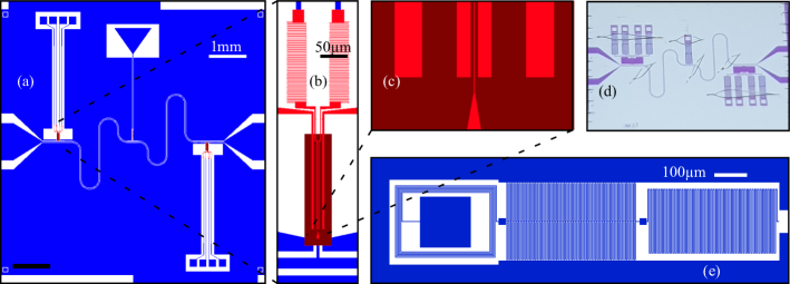
Figure 1 displays the geometry of the two analyzed devices. In each case the substrate is a wafer of 500 µm compensation doped silicon covered by 500 nm thermally grown SiO2 and a 100 nm niobium film. Fig. 1(a) shows the full lithograpy drawing of device A, in its geometry identical to the device used in Refs. 2, 3; Fig. 1(b) and Fig. 1(c) show details of it.
| measured at | device | ||
|---|---|---|---|
| after fabrication step | A | B | |
| 1 | resonator, dc conn., Nb filters, bond pads | 2500 | 2400 |
| 2 | gate finger electrode in the transfer area | 1800 | 1200 |
| 3 | cross-linked PMMA gate insulator | 1600 | |
| 4 | central Au filter, connection resonator-filter | 1600 | |
| 5 | contact electrodes in transfer area, Au filters | 420 | 1600 |
| 6 | deep etching of the adjacent trenches | 460 | 1700 |
As first fabrication step (step 1 in Table 1) the coplanar waveguide resonator, the dc bond pads, and their connecting lines are patterened in the niobium film using optical lithography (blue layer in Fig. 1(a-c)). Positive resist Microposit S1813 is spin-coated, exposed with a mask-aligner, and developed using developer AZ300-47. For the etch process, argon and sulphur hexafluorid is used in an Oxford Plasmalab reactive ion etching (RIE) system.
Next, electron beam lithography is used to define the 100 nm wide gate finger (red, in the center of Fig. 1(c); step 2 in Table 1). A polymethyl methacrylate (PMMA) bilayer (first layer molecular weight 200k 9% in anisole, second layer 950k 2% in anisole) is spin-coated, exposed, and developed with a mixture of methyl isobutyl ketone (MIBK) and isopropanole (IPA) in volume ratio 1:3. 10 nm titanium as adhesive layer are sputter-deposited, followed by thermal evaporation of 50 nm gold and lift-off in hot acetone.
In the following step, the gate insulator (brown in Fig. 1(a-c); step 3 in Table 1) is deposited as cross-linked PMMA: a PMMA bilayer is spin-coated and locally overexposed by a factor 20. This leads to cross-linking of the resist molecules and thus a 200 nm thick insulator layer insoluble in acetone and other process solvents, with a low relative dielectric constant of typically[9] .
Subsequently, the meander filter for the gate contact at the center of the resonator (red in Fig. 1(a), step 4 in Table 1) is defined, again via electron beam lithgraphy with a PMMA bilayer, metallization, and lift-off; here the gold thickness is 200 nm. The gold meander has a strip width of 500 nm and consist of 160 turns of each 18 µm length.
This is repeated for the four contact electrodes (source, drain, and two cutting elecrodes) in the transfer area and the meander filters connecting them (again, red in Fig. 1(a-c), step 5 in Table 1). The gold meanders for the four contacts have 120 turns of each 35 µm length.
As last step, deep trenches are etched on both sides of the contact electrodes to allow insertion of the quartz forks during nanotube transfer (geometry not shown in the figure; step 6 in Table 1).[8] We spin-coat two layers of AZ9260 photo resist and expose it using a mask aligner. AZ400K : water in ratio 1:2 is used as developer, follwed by RIE etching with argon and sulphur hexafluoride to a depth of 10 µm.
III Device geometry and fabrication steps, device B
Device B, depicted in Fig. 1(d-e), is an improved version where both the device geometry and (out of necessity) the fabrication steps have been adapted. The most distinct change is the introduction of niobium-based T-filters in each dc connection,[10] as shown in Fig. 1(e). These consist of a spiral inductor around a bond pad with 2 µm thick turns separated by a 2 µm wide gap, an interdigital capacitor that couples to the ground plane via 100 meshing fingers on both sides, 117 µm long and 2 µm wide separated by gaps of 2 µm, and finally a meander inductor 2 µm wide, separated by 2 µm gaps, with 100 turns of each 198 µm length. For the definition of the coplanar waveguide resonator a generic photomask without dc contacts is used; the filters are added subsequently via electron beam lithography and a second identical reactive ion etching process patterning the niobium layer (i.e., included in step 1 in Table 1).
To reduce the capacitive coupling between gate finger and contact electrodes, the contact electrodes (step 5) are additionally shortened; the “coupling length” , where gate and contacts run in parallel, is reduced from about 155 µm in device A to 86 µm in device B.
IV Transmission measurements at 4.2K
To identify detrimental processes, the devices were glued onto a sample carrier, bonded, and cooled down in a liquid helium vessel for microwave transmission measurement after each fabrication step. The temperature of the liquid helium, , is close enough to the critical temperature of niobium to still lead to a reduction of intrinsic resonator quality factors,[11, 7, 12, 13] however, any fabrication-induced reduction that is already visible here will also impact measurements at lower temperature. Thermalization of the device was done directly by immersion into the liquid helium, without any further low-temperature attenuation or isolation of the cables.
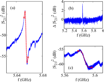
Figure 2 displays example transmission measurements. The curve of Fig. 2(a) shows the transmission of device B directly after definition of the coplanar waveguide resonator (step 1), at a vector network analyzer (VNA) output power . Fig. 2(b) shows a large frequency range plot of the difference in dB of two transmission measurements (i.e., the ratio of the measured transmissions) at and , now for device A after all fabrication steps (step 6). This allows an easy identification of the resonance among a noisy background, since at larger incident power the superconductivity within the coplanar waveguide resonator breaks down first. The corresponding raw data for device A, step 6 at is plotted in Fig. 2(c).
Fano resonances in transmission as visible in Fig. 2 are a well-known phenomenon and caused by parasitic channels bypassing the resonator. They can be modeled with the expression[14, 15]
| (1) |
where describes the overall transmission of the resonator, and its quality factor and resonance frequency, and and the transmission amplitude and phase of the parasitic channel. For extracting the quality factors, we fit to a selected interval of the measurement data. Due to the varying and irregular signal background, this selection clearly influences the result; this is the main source of error for the extracted and the reason why only rounded values are given in Table 1. In Fig. 2(a) and Fig. 2(c), the red line indicates the best fit function and the used interval.
The results are summarized in Table 1. Both devices start out at . Device A retains until after the deposition of the central bias connection to the resonator. With the fabrication of the source/drain electrodes, however, the quality factor sharply drops to , a value quite close to the one observed in Refs. 2, 3. The quality factor of device B, initially similar as for device A, decreases with the deposition of the gate finger, but then remains near until the end of the fabrication.
We can conclude that the optimizations have a clear effect; after all lithograhic steps, device B with its large, niobium-based filters and the shorter “coupling length” of the electrodes, where they run parallel to the gate finger, has a quality factor higher by approximately a factor 3.5 compared to device A. In addition, since in device A the definition of the source/drain electrodes was the critical step reducing , it is likely that the reduction of plays a role. From the experimental data it not possible yet to decide on the precise impact of the filter circuits.
V Comparison with numerical modeling
To gain further insight into the nature of resonator losses and the effectiveness of the different types of filters, the software package Sonnet Professional[16] has been used to model a simplified circuit geometry. Sonnet uses the so-called method of moments[17, 18] to calculate scattering matrix elements between circuit ports and is widely applied to problems in superconducting coplanar circuitry.
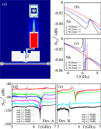
The substrate is modeled as stack of lossless insulators. The circuit geometry is segmented by the software in the initial calculation stages, with a minimum length scale set by user preference. To reduce calculation time we replace the fine gate finger electrode from the device geometries of Fig. 1 as well as the contact electrodes with two 5 µm wide niobium stripes running in parallel at a distance of 2 µm for a length of , see Fig. 3(a). In addition, for simplicity, the nanotube transfer region with contacts and filters is attached to a coplanar waveguide segment instead of a resonator.
Figure 3(a) shows the actual model geometry used in correspondence to device B. Ports 1 (signal input) and 2 (signal output) are terminated at the box walls of the calculated volume. A third port 3 connects the bond pad out of plane to ground; to approximate a dc wire connection, here we assume a termination with as well as an inductance of , the rule-of-thumb value for a 2 mm long wire bond.
In the variant of the geometry used for approximating device A, the niobium filter is replaced by a straight connection to the bond pad, and a fine gold meander identical to the one in the lithography drawing of device A is introduced directly at the edge of the transfer area.
Figures 3(b) and 3(c) display the calculation result for the Au-based filter and the Nb-based filter geometry, respectively. Both geometries lead to a clear filter resonance in the region . The current density plotted in Fig. 3(a) illustrates this at and . For the resistive gold meander, Fig. 3(b), a strongly broadened Fano function results, with an initially decreasing transmission at low frequency as well as an overall decrease of transmission. Measurement of the transmission of device A over a large frequency range, see Fig. 3(d), indeed confirm the presence of such a filter resonance with the same behaviour as soon as the gate finger electrode has been deposited and thus allows for a coupling between cavity and dc contact connections.
The filter resonance of the larger, niobium based filter is considerably sharper due to the superconductivity of the material (modelled as lossless metal), see Fig. 3(c). In addition, the Fano behaviour displays different polarity: the filter initially leads for frequencies below its resonance to suppressed damping, via constructive interference of the reflected signal. For larger , the resonance moves to lower frequencies. Fig. 3(e), a measurement of device B, clearly agrees with this result for the first two fabrication steps.
The filter resonance appears to be absent after deposition of the source/drain contacts (step 5). While from the data no definite explanation for this can be given, a striking detail is that here also the Fano shape of the microwave cavity resonance has changed its polarity. Via the much stronger coupling of the cavity to the dc connection and its filter, the filter resonance may have moved to significantly lower frequency. We can speculate that it may have merged with the cavity resonance or passed it entirely, with both signal contributions phase-shifted and again interfering constructively.
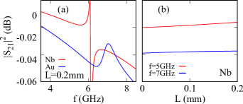
Additional modeling results are shown in Fig. 4. The power transmission as function of frequency for the two filter types is compared in Fig. 4(a) at . Again, this plot clearly demonstrates that the Au-based filters lead to damping, while at proper choice of parameters the Nb-based filter reflects the GHz signal back into the circuit for constructive interference. Figure 4(b) plots the transmission for the Nb-based geometry as function of the coupling length for and , i.e., below and above the filter resonances. As expected for the reflection mechanism, a stronger coupling of the dc connections here even counterintuitively improves the signal.
VI Conclusions and outlook
Two coplanar waveguide resonator devices including dc electrodes for microwave optomechanical experiments involving carbon nanotubes have been fabricated, with tests of low temperature GHz transmission properties after each step. Device A, identical in geometry with the device of Refs. 2, 3, includes a resistive gold meander in the dc connections, device B a niobium-based T-filter. We show experimentally that the quality factor of device A sharply drops with the fabrication of the source/drain electrodes, while device B retains a significantly higher up to the end of processing.
Model calculations using Sonnet Professional[16] on a simplified device geometry confirm these results. While the gold-based filter geometry leads to damping of the reflected signal, the niobium-based geometry can better reflect the signal back into the circuit, for constructive interference, minimizing losses and thereby in a full device maximizing . For the latter effect, a filter resonance plays an important role, a fact that will have to be taken into account for future device geometry planning.
While for superconducting two-level systems already multiple mechanisms to enhance optomechanical coupling have been proposed and implemented,[19, 20] for the particularly interesting case of carbon nanotube resonators this research is still at the start. Aside from quantum capacitance effects[2, 3, 21], also integrating carbon nanotubes as variable Josephson inductors is expected to lead to a strong coupling amplification.[22, 23] In addition to a modified GHz circuit geometry, this requires transparent contacts between superconductor and carbon nanotube,[24, 25, 26] in a device that keeps the carbon nanotubes suspended and thus nanomechanically active. Recent results[27] with gate voltage dependent critical currents in suspended, as-grown single-wall carbon nanotubes of up to 53 nA indicate that molybden-rhenium alloys[28, 11] provide a solution to this challenge, showing the way towards future optomechanical hybrid devices.
Acknowledgments
The authors acknowledge funding by the Deutsche Forschungsgemeinschaft via grants Hu 1808/4 (project id 438638106) and Hu 1808/5 (project id 438640202). This work was supported by the Academy of Finland project 312295 (CoE, Quantum Technology Finland). A. K. H. acknowledges support from the Visiting Professor program of the Aalto University School of Science. We would like to thank O. Vavra for experimental help, Ch. Strunk and D. Weiss for the use of experimental facilities, and A. N. Loh for insightful discussions. The measurement data has been recorded using Lab::Measurement [29].
References
References
- Aspelmeyer, Kippenberg, and Marquardt [2014] M. Aspelmeyer, T. J. Kippenberg, and F. Marquardt, “Cavity optomechanics,” Rev. Mod. Phys. 86, 1391–1452 (2014).
- Blien et al. [2020] S. Blien, P. Steger, N. Hüttner, R. Graaf, and A. K. Hüttel, “Quantum capacitance mediated carbon nanotube optomechanics,” Nature Communications 11, 1363 (2020).
- Hüttner et al. [2023] N. Hüttner, S. Blien, P. Steger, R. Graaf, and A. K. Hüttel, “Optomechanical coupling and damping of a carbon nanotube quantum dot,” (2023), arXiv:2304.02748 [cond-mat].
- Hüttel et al. [2009] A. K. Hüttel, G. A. Steele, B. Witkamp, M. Poot, L. P. Kouwenhoven, and H. S. J. van der Zant, “Carbon nanotubes as ultrahigh quality factor mechanical resonators,” Nano Letters 9, 2547–2552 (2009).
- Moser et al. [2014] J. Moser, A. Eichler, J. Güttinger, M. I. Dykman, and A. Bachtold, “Nanotube mechanical resonators with quality factors of up to 5 million,” Nature Nanotechnology 9, 1007–1011 (2014).
- Laird et al. [2015] E. A. Laird, F. Kuemmeth, G. A. Steele, K. Grove-Rasmussen, J. Nygård, K. Flensberg, and L. P. Kouwenhoven, “Quantum transport in carbon nanotubes,” Rev. Mod. Phys. 87, 703–764 (2015).
- Blien et al. [2016] S. Blien, K. J. G. Götz, P. L. Stiller, T. Mayer, T. Huber, O. Vavra, and A. K. Hüttel, “Towards carbon nanotube growth into superconducting microwave resonator geometries,” Phys. Stat. Sol. (b) 253, 2385 (2016).
- Blien et al. [2018] S. Blien, P. Steger, A. Albang, N. Paradiso, and A. K. Hüttel, “Quartz tuning-fork based carbon nanotube transfer into quantum device geometries,” Phys. Stat. Sol. B 255, 1800118 (2018).
- Brydson [1999] J. A. Brydson, Plastics Materials, 7th ed. (Butterworth-Heinemann, 1999).
- Hao, Rouxinol, and LaHaye [2014] Y. Hao, F. Rouxinol, and M. D. LaHaye, “Development of a broadband reflective T-filter for voltage biasing high-Q superconducting microwave cavities,” Applied Physics Letters 105, 222603 (2014).
- Götz et al. [2016] K. J. G. Götz, S. Blien, P. L. Stiller, O. Vavra, T. Mayer, T. Huber, T. N. G. Meier, M. Kronseder, C. Strunk, and A. K. Hüttel, “Co-sputtered MoRe thin films for carbon nanotube growth-compatible superconducting coplanar resonators,” Nanotechnology 27, 135202 (2016).
- Mattis and Bardeen [1958] D. C. Mattis and J. Bardeen, “Theory of the anomalous skin effect in normal and superconducting metals,” Phys. Rev. 111, 412–417 (1958).
- Gao et al. [2008] J. Gao, J. Zmuidzinas, A. Vayonakis, P. Day, B. Mazin, and H. Leduc, “Equivalence of the Effects on the Complex Conductivity of Superconductor due to Temperature Change and External Pair Breaking,” Journal of Low Temperature Physics 151, 557–563 (2008).
- Khalil et al. [2012] M. S. Khalil, M. J. A. Stoutimore, F. C. Wellstood, and K. D. Osborn, “An analysis method for asymmetric resonator transmission applied to superconducting devices,” Journal of Applied Physics 111, 054510 (2012).
- Petersan and Anlage [1998] P. J. Petersan and S. M. Anlage, “Measurement of resonant frequency and quality factor of microwave resonators: Comparison of methods,” Journal of Applied Physics 84, 3392–3402 (1998).
- Sonnet Software, Inc. [2022] Sonnet Software, Inc., “Sonnet Professional 18.56,” (2022), a detailed list of references for the used algorithms can be found on the product website, https://www.sonnetsoftware.com/.
- Harrington [1993] R. F. Harrington, Field computation by moment methods, IEEE Press series on electromagnetic waves (IEEE Press, Piscataway, NJ, 1993).
- Rautio and Harrington [1987] J. Rautio and R. Harrington, “An electromagnetic time-harmonic analysis of shielded microstrip circuits,” IEEE Transactions on Microwave Theory and Techniques 35, 726–730 (1987).
- Pirkkalainen et al. [2015] J.-M. Pirkkalainen, S. U. Cho, F. Massel, J. Tuorila, T. T. Heikkilä, P. J. Hakonen, and M. A. Sillanpää, “Cavity optomechanics mediated by a quantum two-level system,” Nature Communications 6, 6981 (2015).
- Schmidt et al. [2020] P. Schmidt, M. T. Amawi, S. Pogorzalek, F. Deppe, A. Marx, R. Gross, and H. Huebl, “Sideband-resolved resonator electromechanics based on a nonlinear Josephson inductance probed on the single-photon level,” Communications Physics 3, 1–7 (2020).
- Manninen et al. [2022] J. Manninen, M. T. Haque, D. Vitali, and P. Hakonen, “Enhancement of the optomechanical coupling and Kerr nonlinearity using the Josephson capacitance of a Cooper-pair box,” Physical Review B 105, 144508 (2022).
- Heikkilä et al. [2014] T. T. Heikkilä, F. Massel, J. Tuorila, R. Khan, and M. A. Sillanpää, “Enhancing optomechanical coupling via the Josephson effect,” Physical Review Letters 112, 203603 (2014).
- Rimberg et al. [2014] A. J. Rimberg, M. P. Blencowe, A. D. Armour, and P. D. Nation, “A cavity-Cooper pair transistor scheme for investigating quantum optomechanics in the ultra-strong coupling regime,” New Journal of Physics 16, 055008 (2014).
- Buitelaar et al. [2003] M. R. Buitelaar, W. Belzig, T. Nussbaumer, B. Babić, C. Bruder, and C. Schönenberger, “Multiple Andreev reflections in a carbon nanotube quantum dot,” Physical Review Letters 91, 057005 (2003).
- Jarillo-Herrero, van Dam, and Kouwenhoven [2006] P. Jarillo-Herrero, J. A. van Dam, and L. P. Kouwenhoven, “Quantum supercurrent transistors in carbon nanotubes,” Nature 439, 953–956 (2006).
- Jørgensen et al. [2006] H. I. Jørgensen, K. Grove-Rasmussen, T. Novotný, K. Flensberg, and P. E. Lindelof, “Electron transport in single-wall carbon nanotube weak links in the Fabry-Perot regime,” Physical Review Letters 96, 207003 (2006).
- Kaikkonen et al. [2020] J.-P. Kaikkonen, A. T. Sebastian, P. Laiho, N. Wei, M. Will, Y. Liao, E. I. Kauppinen, and P. J. Hakonen, “Suspended superconducting weak links from aerosol-synthesized single-walled carbon nanotubes,” Nano Research 13, 3433–3438 (2020).
- Schneider et al. [2012] B. H. Schneider, S. Etaki, H. S. J. van der Zant, and G. A. Steele, “Coupling carbon nanotube mechanics to a superconducting circuit,” Scientific Reports 2, 599 (2012).
- Reinhardt et al. [2019] S. Reinhardt, C. Butschkow, S. Geissler, A. Dirnaichner, F. Olbrich, C. Lane, D. Schröer, and A. K. Hüttel, “Lab::Measurement — a portable and extensible framework for controlling lab equipment and conducting measurements,” Computer Physics Communications 234, 216–222 (2019).