Ferroelastic twin angles at the surface of CaTiO3 quantified by PhotoEmission Electron Microscopy
Abstract
We use photoemission electron microscopy to measure the ferroelastic twin wall angles at the surface of CaTiO3(001) and deduce the strain ordering. We analyze the angular dependence of the photoelectron emission from different domain surfaces, each with their own characteristic tilt angle in the factory roof-like topography. By considering the surface topography as a field perturbation, the offset in the photoemission threshold can be directly related to the tilt angles. With knowledge of the symmetry allowed twin walls we quantify twin topography between 179.1° to 180.8°.
At twin boundaries in ferroelastic materials, the spontaneous strain changes sign over only a few nanometers [1] giving rise to strong gradients which can generate new properties quite distinct from those of the adjacent domains. Superconductivity [2], polarity [3, 4] and chirality [4] have all been reported in twin walls. Such emerging functionalities are absent in the bulk [5, 6] and provide a new perspective of “the material is the machine” [7]. In addition, their nanometric dimensions make them potentially 2D functional objects.
The polar character of twin walls was predicted theoretically [8] and simulations suggest that twin wall polarity in CaTiO3 and SrTiO3 [9] can be switched by an applied field [10]. If this were the case then ferroelastic materials with ferroelectric twin walls would be promising for robust, high-density information storage. Harnessing such functionality requires controlling twin wall polarity at the surface which, in turn, depends on the strain state of the domain twins.
Twinning gives rise to surface topography with a characteristic factory roof-like structure. Each twin has a distinct angle at the surface, often within a degree of 180° (flat surface) defined by the strain tensor compatibility across the wall [11]. The tensors in turn define the local strain gradients and therefore directly influence both the magnitude of the wall polarity and, potentially, the switching field. Novak and Salje studied the distribution of lattice strain near the intersection of surface layers and twin boundaries [12]. They found that twin boundaries close to the surface show a groove-ridge profile on each side of the twin boundary which are expected to generate local polarization via the flexoelectric [13] (or other) coupling effects [14]. Quantification of the twin angles at the surface of ferroelastic materials is therefore an essential step towards demonstrating polarity switching in ferroelastic twin boundaries and understanding the electromechanical coupling between strain and polarity.
CaTiO3 is the archetypal perovskite, ferroelastic below 1150°C with a Pbnm orthorhombic structure. It consists of corner-linked TiO6 octahedra with Ca atoms sitting in between, distorted from the ideal cubic perovskite by two independent octahedral tilts written as a-a-c+ in Glazer notation [15]. By symmetry, one of the tilts goes to zero at the twin wall, allowing for the emergence of a competing secondary order parameter [4]. Biquadratic coupling between the primary and secondary order parameter yields two equivalent ground states for the wall polarity [14]. However, the flexoelectric induced strong polarization [16] may break inversion symmetry and favor a specific polarization direction in the twin wall.
Twin walls in CaTiO3 have been studied using aberration-corrected transmission electron microscopy [3]. Second harmonic generation (SHG) provides another proof of the loss of inversion symmetry [11] but with a spatial resolution limited to 0.5 m. Eliseev et al. have carried out a theoretical study of the DW/surface intersection in CaTiO3 [17]. However, little work exists on the direct measurement of the twin angles. Electron imaging of charged (ferroelectric) surfaces was proposed by Le Bihan [18] and successfully applied to visualize ferroelastic domains in barium titanate while low energy electron microscopy has yielded valuable data on CaTiO3 surface topography and structure [19, 20].
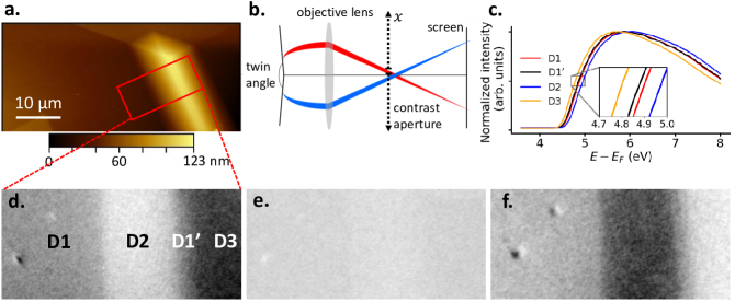
Energy-filtered PhotoEmission Electron Microscopy (PEEM) is a non-destructive, surface-sensitive imaging technique with a high spatial and energy resolution. Contrast in PEEM arises from local chemistry, work function [21], electrical or physical topography [22, 23]. We have developed a quantitative approach using the specificities of photoemission electron microscopy to determine the twin angle present at the surface of CaTiO3 thanks to a simple model of the imaging electron optics. This has been done by exploring the angular space of the PEEM images, specifically, electrons cross the diffraction plane on the optical axis for normal emission and off-axis for off-normal emission. By positioning an aperture in the back focal plane, a given angular range can be selected to quantify the twin angles.
Optical microscopy and atomic force microscopy (AFM) are also sensitive to the surface topography, however, the lateral resolution of PEEM (50 nm) is much better than optical microscopy while AFM is a scanning technique. The high resolution of parallel imaging of PEEM also opens the perspective of studying ferroelastic domain dynamics.
The sample is a CaTiO3 (001) single crystal from SurfaceNet GmbH. Before introduction into the vacuum system, the sample was exposed for 5 min to ozone at room temperature to remove the organic contamination. Annealing at 650°C in vacuum is used to desorb the oxidized contaminants and produces near surface oxygen vacancies, helping to alleviate charging problems during the photoemission process [19]. Experiments were carried out at 300°C to further avoid charging. A focused He I source (21.2 eV) was used in a ScientaOmicron NanoESCA II PEEM. Photoemission threshold image series are acquired as a function of the electron energy with respect to the sample holder Fermi level, , in steps of 50 meV and with an energy resolution of 100 meV, as determined by the analyzer slit and pass energy. Images are normalized with respect to the signal from a homogeneous area of the sample in order to account for detector inhomogeneities. The image series were analyzed using an automatic procedure fitting the pixel-by-pixel threshold spectra with an error function [24]. The non-isochromaticity in the vertical direction due to the dispersion in the hemispherical imaging analyzer is corrected [24]. The contrast aperture (CA) in the back focal plane has a diameter of 150 m. Image series were acquired for CA positions between -230 m and + 230 m in steps of 10 m with respect to the optical axis.
Complementary AFM was performed using a Nano-Observer (CS-Instruments) in contact mode with FORTA tips (AppNano) with stiffness of 1.6 N/m to characterize the surface without scratching.
The effect of the CA is shown in the schematic of Fig. (1b). Higher off-centering of the CA improves dramatically the domain topography contrast in PEEM thanks to the angular selection but also induces a shift of the energy scale. Off-normal electrons have velocity components perpendicular and parallel to the sample surface, as a result, the kinetic energy measured inside the PEEM will be slightly lower, and the threshold for photoemission is shifted to higher energy within the reference frame of the PEEM.
Emission from domains with different tilt angles are centered at different positions in the diffraction plane, giving rise to intensity variation as shown in Fig. 1d-f via the angular selection by the CA (Fig.1b). We focus on the domains labeled D1, D2, D and D3. Domain D1 is used for PEEM electron optics alignment and the surface normal coincides with the PEEM optical axis. D2, D3 and D have finite tilt angles with respect to D1. The twin wall is vertical, therefore, by off-centering the CA horizontally we selectively analyze photoelectrons emitted from domains (Fig.1d and f) on either side of a twin boundary. When the CA is centered on the optical axis, the contrast between the twin domains is almost zero. In this configuration, the angular difference with respect to D1 is minimized as in Fig.1e. Figure 1(c) shows the spectra for each domain extracted from the threshold image series.
The threshold values are obtained by performing a pixel-by-pixel fit to the spectra with an error function, giving a map of threshold values, as detailed in Supp mat. Figure 2 shows the evolution of the photoemission threshold for D1, D2, D, and D3 of Fig.1 as a function of the CA position from –230 m to +230 m.
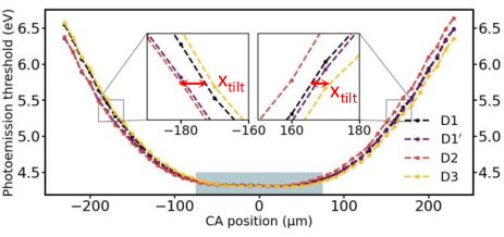
Close to the optical axis, the measured threshold is constant at 4.05 eV. When the CA is off-centered further than its physical radius (75 m), electrons on the optical axis are physically blocked, effectively switching to a dark field imaging mode where higher angle emission from one side of the optical axis is enhanced at the expense of emission from the other side. The contrast between domains is enhanced (Fig.1d,f) not only because the threshold value increase but also because the difference between domain thresholds increases. The threshold energy curves have the same form but they are not centered at the same CA position. D2 and D3 have surface tilts of opposite signs and are rigidly shifted respectively to the left and right with respect to that of D1 and D. When the domain surface is tilted by an angle the photoelectron intensity in the back focal plane is also off-centered by a distance , experimentally obtained from the centroid of the two parabolic branches in Fig. 2. Therefore, by measuring the shift in the threshold curves and with a knowledge of the electron optics, it should be possible to quantify the twin angles, as suggested in Fig. 3.
Phase conservation in the PEEM is given by
| (1) |
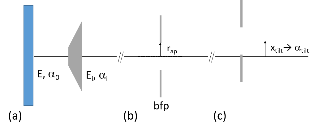
where the emission angle with respect to the sample normal, the electron energy in the PEEM column, the electron angle with respect to the optical axis in the PEEM. The objective lens magnification M is defined as /. For small angles, where l is the distance between the CA and the first image plane. For simplicity, we assume an isotropic electron emission up to 90°, i.e. . For a tilted surface, the optical axis in the back focal plane is shifted by xtilt. The photoemission threshold is given by equation 2 (details in supplementary materials).
| (2) |
The evolution of the photoemission threshold with the CA lateral position is therefore a stretched parabola with a flat central range defined by of constant minimum threshold. In the NanoESCA setup, = 165 mm, = 32 and = 2000 eV, which allows to extract at each pixel. From , we can then work back to the surface tilt angle by considering a periodic triangular surface topography as a perturbation of the local electric field [25] (details in supplementary materials). Equation 3 expresses the relation between the surface tilt angle and the CA position in the back focal plane .
| (3) |
with ck is the conversion factor between position in the back focal plane and reciprocal lattice vector for the PEEM settings used here (4.14 ), the electron mass, the bias between the sample and extractor (20 kV), the surface topography periodicity and the distance between the sample and extractor. The angle map is represented in Fig.4a and compared with that measured by AFM.
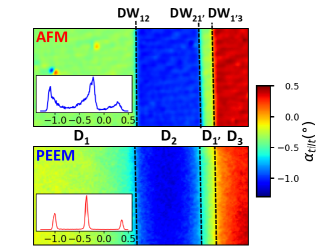
There is a good qualitative agreement between the PEEM and AFM maps. The PEEM analysis correctly discriminates the ferroelastic domains D1, D2, D and D3. Surfaces tilted with a positive or negative angle are revealed and the narrow domain D between D2 and D3, which has the same angle as D1 is also resolved. The latter has a domain width of 1.7 m. It should be noted that the usual method in the PEEM of imaging in the reciprocal space to deduce surface angles would have been impossible for a domain this small since it is beyond the limit of usual field apertures. High resolution real-space imaging to deduce angular maps with the sub-micron resolution is necessary.
The histograms of the PEEM and AFM angular maps are shown in the insets of Fig. 4. The overall angular range, as determined by PEEM is between -1.25° and 0.45°, in agreement with the known CaTiO3 twin angles [19]. D2 and D3, centered at -1.0° and +0.4°, respectively, show good agreement between AFM and PEEM. The main discrepancy between the two angular maps remains the tilt angle of D1. This is due to the residual alignment offset between PEEM and AFM.
The angular spread for D1 and D2 is much smaller in AFM compared to the PEEM, typically 0.05° compared to 0.15°. The higher angular spread for the PEEM data is related to the finite aperture size of the electron optics. The finite CA radius allows a spread in acceptance angles and hence in threshold values, contrary to the AFM analysis. A second factor is that the PEEM acquires data by parallel imaging at fixed lens parameters. There is a weak correlation even for microscopic fields of view between position and take-off angle which adds to the angular broadening whereas AFM acquires data sequentially, at each data point measuring the same slope, and is immune to angular cross-talk.
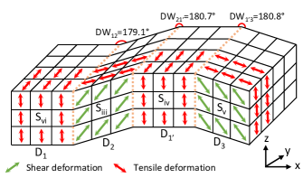
The twin angles calculated from the values are DW12 = 179.1° 0.2°, DW = 180.7 0.2°, and DW = 180.8 0.2° and are reported in table 1.
| DW12 | DW | DW | |
|---|---|---|---|
| Twin angle | 179.1° 0.2° | 180.7 0.2° | 180.8 0.2° |
| Strain state | Svi/Siii | Siii/Siv | Siv/Sv |
There are six possible spontaneous strain orientations in CaTiO3 which satisfy stain compatibility deduced from symmetry [26, 11, 19]. Given the experimental angles, the twin walls are of type W [11] and are described by x = y. From the sequence 179.1°/180.9°/180.9°, we deduce a strain ordering of Svi/Siii/Siv/Sv (supp mat), as represented in Fig. 5 and summarized in table 1.
This analysis is limited to domains aligned vertically in the PEEM, i.e. running orthogonal to the lateral displacement of the CA. However, it would be straightforward to extend the methodology to two dimensions to analyze twin structures along all combinations of and by using the full x-y in-plane positions of the CA. As discussed, the finite CA radius gives rise to an angular spread, however, in the limit of small angles, this does not influence the mean twin angles.
We have used threshold PEEM imaging to measure twin angles at the surface of ferroelastic CaTiO3 with its characteristic factory roof-like structure. By off-centering the contrast aperture from the optical axis, contrast due to the physical surface topography is enhanced by collecting high angular photoelectrons in a near dark-field mode. Electrons emitted at higher angles have a higher apparent value of the photoemission threshold. Using a model of the electron optics, integrating the perturbation of the extractor field by surface twin topography we can quantify the twin angles, and by comparison with the symmetry allowed twin walls we can deduce directly the surface strain ordering. The results agree well with the independent measurements by AFM. They provide a unique insight into electromechanical coupling responsible for twin wall polarity at the surface and, potentially, a handle to control twin wall polarity.
References
- Hayward et al. [1997] S. A. Hayward, J. Chrosch, E. K. H. Salje, and M. A. Carpenter, European Journal of Mineralogy 8, 1301 (1997).
- Aird and Salje [1998] A. Aird and E. K. H. Salje, Journal of Physics: Condensed Matter 10, L377 (1998).
- Van Aert et al. [2012] S. Van Aert, S. Turner, R. Delville, D. Schryvers, G. Van Tendeloo, and E. K. H. Salje, Advanced Materials 24, 523 (2012).
- Goncalves-Ferreira et al. [2008] L. Goncalves-Ferreira, S. A. Redfern, E. Artacho, and E. K. Salje, Physical Review Letters 101, 1 (2008).
- Salje and Zhang [2009] E. Salje and H. Zhang, Phase Transitions 82, 452 (2009).
- Viehland and Salje [2014] D. D. Viehland and E. K. Salje, Advances in Physics 63, 267 (2014).
- Bhattacharya and James [2005] K. Bhattacharya and R. D. James, Science 307, 53 (2005).
- Janovec and Přívratská [2006] V. Janovec and J. Přívratská, in International Tables for Crystallography (International Union of Crystallography, Chester, England, 2006) pp. 449–505.
- Scott et al. [2012] J. F. Scott, E. K. Salje, and M. A. Carpenter, Physical Review Letters 109, 1 (2012).
- Zykova-Timan and Salje [2014] T. Zykova-Timan and E. K. Salje, Applied Physics Letters 104 (2014), 10.1063/1.4866859.
- Yokota et al. [2014] H. Yokota, H. Usami, R. Haumont, P. Hicher, J. Kaneshiro, E. K. Salje, and Y. Uesu, Physical Review B - Condensed Matter and Materials Physics 89, 1 (2014).
- Novak and Salje [1998] J. Novak and E. K. H. Salje, Journal of Physics: Condensed Matter 10, L359 (1998).
- Zubko et al. [2013] P. Zubko, G. Catalan, and A. K. Tagantsev, Annual Review of Materials Research 43, 387 (2013).
- Salje et al. [2016] E. K. H. Salje, S. Li, M. Stengel, P. Gumbsch, and X. Ding, Physical Review B 94, 024114 (2016).
- Glazer [1972] A. M. Glazer, Acta Crystallographica Section B Structural Crystallography and Crystal Chemistry 28, 3384 (1972).
- Stengel [2013] M. Stengel, Physical Review B 88, 174106 (2013).
- Eliseev et al. [2012] E. A. Eliseev, A. N. Morozovska, Y. Gu, A. Y. Borisevich, L. Q. Chen, V. Gopalan, and S. V. Kalinin, Physical Review B - Condensed Matter and Materials Physics 86, 1 (2012).
- Le Bihan [1989] R. Le Bihan, Ferroelectrics 97, 19 (1989).
- Nataf et al. [2017] G. F. Nataf, M. Guennou, J. Kreisel, P. Hicher, R. Haumont, O. Aktas, E. K. H. Salje, L. Tortech, C. Mathieu, D. Martinotti, and N. Barrett, Physical Review Materials 1, 074410 (2017).
- Zhao et al. [2019] Z. Zhao, N. Barrett, Q. Wu, D. Martinotti, L. Tortech, R. Haumont, M. Pellen, and E. K. Salje, Physical Review Materials 3, 1 (2019).
- Escher et al. [2010] M. Escher, K. Winkler, O. Renault, and N. Barrett, Journal of Electron Spectroscopy and Related Phenomena 178-179, 303 (2010).
- Nepijko et al. [2001] S. A. Nepijko, N. N. Sedov, and G. Schonhense, Journal of Microscopy, Tech. Rep. (2001).
- Lavayssière et al. [2013] M. Lavayssière, M. Escher, O. Renault, D. Mariolle, and N. Barrett, Journal of Electron Spectroscopy and Related Phenomena 186, 30 (2013).
- Barrett et al. [2013] N. Barrett, J. E. Rault, J. L. Wang, C. Mathieu, A. Locatelli, T. O. Mentes, M. A. Niño, S. Fusil, M. Bibes, A. Barthélémy, D. Sando, W. Ren, S. Prosandeev, L. Bellaiche, B. Vilquin, A. Petraru, I. P. Krug, and C. M. Schneider, Journal of Applied Physics 113 (2013), 10.1063/1.4801968.
- Bok [1968] A. Bok, A mirror electron microscope, PhD Thesis, http://resolver.tudelft.nl/uuid:a0046b97-8e35-4878-bb4c-ebc065727e20 (1968).
- Sapriel [1975] J. Sapriel, Physical Review B 12, 5128 (1975).