Performance of TES X-Ray Microcalorimeters Designed for 14.4-keV Solar Axion Search
Abstract
A 57Fe nucleus in the solar core could emit a 14.4-keV monochromatic axion through the M1 transition if a hypothetical elementary particle, axion, exists to solve the strong CP problem. Transition edge sensor (TES) X-ray microcalorimeters can detect such axions very efficiently if they are again converted into photons by a 57Fe absorber. We have designed and produced a dedicated TES array with 57Fe absorbers for the solar axion search. The iron absorber is set next to the TES, keeping a certain distance to reduce the iron-magnetization effect on the spectroscopic performance. A gold thermal transfer strap connects them. A sample pixel irradiated from a 55Fe source detected 698 pulses. In contrast to thermal simulations, we consider that the pulses include either events produced in an iron absorber or gold strap at a fraction dependent on the absorption rate of each material. Furthermore, photons deposited on the iron absorber are detected through the strap as intended. The identification of all events still needs to be completed. However, we successfully operated the TES with the unique design under iron magnetization for the first time.
Keywords:
(Sensors, Microcalorimeters, TES, Solar axions, Monochromatic axion, 57Fe)1 Introduction of Solar Axion Search and TES Detection Sensitivity
An axion is a hypothetical elementary particle proposed to solve the strong CP problem in quantum chromodynamics [1, 2]. The axion is one of the dark matter candidates required in the current cosmology. The axion can convert to a photon or vice versa in a certain probability via the axion-photon coupling in an external electric or magnetic field. At the center of the Sun, photons of [3] could produce axions by the interaction with the magnetic field, and their energy spectrum traces the blackbody radiation [4]. In addition to this process, magnetic dipole (M1) transitions of some nuclei, which can be excited thermally, could also produce axions via the axion-nucleon coupling. 57Fe nuclei have an M1 transition level of , and Moriyama 1995 [5] calculated the monochromatic axion flux from the Sun at . These monochromatic axions would excite the same 57Fe nuclei in a laboratory on the Earth and would be reconverted to 14.4-keV photons. Moriyama (1995) [5] also proposed to search for solar axions by detecting these photons. Moreover, this method has the advantage that the detector does not need to be tuned to the axion mass, unlike dark-matter axion searches.
A silicon-based semiconductor detector searched the 14.4-keV photons from 57Fe film [6, 7, 8, 9, 10], and the best upper limit on axion mass of [10] is obtained at 95% confidence limit in the KSVZ hadronic axion model [11]. Other experiments using a proportional gas chamber to detect 9.4-keV photons from 83Kr gas bounded on the hadronic axion mass of (95% C.L.) [12, 13]. In the 57Fe film experiment, the branching ratio to emit a 14.4-keV photon is only 10.5%, and the rest are converted to electrons or low-energy X-rays. Moreover, the iron film itself absorbs about 80% of the photons. The combination of an iron film and any silicon-based detectors was not able to detect the self-absorbed thermal energy from axions in the film. Therefore, the detection efficiency was not more than 10%. We came up with the idea that a transition edge sensor (TES) X-ray microcalorimeter array with 57Fe absorbers could be a solar axion detector. This is because the microcalorimeters can detect not only 14.4-keV photons but also all dissipated energy in the absorbers. Also, the excellent energy resolution of TES microcalorimeters would improve the sensitivity for the monochromatic axions, with enough converter mass and exposure time.
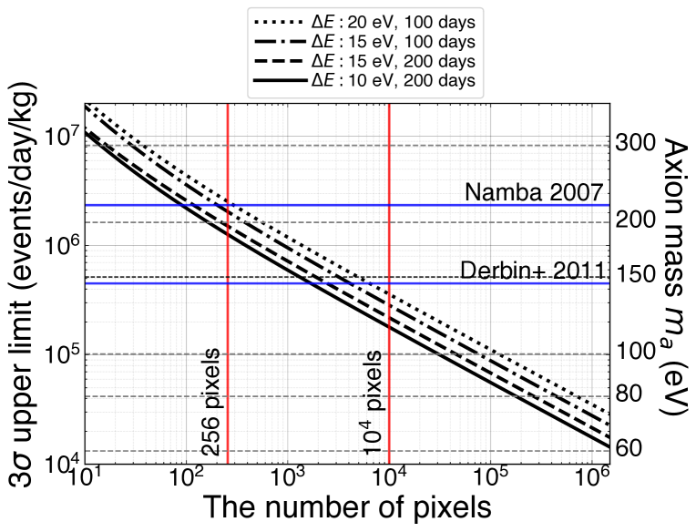
We assume a 57Fe axion converter size of and an iron density of . The on-ground background rate of the X-ray spectrometer (XRS) for Suzaku observatory using the anti-coincidence detector was [14]. We conservatively expect the background rate of . Our group achieved the full width at half maximum (FWHM) energy resolution of at [15] and successfully fabricated a 64-pixel TES array [16]. Figure 1 shows the estimated detection limits against the number of pixels (i.e., axion converter mass), with various energy resolutions and exposure times. A detection limit can be converted into an axion mass limit with Eq. 3 and 7 in [5]. Here, parameter values of , , , and in the hadronic axion [17] are used. As a simultaneous readout of 38 TES pixels via microwave multiplex (MWMUX) readout system [18] has been demonstrated [19, 20], the production of a extensive format array system is promising with our technologies.
2 Microcalorimeter Design and Fabrication
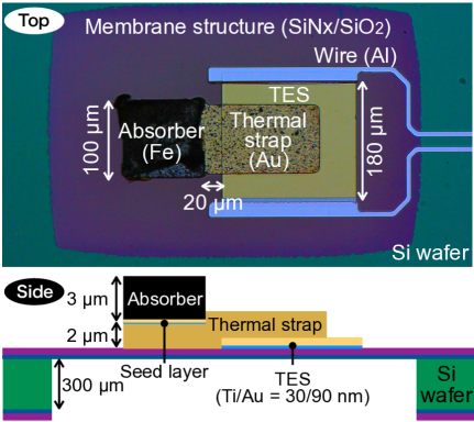
The energy resolution of TES could degrade if it is operated under a magnetic field made by a ferromagnetic iron absorber. The effect depends on the direction of the field through a TES [21]. The perpendicular magnetic field affects badly, but the horizontal field does not. In order to reduce the magnetic field on the TES, we located the iron absorber next to the TES and connected them with a gold thermal transfer strap, as shown in Fig. 2. We have estimated that the magnetic field becomes less than , where we were able to operate TES microcalorimeters without trouble if the distance from the edge of a 5--thickness iron is more than [22]. Konno et al. 2020 [22] showed the possible degradation of energy resolution, from to , by the position dependence in the iron absorber under the condition where the conductivity of iron and that of gold are and at , respectively. Large enough thermal conductivities of both iron and gold are required.
To form thick iron absorbers, we have been developing a recipe for electroplating pure iron in the facilities of the Nanotechnology Research Center (NTRC) at Waseda University. Electroplating is very effective method to produce a small structure with expensive materials like a 57Fe isotope. Although we need a high density and good thermal conductivity in the absorber, pure iron is rarely used commercially, and thus standard process has not yet been established. We made several test samples by reacting in an iron-liquid solution of not expensive normal 56Fe. We measured electric resistances at room temperature and using the LR-700 AC resistance bridge of Linear Research Inc. We achieved effective deposition even in low solution concentration, 0.05 mol/L, after adjusting the electric current, the time, and additions in the solution. The thermal conductivities, – at , calculated from the Wiedemann-Franz law, were more than 30 times higher and more efficient heat transmission than the former worst case value, , used in the estimation of the degradation by position dependence [22].
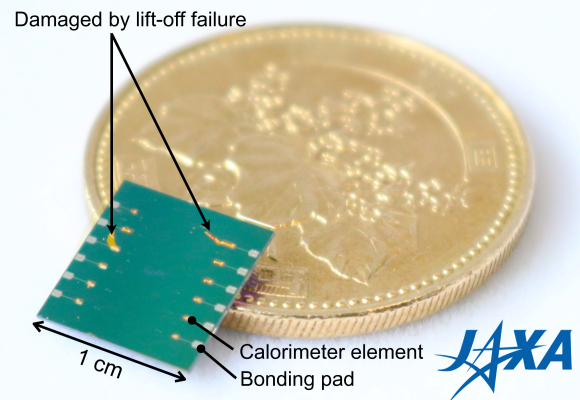
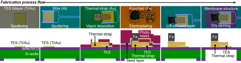
We fabricated a test device of this newly designed TES microcalorimeter in the nanoelectronics clean room at ISAS/JAXA in a process flow shown in Fig. 3. Firstly, proximity-coupled titanium/gold TES bilayer was deposited by sputtering, and aluminum leads were attached. Secondly, gold thermal transfer straps of 2- thickness were evaporated by the electron beam physical vapor deposition. Thirdly, iron absorbers of 3- thickness were electroplated on the electrode seed layer. Then, the film was electroplated twice because the target thickness was not reached the first time. The device has various distances, 0, 20, 60, 100, 200, 300, and 500 , between an iron-absorber edge and a TES edge to avoid the magnetic field from the iron absorber. Finally, membrane structures of SiNx/SiO2 under TES were formed by a deep reactive ion etching. Sixteen pixels out of twenty-four were successfully produced, as shown in Fig. 2. We have not yet established the fabrication process completely. Some photoresist compositions remained and made wrinkles after iron electrodeposition in Fig. 3. The lift-off of the seed layers failed in some pixels in Fig. 2, left. We suspect that the rough gold surface, due to the high deposition rate, caused an adhesion reduction with the seed layer on the straps.
3 Non-uniformity of Iron Absorber and Investigation by Material Analysis
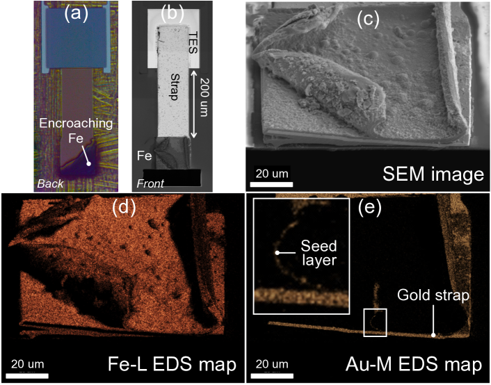
We observed the fabricated chips and found unexpected black materials from the back in all elements after membrane structure formation, as shown in Fig. 4, a. As the iron surface was rough and curled, we suspected that the irons, designed only on gold thermal straps, were deposited wrongly. For analyzing these materials, an element was vertically cut with a focused ion beam (FIB) (Fig. 4, b), and we observed the cross-section by the scanning electron microscope (SEM) and energy dispersive X-ray spectroscopy (EDS) (Fig. 4, c, d, e). These images indicate that the iron and the seed layer curled up together due to the iron tensile stress in an early phase of the first electroplating, and then the gold strap was also peeled off partially from the wafer. In the second electroplating, the iron structures were deposited under the seed layer and on and under the gold strap. Although the size of the gold strap has a 5- extra margin to the iron size not to protrude from the strap, if the photolithographic pattern on the strap is out of alignment by more than the margin, a gap between a photoresist and a strap edge occurs. Therefore, the iron solution could encroach on the back of the gold straps from the gap. This hypothesis indicates that more accurate pattering or designing the larger strap area than the iron absorber is favored. Also, to increase the adhesion between the seed layer and the strap, a new gold electroplating process for straps is under testing to fabricate smoother surfaces. In general, the electroplating makes 10 times higher thermal conductivity at compared to the vapor deposition we used this time. The residual resistance ratio (RRR) of to is around 30 [23].
4 X-Ray Irradiation Test and Pulse Shapes
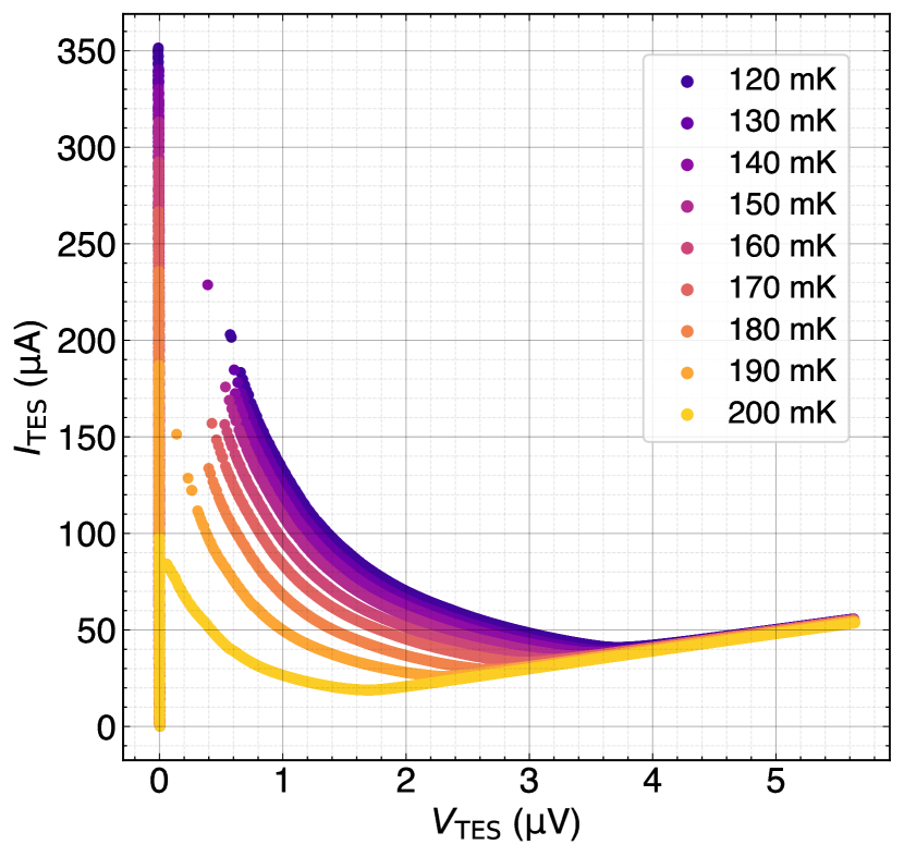
We performed an X-ray irradiation test under a cryogenic temperature of an iron-absorber-TES microcalorimeter with a - distance between the absorber and the TES (Fig. 2). Figure 5 shows the measured IV curve at different bath temperatures. An X-ray source (55Fe isotope) and a silicon collimator were mounted above the chip at about and , respectively. The normal state resistance is . The transition temperature was , and the operating temperature was set to . The ( is around 100. The TES was connected to a superconducting quantum interference device (SQUID) amplifier and operated under a standard electro-thermal feedback (ETF) method.
In about three days, 698 waveforms of signal pulses were recorded with a time resolution of . The pulse shapes were not identical or similar. These were divided into two types. ”Normal” type pulses are characterized by their rising time in the order between microseconds and milliseconds and by the falling time in a few milliseconds. Others are called ”Spike” type pulses because a few microseconds fast spike is seen at the beginning of the pulses, followed by a slow falling time in about a millisecond. The pulse events were classified into nine groups by their pulse shapes, and averaged pulses in each group are shown in Fig. 6. The number of pulses, rising time , and falling time in each group are in Tab. 1. X-ray radiation spread over the vicinity of the iron absorber, including the thermal strap and TES area, because the collimator was not small enough compared to the distance from the chip. Consequently, X-rays could deposit at the absorber, thermal strap, TES, and membrane and make signal pulses with different time scales. We are working on reproducing obtained pulse shapes with a realistic thermal model using a finite element method with COMSOL Multiphysics software [24] to identify the event location by pulse shapes. According to the simulation, the iron absorber and the thermal strap events have similar pulse shapes. Regardless of absorbing positions in the absorber or strap, events up to about far from the TES edge have a spike shape, and events farther than that have a normal shape. The falling times of both shapes are . In either of the pulse shapes, the rise time of absorber events is about – and is faster and closer to the TES. On the other hand, the thermal strap events under Fe are about the same, and the events closer to TES have an even faster rising time. They are comparable with Group N1 and S in Tab. 1. Therefore, the obtained data include both the iron absorber and gold strap events at a fraction dependent on the absorption rate of each material. As intended, the X-ray photons deposited on the iron absorber are detected through the thermal strap.
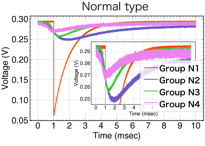
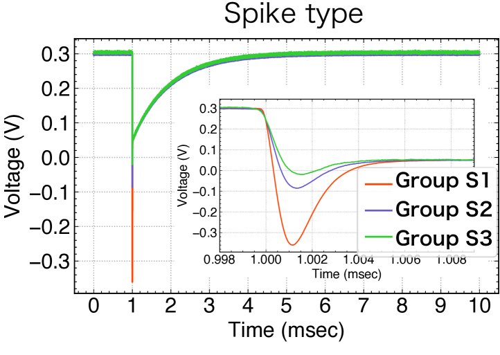
| Pulse type | Normal type | Spike type | |||||||
|---|---|---|---|---|---|---|---|---|---|
| Group | N1 | N2 | N3 | N4 | The others | S1 | S2 | S3 | The others |
| Number | 151 | 57 | 117 | 20 | 33 | 206 | 80 | 18 | 16 |
| () | 0.40–1.7 | 4.0 | (1.0–3.0) | (1.3–2.5) | - | 0.70–0.90 | 1.0–1.2 | 1.2–1.4 | - |
| (ms) | 0.80–0.90 | 4.0–5.3 | 1.2–2.2 | 0.10–0.30 | - | 0.80–1.0 | 0.90–1.0 | 0.90–1.0 | - |
5 Conclusion and Future Prospects
We successfully deposited iron absorbers whose thermal conductivities are – at using 56Fe and produced the first test calorimeters for the solar axion detector. In irradiation tests, it was likely that iron events were detected. The identification of all events still needs to be completed. However, for the first time, we successfully operated the TES microcalorimeter with a certain distance between the iron absorber and the TES under iron magnetization. The high thermal conductivity of gold thermal straps could decrease the effect of degrading the energy resolution by the position dependence in an absorber discussed in [22]. To make efficient detectors, we try to deposit gold straps by electroplating and continue to fabricate iron absorbers with high conductivity.
Acknowledgements.
We are grateful to S. Moriyama for his suggestions about solar axion searches. Our research was partially performed in the nano-electronics clean room at the Institute of Space and Astronautical Institute (ISAS). We also thank the technical staff members of the Nanotechnology Research Center (NTRC) at Waseda University and the National Institute for Materials Science (NIMS). The SQUID array amplifier used for irradiation tests was fabricated by the clean room for analog & digital superconductivity (CRAVITY) of the National Institute of Advanced Industrial Science and Technology (AIST). The Japan Society financially supported this work for the Promotion of Science (JSPS) KAKENHI Grant Number 18H01244 and 20H05857.References
-
1
R. D. Peccei and H. R. Quinn, Phys. Rev. Lett. 38, 1440, (1977), DOI: 10.1103/PhysRevLett.38.1440;
R. D. Peccei and H. R. Quinn, Phys. Rev. D 16, 1791, (1977), DOI: 10.1103/PhysRevD.16.1791. -
2
S. Weinberg, Phys. Rev. Lett. 40, 223, (1978), DOI: 10.1103/PhysRevLett.40.223;
F. Wilczek, Phys. Rev. Lett. 40, 279, (1978), DOI: 10.1103/PhysRevLett.40.279. - 3 S. Turck-Chize, W. Dppen, E. Fossat, J. Provost, E. Schatzman, and D. Vignaud, Phys. Rep. 230, 57, (1993), DOI: 10.1016/0370-1573(93)90020-E.
-
4
K. van Bibber, P. M. McIntyre, D. E. Morris, and G. G. Raffelt, Phys. Rev. D 39, 2089, (1989), DOI: 10.1103/PhysRevD.39.2089;
F. Hoogenveen and R. G. Stuart, Phys. Lett. B 286, 165, (1992), DOI: 10.1016/0370-2693(92)90175-4. - 5 S. Moriyama, Phys. Rev. Lett. 75, 3222, (1995), DOI: 10.1103/PhysRevLett.75.3222.
- 6 M. Krmar, Z. Kreak, M. Stipevi, A. Ljubii, and D. A. Bradley, Phys. Lett. B 442, 38, (1998), DOI: 10.1016/S0370-2693(98)01231-3.
- 7 A. V. Derbin, A. I. Egorov, I. A. Mitropol’sky, V. N. Muratova, N. V. Bazlov, S. V. Bakhlanov, D. A. Semenov, and E. V. Unzhakov, JETP Lett. 85, 12, (2007), DOI: 10.1134/S0021364007010031.
- 8 T. Namba, Phys. Lett. B 645, 398, (2007), DOI: 10.1016/j.physletb.2007.01.005.
- 9 A. V. Derbin, A. I. Egorov, I. A. Mitropolsky, V. N. Muratova, D. A. Semenov, and E. V. Unzhakov, Eur. Phys. J. C 62, 755, (2009), DOI: 10.1140/epjc/s10052-009-1095-y.
- 10 A. V. Derbin, V. N. Muratova, D. A. Semenov, and E. V. Unzhakov, Phys. Atom. Nucl. 74, 596, (2011), DOI: 10.1134/S1063778811040041.
-
11
J. E. Kim, Phys. Rev. Lett. 43, 103, (1979), DOI: 10.1103/PhysRevLett.43.103;
M. A. Shifman, A. I. Vainshtein, and V. I. Zakharov, Nucl. Phys. B 166, 493, (1980), DOI: 10.1016/0550-3213(80)90209-6. - 12 Y. M. Gavrilyuk, A. N. Gangapshev, A. V. Derbin, I. S. Drachnev, V. V. Kazalov, V. V. Kobychev, V. V. Kuz’minov, V. N. Muratova, S. I. Panasenko, S. S. Ratkevich, D. A. Semenov, D. A. Tekueva, E. V. Unzhakov, and S. P. Yakimenko, JETP Lett. 101, 664, (2015), DOI: 10.1134/S0021364015100069.
- 13 Y. M. Gavrilyuk, A. N. Gangapshev, A. V. Derbin, I. S. Drachnev, V. V. Kazalov, V. V. Kobychev, V. V. Kuzminov, V. N. Muratova, S. I. Panasenko, S. S. Ratkevich, D. A. Tekueva, E. V. Unzhakov, and S. P. Yakimenko, JETP Lett. 107, 589, (2018), DOI: 10.1134/S0021364018100090.
- 14 R. L. Kelley, K. Mitsuda, C. A. Allen, P. Arsenovic, M. D. Audley, T. G. Bialas, K. R. Boyce, R. F. Boyle, S. R. Breon, G. V. Brown, J. Cottam, M. J. DiPirro, R. Fujimoto, T. Furusho, K. C. Gendreau, G. G. Gochar, O. Gonzalez, M. Hirabayashi, S. S. Holt, Hajime Inoue, Manabu Ishida, Y. Ishisaki, C. S. Jones, R. Keski-Kuha, C. A. Kilbourne, D. McCammon, U. Morita, S. H. Moseley, B. Mott, K. Narasaki, Y. Ogawara, T. Ohashi, N. Ota, J. S. Panek, F. S. Porter, A. Serlemitsos, P. J. Shirron, G. A. Sneiderman, A. E. Szymkowiak, Y. Takei, J. L. Tveekrem, S. M. Volz, M. Yamamoto, and N. Y. Yamasaki, Publ. Astron. Soc. Jpn. 59, 77, (2007), DOI: 10.1093/pasj/59.sp1.S77.
- 15 H. Muramatsu, T. Hayashi, K. Maehisa, Y. Nakashima, K. Mitsuda, N. Y. Yamasaki, T. Hara, and K. Maehata, IEEE Trans. Appl. Supercond. 27, 1, (2017), DOI: 10.1109/TASC.2017.2661738.
- 16 H. Muramatsu, K. Nagayoshi, T. Hayashi, K. Sakai, R. Yamamoto, K. Mitsuda, N. Y. Yamasaki, K. Maehata, and T. Hara, J. Low Temp. Phys. 184, 91, (2016), DOI: 10.1007/s10909-016-1547-3.
- 17 V. Mateu and A. Pich, J. High Energy Phys. 10, 41, (2005).
- 18 J. A. B. Mates, G. C. Hilton, K. D. Irwin, L. R. Vale, and K. W. Lehnert, Appl. Phys. Lett. 92, 023514, (2008), DOI: 10.1063/1.2803852.
- 19 Y. Nakashima, F. Hirayama, S. Kohjiro, H. Yamamori, S. Nagasawa, A. Sato, N. Y. Yamasaki, and K. Mitsuda, IEEE Trans. Appl. Supercond. 29, 1, (2019), DOI: 10.1109/TASC.2019.2905688.
- 20 Y. Nakashima, F. Hirayama, S. Kohjiro, H. Yamamori, S. Nagasawa, A. Sato, S. Yamada, R. Hayakawa, N. Y. Yamasaki, K. Mitsuda, K. Nagayoshi, H. Akamatsu, L. Gottardi, E. Taralli, M. P. Bruijn, M. L. Ridder, J. R. Gao, and J. W. A. den Herder, Appl. Phys. Lett. 117, 122601, (2020), DOI: 10.1063/5.0016333.
- 21 Y. Ishisaki, H. Kurabayashi, A. Hoshino, T. Ohashi, T. Yoshino, T. Hagihara, K. Mitsuda, K. Tanaka, J. Low Temp. Phys. 151, 131, (2008), DOI: 10.1007/s10909-007-9628-y.
- 22 R. Konno, K. Maehisa, K. Mitsuda, N. Y. Yamasaki, R. Yamamoto, T. Hayashi, H. Muramatsu, Y. Nakashima, K. Maehata, T. Homma, M. Saito, M. Sugie, and R. Sato, J. Low Temp. Phys. 199, 645, (2020), DOI: 10.1007/s10909-019-02257-9.
- 23 K. Nagayoshi, M. L. Ridder, M. P. Bruijn, L. Gottardi, E. Taralli, P. Khosropanah, H. Akamatsu, S. Visser, and J.-R. Gao, J. Low Temp. Phys. 199, 943, (2020), DOI: 10.1007/s10909-019-02282-8.
- 24 S. Mori, Y. Nishida, N. Iyomoto, Y. Yagi, R. Konno, T. Hayashi, K. Tanaka, N. Y. Yamasaki, K. Mitsuda, R. Sato, M. Saito, T. Homma, J. Low Temp. Phys. 209, 518, (2022). DOI: 10. 1007/s10909-022-02902-w.