Mapping the complex evolution of ferroelastic/ferroelectric domain patterns in epitaxially strained PbTiO3 heterostructures
Abstract
We study the complex ferroelastic/ferroelectric domain structure in the prototypical ferroelectric PbTiO3 epitaxially strained on (110)o-oriented DyScO3 substrates, using a combination of atomic force microscopy, laboratory and synchrotron x-ray diffraction and high resolution scanning transmission electron microscopy. We observe that the anisotropic strain imposed by the orthorhombic substrate creates a large asymmetry in the domain configuration, with domain walls macroscopically aligned along one of the two in-plane directions. We show that the periodicity as a function of film thickness deviates from the Kittel law. As the ferroelectric film thickness increases, we find that the domain configuration evolves from flux-closure to -phase, with a larger scale arrangement of domains into superdomains.
I Introduction
In ferroelectric thin films, the interplay between mechanical and electrostatic boundary conditions allows for the formation of a large variety of domain structures with fascinating properties. This is particularly the case in PbTiO3, a tetragonal ferroelectric with a polarisation developing along the -axis mostly due to ionic displacements. In PbTiO3 thin films, the orientation of the polarisation and arrangement into domain structures have been theoretically studied Pertsev-PRL-1998 ; Pertsev-PRL-2000 ; Koukhar-PRB-2001 ; Li-APL-2001 ; Jiang-PRB-2014 ; Chapman-PCCP-2017 , and are described as phase diagrams with regions of different domain configurations as a function of epitaxial strain and temperature (see review by Schlom et al. Schlom-AnnuRevMaterRes-2007 ). When the electrostatic boundary conditions are modified and the depolarisation field is introduced, the polarisation configurations in PbTiO3 become more complex. For example, in PbTiO3/SrTiO3 superlattices, periodic repetitions of PbTiO3 and SrTiO3 deposited on DyScO3 substrates, the ferroelectric layers display ordered arrays of polar vortices Yadav2016 . Additionally, the signature of Bloch polarisation components was observed using resonant soft x-ray diffraction (RSXD) Shafer2018 . A “supercrystal” structure of very ordered flux closure domains was stabilised using ultrafast light pulses Stoica2019 , a configuration somewhat similar to the spontaneously ordered phase observed in PbTiO3/SrRuO3 superlattices deposited on DyScO3 Hadjimichael-PhD-2019 ; Hadjimichael-NatMat-2021 . An incomensurate spin crystal was observed in PbTiO3 thin films between SrRuO3 electrodes on DyScO3 Rusu-Nature-2022 . Ferroelectric skyrmions were predicted in PbTiO3 Goncalves2019 and subsequently measured in PbTiO3/SrTiO3 superlattices on SrTiO3 substrates Das2019 , and polar merons were observed in mixed phase PbTiO3 films under tensile epitaxial strain on a SmScO3 substrate Wang-NatureMaterials-2020 . All these observations demonstrate that the interplay between elastic and electrostatic energies creates structures which can be simultaneously controlled using electric fields and light and give rise to novel phenomena, like negative capacitance Iniguez-NatureReviewsMaterials-2019 . The studied systems are usually complicated and are characterised by mixed phases of different domain configurations Damodaran2017 .
In this work, we use a combination of atomic force microscopy, laboratory and synchrotron x-ray diffraction, and high resolution scanning transmission electron microscopy to study domain structures in PbTiO3 thin films sandwiched between top and bottom SrRuO3 layers, grown on (110)o-oriented DyScO3 substrates. We find that the anisotropic strain imposed by the orthorhombic substrate creates a large asymmetry in the domain configuration, with domain walls macroscopically aligned along one of the two in-plane directions. We show that the periodicity as a function of film thickness deviates from the Kittel law, but agrees well with the period determined in other studies for PbTiO3 layers in different types of heterostructures under the same epitaxial strain. As the ferroelectric film thickness increases, the domain configuration evolves from a complex flux-closure-like pattern to the standard -phase, characterised by a larger scale arrangement of domains. Finally, we show that above a certain critical thickness, the large structural distortions associated with the ferroelastic domains propagate through the top SrRuO3 layer, creating a modulated structure that extends beyond the ferroelectric layer thickness. The varying length scales of these periodic phenomena reveal the hierarchy of the different energy costs at play within the PbTiO3 layers.
II Results
A series of samples has been grown by off-axis radiofrequency (RF) magnetron sputtering on (110)o-oriented DyScO3 substrates, with 55 unit cells (u.c.) thick bottom and top SrRuO3 electrodes, and PbTiO3 film thicknesses ranging from 23 up to 133 u.c. (see Section. V.1 for details regarding sample growth). To understand the domain configuration in such samples, both the elastic strain and electrostatic boundary conditions must be considered.
Bulk PbTiO3 is ferroelectric below a critical temperature of 765 K, with a tetragonal structure and lattice parameters Å and Å at room temperature Shirane-ActaCrystallographica-1956 . DyScO3 is orthorhombic with room temperature space group lattice parameters Velickov-ZKristallogr-2007 Å, Å and Å, corresponding to pseudocubic lattice parameters Å, Å, , . For (110)o-oriented DyScO3, the out-of-plane [001]pc direction is equivalent to [110]o, while the in-plane directions [100]pc and [010]pc are equivalent to [10]o and [001]o respectively 111“” subscript refers to the pseudocubic unit cell, while “” is used to refer to the orthorhombic unit cell.. In our sample series, the in-plane strain imposed by DyScO3 on PbTiO3 films at room temperature can thus be calculated as along [100]pc and along [010]pc, where Å is the equivalent lattice parameter of PbTiO3 in the room-temperature cubic paraelectric phase. To accommodate this strain, PbTiO3 thin films on DyScO3 are expected to be in the -phase, with regions where the -axis points out-of-plane (-domains) as well as regions where it points in-plane (-domains), giving rise to a ferroelastic -domain configuration with 90∘ domain walls, as predicted in Ref. Koukhar-PRB-2001 and demonstrated experimentally (see for example Ref. Catalan-NatMat-2011 ; Nesterov-APL-2013 ; Highland-APL-2014 ).
Additionally to these ferroelastic domains, the electrostatic boundary conditions also play a role. The polarisation charges at the surface of the PbTiO3 layers are partially screened Junquera-NAT-2003 ; Aguado-Puente-PRL-2008 ; Stengel-NatMat-2009 ; Li-APL-2017 ; Hadjimichael-PRM-2020 by charges in the SrRuO3 layers. Bulk SrRuO3 is a metallic transition-metal oxide and is often used as an electrode in the ferroelectric oxides community Eom-Science-1992 . It is orthorhombic with room temperature space group lattice parameters Å, Å and Å Randall-JACS-1959 , corresponding to the pseudocubic unit cell parameters Å, Å, , . The depolarisation field arising from the incomplete screening of the surface charges can lead the -domains to split in alternating “up” () and “down” () domains with 180∘ domain walls and plays a role in the domain configuration for the thinner films. The combination of mechanical and electrostatic constraints can then result in flux-closure structures, as observed in tensile-strained PbTiO3 thin films Tang-Science-2015 ; Li-APL-2017 ; Li-ActaMat-2019 .
We address the question of domain configuration and evolution as a function of the PbTiO3 film thickness by using different techniques. We observe the pattern visible at the surface of the SrRuO3/PbTiO3/SrRuO3 heterostructures by atomic force microscopy (Section II.1), while x-ray diffraction measurements are used to extract the domain periodicity (Section II.2). These measurements not only demonstrate that the evolution of the domain period with film thickness deviates from the Kittel law, but also reveal an additional larger period appearing for the thicker films. The origin of this larger period is then investigated using scanning x-ray nanodiffraction microscopy with high spatial resolution, highlighting the arrangement of domains into superdomains (Section II.3). The evolution of the domain configuration with increasing film thickness from flux-closure-like to domains is also demonstrated by direct imaging using transmission electron microscopy, where the arrangement of the domains into superdomains is further confirmed (Section II.4).
II.1 Periodic pattern at the surface of the heterostructures observed by atomic force microscopy
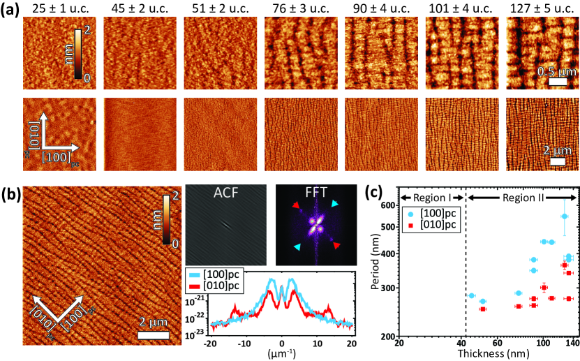
Atomic force microscopy (AFM) topography images obtained on the different samples reveal that as the PbTiO3 layer thickness increases, trenches develop at the surface of the SrRuO3 top layer in an organised pattern (Figure 1). For samples of 45 u.c. and below, this pattern is hardly visible and the top SrRuO3 is atomically flat. The pattern gets more pronounced and anisotropic with increasing PbTiO3 layer thickness, with long and deep trenches parallel to the [010]pc axis, and smaller trenches parallel to the [100]pc axis, while the surface roughness stays reasonably low, with root mean square (RMS) roughness values ranging from 157 to 393 pm over surfaces of 10 m 10 m. The pattern that we observe at the surface of the SrRuO3 top layer is comparable to what has been observed at the surface of PbTiO3 layers grown on DyScO3 substrates in Ref Nesterov-APL-2013 as a result of periodic ferroelastic domains.
To extract the period of the distortions visible on the surface of the samples, we calculate the autocorrelation function (ACF) of the topography image, and subsequently the fast Fourier transform (FFT) of the autocorrelation image, as shown in Figure 1(b) for the sample with the 90 u.c. thick PbTiO3 layer. As elaborated in Ref Nesterov-APL-2013 , this method is more sensitive to the periodic distortions of the surface of the sample than a direct FFT of the topography image. The results for the different samples are shown in Figure 1(c) and also reported in the concluding Figure 5. Once visible, the periods along both directions ([100]pc and [010]pc) increase as a function of PbTiO3 layer thickness, with the period along [100]pc being always larger than the period along [010]pc.
II.2 Periodic patterns in the PbTiO3 layers observed by x-ray diffraction
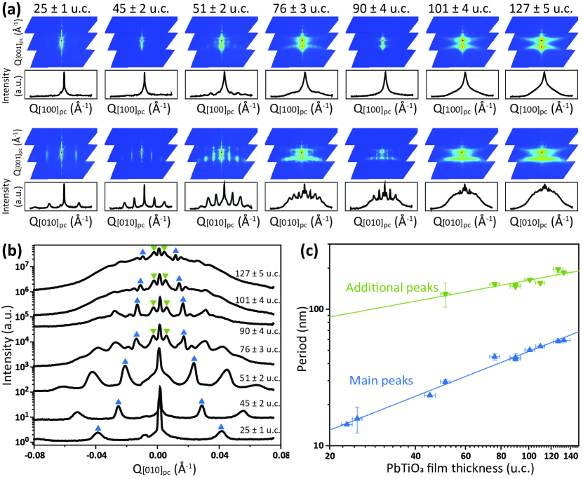
To relate this pattern observed at the surface of the SrRuO3 layer to the domain pattern in the PbTiO3 layers below, we used in-house x-ray diffraction to measure reciprocal space maps (RSM) of our different samples (Figure 2). For the thicker films, the butterfly shape - a signature of the -phase - can be recognised, with the high intensity peak of the substrate overlapping with the peak of the -domains and the peak of SrRuO3. The peak of the domains appears at a lower value. The butterfly wings arise from the tilts in the - and -domains Lee-AnnuRevMaterRes-2006 .
Comparing in Figure 2 the RSM obtained in the - plane (top row) and in the - plane (bottom row), we observe again an anisotropy between the two in-plane crystallographic axes and : periodic peaks are clearly visible along , whereas the peaks along are less well-defined and exhibit lower intensity. The position of these peaks was determined from intensity cuts at Å-1, corresponding to the region of the -domains, reported in Figure 2(b) (see blue arrows). From the position of these peaks, we extracted the periodicity - plotted in blue in Figure 2(c) as a function of the PbTiO3 film thickness. The blue line serves as a guide to the eye and is obtained by fitting the evolution of the period with film thickness using an exponential expression, . The best fit was obtained with , deviating from the Kittel law Landau-book-1992 ; Kittel-PR-1946 ; Mitsui-PR-1953 ; Roitburd-PSSA-1976 ; Pompe-JAP-1993 ; Pertsev-JAP-1995 where should be equal to (see Section III for a discussion regarding this deviation from the Kittel law).
Upon further analysis of the periodic peaks appearing in the RSM, we note in Figure 2(b) that additional peaks appear for the thicker films (see down-facing green triangles). These additional peaks correspond to larger periods, as reported in Figure 2(c) in green. This time, the fit gives , much closer to what one would expect from the Kittel law. For comparison, we analysed a 90 u.c PbTiO3 sample without the top SrRuO3 electrode using piezo-response force microscopy measurements. We observed that in addition to the domains, the out-of-plane polarisation arranges into larger regions alternating between up and down polarisation, forming superdomains (see discussion in Supporting Information Section S1 and in Ref. Tovaglieri-ToBeSubmitted-2023 ). The period of these superdomains matches with the value obtained from the additional peak in the RSM, confirming that the additional peaks come from the arrangement of the out-of-plane polarisation in superdomains. These additional peaks appear only for samples with a PbTiO3 layer thicker than 45 u.c., which is also the thickness above which the pattern starts to appear in the topography of the surface layer, as observed by AFM.
II.3 Tilts in - and -domains observed by synchrotron x-ray nanodiffraction
The 90 u.c. thick PbTiO3 layer sample was also analysed using scanning x-ray nanodiffraction microscopy (SXDM). This technique allows us to measure raster scans of local 3D-RSMs, with a spatial resolution determined by the focused x-ray beam size Hadjimichael-PRL-2018 , here full width at half maximum (FWHM). The output of an SXDM map is thus the diffracted intensity as a function of three reciprocal space coordinates (, , ), and two direct space coordinates (, and ) (Figure 3).
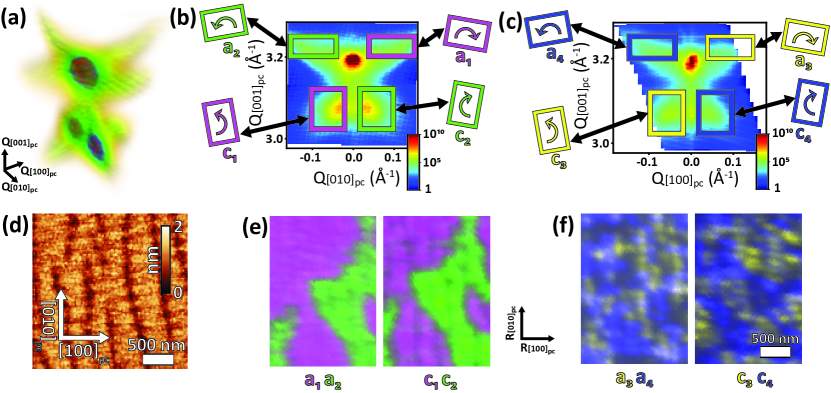
The average 3D-RSM obtained by summing over all sample positions is shown in Figure 3(a). The projections along and are shown in Figure 3(b-c). This RSM displays the “butterfly” shape characteristic of the phase already evident in Figure 2. Compared to Figure 2 however, in Figure 3(a-c) no satellites are present: because the domain period is comparable to the nanofocused beam size in a local 3D-RSM, the number of coherently illuminated periods is insufficient to give rise to the constructive interference that generates the satellites. The coloured boxes in Figure 3(b-c) each define a region of interest (ROI) corresponding to an or domain tilted in one of the four directions.
The sum of the intensity scattered within each ROI is computed for each local RSM and plotted as a function of in Figure 3(e-f). Here, each plot is labelled with the domain type and colour of the respective ROI, allowing us to map the presence or absence of the different domains. Note that due to their small size, it is clusters, or “bundles” of domains rather than individual ones that are visible. By comparing the intensity maps to the topography of the sample displayed at the same scale in Figure 3(d), one sees that the contrast is comparable, showing that the pattern observed in the topography of the SrRuO3 top layer is related to the arrangement of the domains in the PbTiO3 layer below.
Comparing the and domain maps in Figure 3(e-f), we see a clear correlation between the spatial distribution of different tilts: the spatial distribution of domains matches that of the domains (pink), the of the (green), the of the (yellow) and the of the (blue). Such pairing is to be expected given the crystallography of twins Speck1995 . More interestingly, and pairs appear to further aggregate at a larger scale into homogeneous areas, forming superdomains compatible with the observations in Figure 2 and Figure S1.
II.4 Domain patterns in PbTiO3 layers observed by transmission electron microscopy
A more direct way to image the domain structure is the use of cross-sectional scanning electron microscopy (STEM) (Figure 4). Atomically resolved high angle annular dark field (HAADF)-STEM imaging allows us to observe the lattice and atomic displacements at the atomic level. The samples were cut and prepared for the STEM measurement so as to obtain slices in the plane defined by the [010]pc (horizontal direction) and [001]pc (vertical direction) axes of DyScO3, imaging along the [100]pc zone-axis. In the 90 u.c. thick PbTiO3 in Figure 4, the -domains are clearly visible as very narrow domains separated from the larger -domains by domain walls in the and planes.
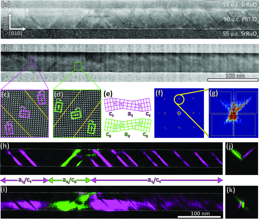
Focusing on a region with the domain walls in the planes (Figure 4(c)), we observe the tilted and -domains, corresponding to an -domain surrounded by -domains. In the case of domain walls in the planes (Figure 4(d)), we observe an -domain surrounded by -domains. These correspond to the and pairing observed in the nanodiffraction data (Figure 3).
Interestingly, in these two different regions, the polarisation in the -domains is always oriented down (in the [001]pc direction), while the polarisation in the -domains is always oriented to the right (in the [010]pc direction).
At a larger scale, the periodic pattern is directly visible in real space and the period can be estimated by taking the FFT of the image, as shown in Figure 4(f). Looking at the (001)pc Bragg spot in the obtained reciprocal space map (Figure 4(g)), one can see the superstructure with a periodicity corresponding to 40-45 nm, in perfect agreement with the values obtained from the RSM (see Figure 5 for the comparison between values obtained by the different techniques).
In Figure 4(g), one also recognizes the butterfly shape as observed by XRD and nanodiffraction. By selecting different regions of interest, it is then possible to reconstruct the direct space images in Figure 4(h-i) revealing the mapping of the and -domains ( and in pink, and in green). Although the reconstructed image is sharper for the -domains (Figure 4(h)) than for the -domains (Figure 4(i)), it allows us to confirm at a local scale and with direct imaging the result obtained by nanodiffraction: the and -domains organize themselves, not only in pairs, but in larger regions composed of several / pairs alternating with larger regions composed of several / pairs, forming superdomain structures.
III Discussion
The different periods observed in this work along [010]pc are summarised in Fig. 5(d): from the AFM topography, the RSM, and the STEM images. From this Figure, we see a good match between the values obtained by STEM and RSM. We also see that two different regions can be defined: region I where no pattern is visible in the topography for the thinner PbTiO3 films (45 u.c. and lower), and region II where the topography displays tilts and trenches, and where additional peaks appear in the RSM for the thicker PbTiO3 films (50 u.c. and higher).
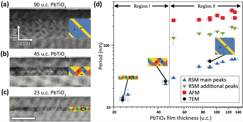
The STEM measurements show that the sample in region II has a clear -phase domain structure (Fig. 5(a) - 904 u.c. thick PbTiO3), while the two samples measured in region I show a more complex domain pattern (Fig. 5(b) - 452 u.c. and (c) - 231 u.c. thick PbTiO3 layers). In these images, domain walls are clearly visible in the PbTiO3 layers, forming an pattern for the thicker PbTiO3 layer and transforming into a flux-closure like pattern for the thinner PbTiO3 layers, sharing similarities to what was observed in PbTiO3/SrTiO3 heterostructures on GdScO3 Tang-Science-2015 .
By performing FFT filtering for these three films, as was done for the 90 u.c. thick PbTiO3 sample in Figure 4, we extracted the periodicity of these different domain configurations and found 40-45 nm for the 90 u.c. thick PbTiO3, 25-30 nm for the 45 u.c. thick PbTiO3, and 16 nm for the 23 u.c. thick PbTiO3, in perfect agreement with the values obtained from the RSM (see Figure 5(d) - black dots).
Nanodiffraction measurements allowed us to spatially resolve the pattern in the sample with 90 u.c. thick PbTiO3 and demonstrated the coupling of the tilts of the - and -domains, as also observed by STEM.
Nanodiffraction also demonstrated the organisation of these domains at a larger scale. From the STEM measurements combined with the spatially resolved XRD measurements, we conclude that in the -phase, the -domains organise in “superdomains”, i.e. regions composed of either , , , or domains. This gives rise to an additional periodicity that can be detected as additional peaks in the RSM. From the PFM measurements in a sample without the top SrRuO3 electrode, we relate these additional periodic peaks to the 180∘ ferroelectric domains (). Although we could not confirm it directly, one possibility is that these domains correspond to the superdomains observed with different tilts.
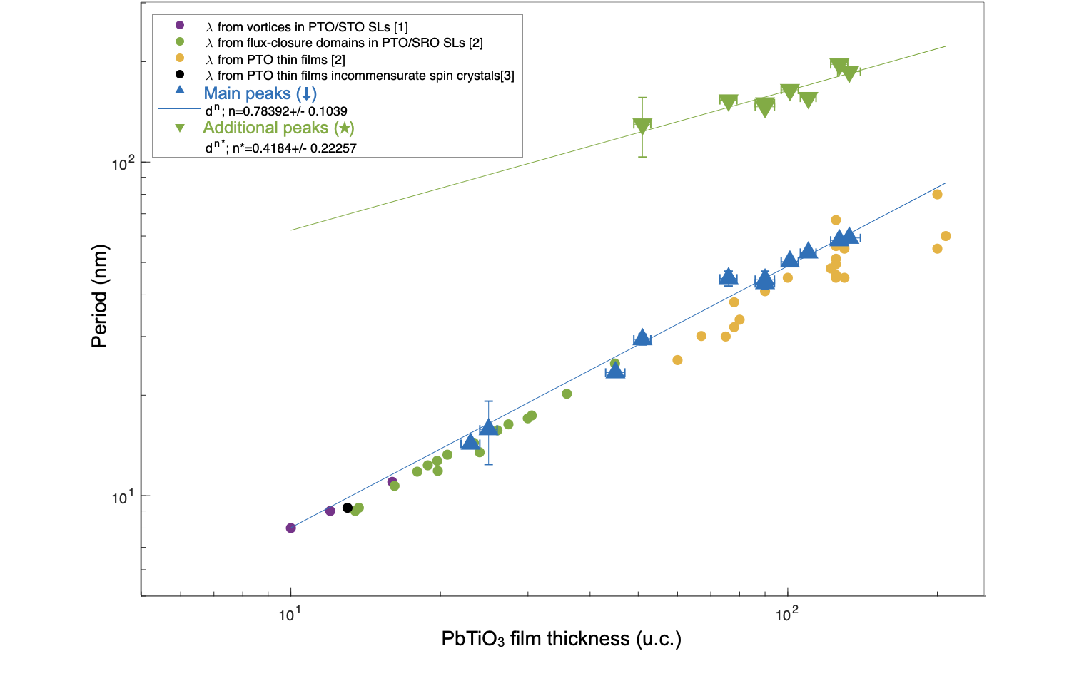
Looking at the evolution of the periods as a function of film thickness, we observe that the period of the ferroelastic domain structure in the PbTiO3 layers decreases with decreasing film thickness as with . This is very close to the value obtained by Nesterov et al. Nesterov-APL-2013 (). It also compares well with the results obtained in different works (see Supporting Information, Section S2).
When considering the energetics at play in ferroelastic domains in epitaxial ferroelectric and ferroelastic films, Pertsev Pertsev-JAP-1995 showed that the dependence of the equilibrium domain period on film thickness varies from linear to the usual square root law at very large film thickness, as the domain wall energy density varies with film thickness. At very low thicknesses, the domain size can even increase as the film thickness is reduced Pertsev-JAP-1995 ; Kopal-Ferroelectrics-1997 ; Huang-JAP-2013 . Although we did not observe such a turnover of domain size for our samples with lower film thickness, we believe this mechanism is at play in our materials and could explain the existence of the two different regions. In region II, the samples are in the -phase with the period expected for this epitaxial strain. They form superdomains, probably controlled by the domain configuration determined by the screening of the depolarisation field and electrostatic boundary conditions. Both of these patterns in region II have a period that decreases with film thickness, following the Kittel law for the superdomains, and following an intermediate behavior between Kittel’s square-root law and Pertsev’s linear law for the ferroelastic -domains. In this region, the change between and can easily take place on each side of the -domains, without additional cost of formation of 180∘ domain walls. However, as the film thickness is reduced further, we enter in region I into a regime where the -domain size should increase exponentially as the film thickness is reduced, going towards a monodomain state. However, the cost of the depolarisation field is still increasing and needs to be compensated by domains. In this regime, many 180∘ domain walls would then have to be created, at a large energy cost. We observe that instead of this configuration, the domains end up in a more complex polarisation texture, similar to flux-closure pattern, with a period following the behavior of the -domain pattern at larger thickness, and without any additional peaks or superdomain structure. This new complex polarisation pattern appearing at lower thickness is thus the best compromise between the behavior expected for ferroelectric vs. ferroelastic domains, reducing the cost of strain and depolarisation field at the same time. This explains why in this regime, it is possible to observe very complex patterns such as flux-closure Tang-Science-2015 ; Hadjimichael-NatMat-2021 , vortices Yadav2016 ; Shafer2018 ; Damodaran2017 , supercrystals Hadjimichael-NatMat-2021 and incommensurate spin (polarisation) structures Rusu-Nature-2022 , all with the period determined by the strain from the substrate and the layer thickness.
IV Conclusion
Our work demonstrates the presence of two regimes with different ferroelectric/ferroelastic domain configurations. For the smaller PbTiO3 thicknesses, the combination of the effect of strain and electrostatic boundary conditions gives rise to a complex domain configuration where flux-closure, vortices or supercrystal configurations can develop. For larger PbTiO3 thicknesses, the -phase induced by epitaxial strain is recovered, with large superdomains appearing to screen the depolarisation field. The large structural distortions associated with the ferroelastic domains propagate through the top SrRuO3 layer, creating a modulated structure that extends beyond the ferroelectric layer thickness, allowing domain engineering in the top SrRuO3 electrode Lichtensteiger-SRO-ToBeSubmitted-2023 . These domain structures not only change the properties of the ferroelectric itself, but can also be used to change the properties of other materials through electrostatic and structural coupling.
V Experimental techniques
V.1 Sample growth
All the samples were deposited using our in-house constructed off-axis radio-frequency magnetron sputtering system, equipped with three different guns allowing the deposition of heterostructures and solid-solutions of high crystalline quality, composed of up to three different materials: PbTiO3, SrTiO3 and SrRuO3. PbTiO3 thin films are typically deposited around 560∘C and 580∘C, in 180 mTorr of a 20:29 O2/Ar mixture, at a power of 60 W, and using a Pb1.1TiO3 target with 10% excess of Pb to compensate for its volatility. SrRuO3 electrodes were deposited in situ from a stoichiometric target at 640∘C in 100 mTorr of O2/Ar mixture of ratio 3:60, at a power of 80 W. Huettinger PFG 300 RF power supplies are used in power control mode. The sample holder is grounded during deposition, but the sample surface is left floating.
V.2 Atomic force microscopy
Topography measurements were performed using a Digital Instrument Nanoscope Multimode DI4 with a Nanonis controller. Piezoresponse force microscopy measurements under ambient conditions to image the intrinsic domain patterns were performed on an Asylum Research Cypher or MFP-3D atomic force microscopes.
V.3 X-ray diffraction
In-house XRD measurements were performed using a Panalytical X’Pert diffractometer with Cu K radiation (1.5405980 Å) equipped with a 2-bounce Ge(220) monochromator and a triple axis detector in our laboratory in Geneva. The -2 scans were analysed using the InteractiveXRDFit software Lichtensteiger-JApllCryst-2018 . This XRD system is also equipped with a PIXcel1D detector, used for faster acquisition of the reciprocal space maps.
The 90 u.c. thick PbTiO3 layer sample was further analysed using scanning x-ray diffraction microscopy (SXDM) Hadjimichael-PRL-2018 on the ID01 beamline at the European Synchrotron Radiation Facility (ESRF) Leake2019 . An incident x-ray energy of 9.5 keV was selected using a Si(111) double crystal monochromator with resolution . A m-thick tungsten Fresnel zone plate with 300 m diameter and 20 nm outer zone width was used to focus the x-ray beam down to a spot size of approx. FWHM, as measured via a ptychography scan of a known reference object Leake2019 . The sample was placed at the diffraction condition and raster scanned relative to the focused beam in 25 nm steps over a area using a commercial piezo scanner. A two-dimensional MAXIPIX detector positioned approx. 0.4 m downstream of the sample stage was exposed for 12 ms at each sample position. The procedure was repeated at different incidence angles about the condition to obtain a 5-dimensional dataset describing the diffracted intensity as a function three reciprocal and two direct space dimensions, i.e. . We note that reaching the diffraction condition entails forming a 19∘ angle with the (00L) planes; since measurements were performed with x-ray beam parallel to , the direct space resolution is degraded along this direction, and features appear elongated parallel to it.
V.4 Scanning transmission electron microscopy
Cross-sectional lamella prepared by focus ion beam allow the imaging of domain structures by scanning transmission electron microscopy (STEM). Experiments were acquired on Nion Cs-corrected UltraSTEM200 at 100 kV operating voltage. A convergence angle of 30 mrad was used to allow high-resolution atomic imaging with a typical spatial resolution of 1 Å. Three imaging detectors in the STEM are used to simultaneously obtain bright field (BF), annular bright field (ABF) or medium angle annular dark field (MAADF), and high angle annular dark field (HAADF) images.
For ABF-MAADF imaging, the inner-outer angles can be continuously adjusted between 10-20 to 60-120 mrad. Most ABF images were collected with 15-30 mrad and MAADF images with 40-80 mrad angular ranges.
We determine the periodicity of the superstructures in the PbTiO3 layer by measuring the distances between the additional reciprocal space spots obtained after FFT. The accuracy of the measurement was estimated by considering the diffraction spot extension as the lower and upper limit for the superstructure length estimation.
VI Data availability
The data that support the findings of this study are available at Yareta (DOI).
VII Acknowlegements
The authors thank Kumara Cordero-Edwards and Christian Weymann for support and discussions.
This work was supported by Division II of the Swiss National Science Foundation under project 200021_200636. STEM experiments were supported by the EU Horizon research and innovation program under grant agreement ID 823717-ESTEEM3. M.H. acknowledges funding from the SNSF Scientific Exchanges Scheme (Grant Number IZSEZ0_212990).
VIII Author contributions
C.L, M.H., P.P., A.G. and J.M.T. designed the experiment. C.L., M.H. and L.T. grew the samples and conducted the AFM and XRD measurements and analysis. E.Z. conducted the synchrotron x-ray nanodiffraction measurements and analysis. C.-P.S. and A.G. conducted the STEM measurements and analysis. I.G. performed additional STEM analysis. C.L., M.H., I.G. and P.P. wrote the manuscript with contributions from all authors. All authors discussed the experimental results and models, commented on the manuscript, and agreed on its final version.
IX Bibliography
References
- (1) Pertsev, N. A., Zembilgotov, A. G. & Tagantsev, A. K. Effect of Mechanical Boundary Conditions on Phase Diagrams of Epitaxial Ferroelectric Thin Films. Physical Review Letters 80, 1988–1991 (1998).
- (2) Pertsev, N. A. & Koukhar, V. G. Polarization instability in polydomain ferroelectric epitaxial thin films and the formation of heterophase structures. Physical Review Letters (2000).
- (3) Koukhar, V. G., Pertsev, N. A. & Waser, R. Thermodynamic theory of epitaxial ferroelectric thin films with dense domain structures. Physical Review B - Condensed Matter and Materials Physics 64, 1–15 (2001). eprint 0102460.
- (4) Li, Y. L., Hu, S. Y., Liu, Z. K. & Chen, L. Q. Phase-field model of domain structures in ferroelectric thin films. Applied Physics Letters 78, 3878–3880 (2001).
- (5) Jiang, Z. et al. Strain-induced control of domain wall morphology in ultrathin PbTiO3 films. Physical Review B - Condensed Matter and Materials Physics 89, 35–37 (2014).
- (6) Chapman, J. B., Kimmel, A. V. & Duffy, D. M. Novel high-temperature ferroelectric domain morphology in PbTiO3 ultrathin films. Physical Chemistry Chemical Physics 19, 4243–4250 (2017).
- (7) Schlom, D. G. et al. Strain Tuning of Ferroelectric Thin Films. Annual Review of Materials Research 37, 589–626 (2007).
- (8) Yadav, A. K. et al. Observation of polar vortices in oxide superlattices. Nature 530, 198–201 (2016). URL http://dx.doi.org/10.1038/nature16463.
- (9) Shafer, P. et al. Emergent chirality in the electric polarization texture of titanate superlattices. Proceedings of the National Academy of Sciences of the United States of America 115, 915–920 (2018).
- (10) Stoica, V. A. et al. Optical creation of a supercrystal with three-dimensional nanoscale periodicity. Nature Materials 18, 377–383 (2019).
- (11) Hadjimichael, M. Ferroelectric domains in lead titanate heterostructures. Ph.D. thesis, University College London (2019).
- (12) Hadjimichael, M. et al. Metal–ferroelectric supercrystals with periodically curved metallic layers. Nature Materials 20, 495—-502 (2021).
- (13) Rusu, D. et al. Ferroelectric incommensurate spin crystals. Nature 602, 240–244 (2022).
- (14) Gonçalves, M. A., Escorihuela-Sayalero, C., Garca-Fernández, P., Junquera, J. & Íñiguez, J. Theoretical guidelines to create and tune electric skyrmion bubbles. Science Advances 5, 1–6 (2019).
- (15) Das, S. et al. Observation of room-temperature polar skyrmions. Nature 568, 368–372 (2019).
- (16) Wang, Y. J. et al. Polar meron lattice in strained oxide ferroelectrics. Nature Materials (2020).
- (17) Íñiguez, J., Zubko, P., Luk’yanchuk, I. & Cano, A. Ferroelectric negative capacitance. Nature Reviews Materials 4 (2019).
- (18) Damodaran, A. R. et al. Phase coexistence and electric-field control of toroidal order in oxide superlattices. Nature Materials 16, 1003–1009 (2017).
- (19) Shirane, G., Pepinsky, R. & Frazer, B. C. X-ray and neutron diffraction study of ferroelectric PbTiO3. Acta Crystallographica 9, 131–140 (1956). URL https://doi.org/10.1107/S0365110X56000309.
- (20) Veličkov, B., Kahlenberg, V., Bertram, R. & Bernhagen, M. Crystal chemistry of GdScO3, DyScO3, SmScO3 and NdScO3. Zeitschrift fur Kristallographie 222, 466–473 (2007).
- (21) “” subscript refers to the pseudocubic unit cell, while “” is used to refer to the orthorhombic unit cell.
- (22) Catalan, G. et al. Flexoelectric rotation of polarization in ferroelectric thin films. Nature Materials 10, 963–967 (2011). URL http://dx.doi.org/10.1038/nmat3141.
- (23) Nesterov, O. et al. Thickness scaling of ferroelastic domains in PbTiO3 films on DyScO3. Applied Physics Letters 103, 142901 (2013).
- (24) Highland, M. J. et al. Interfacial charge and strain effects on the ferroelectric behavior of epitaxial (001) PbTiO3 films on (110) DyScO3 substrates. Applied Physics Letters 104, 1–4 (2014).
- (25) Junquera, J. & Ghosez, P. Critical thickness for ferroelectricity in perovskite ultrathin films. Nature 422, 506–509 (2003).
- (26) Aguado-Puente, P. & Junquera, J. Ferromagneticlike closure domains in ferroelectric ultrathin films: First-principles simulations. Physical Review Letters 100, 1–4 (2008).
- (27) Stengel, M., Vanderbilt, D. & Spaldin, N. A. Enhancement of ferroelectricity at metal-oxide interfaces. Nat. Mater. 8, 392–397 (2009).
- (28) Li, S. et al. Periodic arrays of flux-closure domains in ferroelectric thin films with oxide electrodes. Applied Physics Letters 111 (2017).
- (29) Hadjimichael, M., Li, Y., Yedra, L., Dkhil, B. & Zubko, P. Domain structure and dielectric properties of metal-ferroelectric superlattices with asymmetric interfaces. Physical Review Materials 4, 1–8 (2020).
- (30) Eom, C. et al. Single-Crystal Epitaxial Thin Films of the Isotropic Metallic Oxides Sr1-xCaxRuO3 (0 x 1). Science 258, 1766–1769 (1992).
- (31) Randall, J. J. & Ward, R. The Preparation of Some Ternary Oxides of the Platinum Metals. Journal of the American Chemical Society 81, 2629–2631 (1959).
- (32) Tang, Y. L. et al. Observation of a periodic array of flux-closure quadrants in strained ferroelectric PbTiO3 films. Science 348, 547–551 (2015).
- (33) Li, S. et al. Evolution of flux-closure domain arrays in oxide multilayers with misfit strain. Acta Materialia 171, 176–183 (2019).
- (34) Nečas, D. & Klapetek, P. Gwyddion: An open-source software for SPM data analysis. Central European Journal of Physics 10, 181–188 (2012).
- (35) Lee, K. & Baik, S. Ferroelastic domain structure and switching in epitaxial ferroelectric thin films. Annual Review of Materials Research 36, 81–116 (2006).
- (36) Landau, L., Lifshitz, E. & Lifšic, E. M. On the theory of the dispersion of magnetic permeability in ferromagnetic bodies (Pergamon Press, Oxford, 1992).
- (37) Kittel, C. Theory of the structure of ferromagnetic domains in films and small particles. Physical Review 70, 965–971 (1946).
- (38) Mitsui, T. & Furuichi, J. Domain structure of rochelle salt and KH2PO4. Physical Review 90, 193–202 (1953).
- (39) Roitburd, A. L. Equilibrium structure of epitaxial layers. Physica Status Solidi (a) 37, 329–339 (1976).
- (40) Pompe, W., Gong, X., Suo, Z. & Speck, J. S. Elastic energy release due to domain formation in the strained epitaxy of ferroelectric and ferroelastic films. Journal of Applied Physics 74, 6012–6019 (1993).
- (41) Pertsev, N. A. & Zembilgotov, A. G. Energetics and geometry of 90∘ domain structures in epitaxial ferroelectric and ferroelastic films. Journal of Applied Physics 78, 6170–6180 (1995).
- (42) Tovaglieri, L. & et al. Ferroelastic/ferroelectric superdomains pattern in epitaxially strained PbTiO3 heterostructures observed by Piezo-response Force Microscopy. To be submitted (2023).
- (43) Hadjimichael, M., Zatterin, E., Fernandez-Peña, S., Leake, S. J. & Zubko, P. Domain Wall Orientations in Ferroelectric Superlattices Probed with Synchrotron X-Ray Diffraction. Physical Review Letters 120, 1–6 (2018). eprint 1801.01772.
- (44) Speck, J. S., Daykin, A. C., Seifert, A., Romanov, A. E. & Pompe, W. Domain configurations due to multiple misfit relaxation mechanisms in epitaxial ferroelectric thin films. III. Interfacial defects and domain misorientations. Journal of Applied Physics 78, 1696–1706 (1995).
- (45) Kopal, A., Bahnik, T. & Fousek, J. Domain formation in thin ferroelectric films: The role of depolarization energy. Ferroelectrics 202, 267–274 (1997).
- (46) Huang, C. W., Chen, Z. H. & Chen, L. Thickness-dependent evolutions of domain configuration and size in ferroelectric and ferroelectric-ferroelastic films. Journal of Applied Physics 113 (2013).
- (47) Lichtensteiger, C. & et al. Nanoscale domain engineering in SrRuO3 thin films. To be submitted (2023).
- (48) Lichtensteiger, C. InteractiveXRDfit: A new tool to simulate and fit X-ray diffractograms of oxide thin films and heterostructures. Journal of Applied Crystallography 51, 1745–1751 (2018).
- (49) Leake, S. J. et al. The nanodiffraction beamline ID01/ESRF: A microscope for imaging strain and structure. Journal of Synchrotron Radiation 26, 571–584 (2019).
Supplementary Materials
S1 Observation of superdomains in a sample without the top SrRuO3 electrode
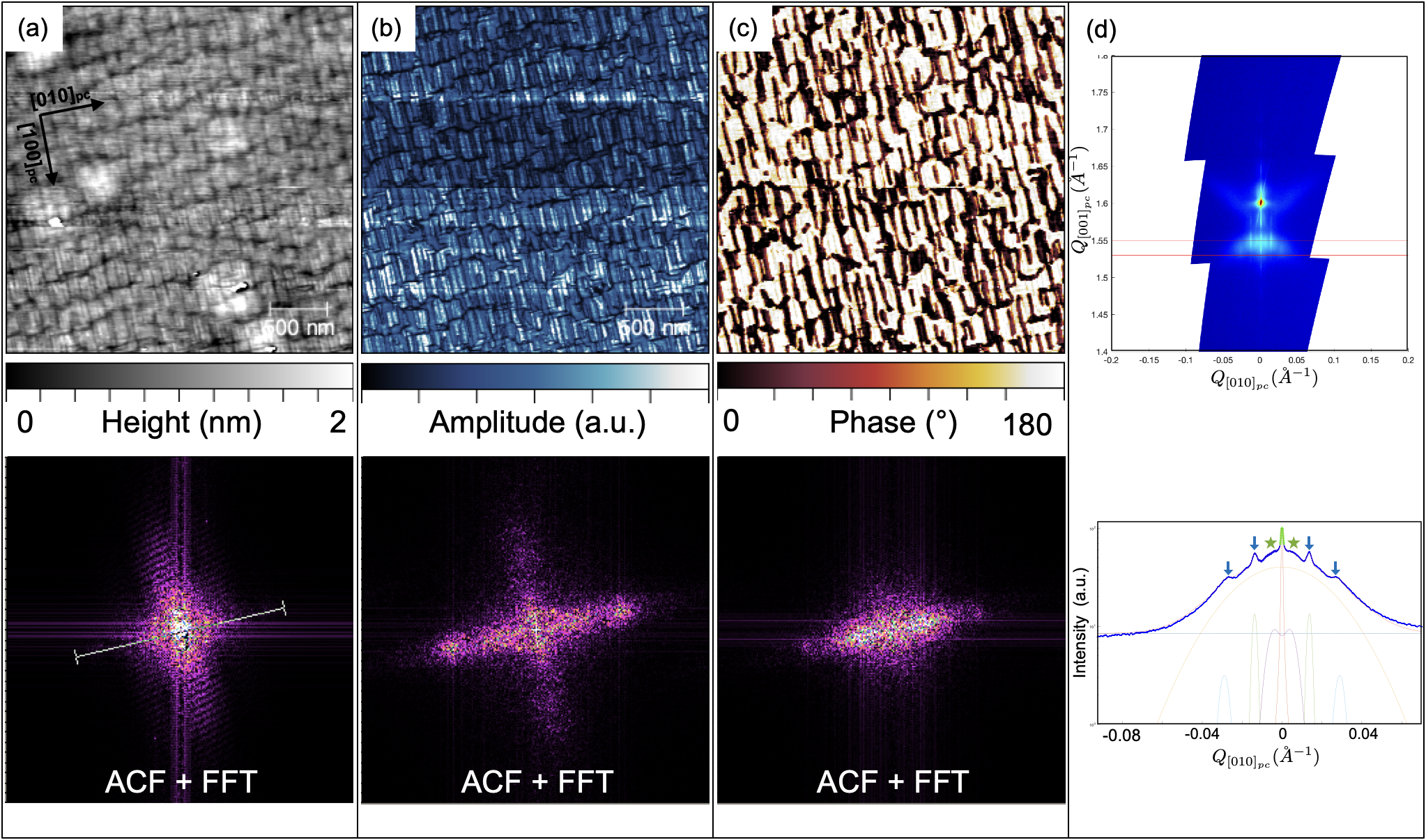
To allow for direct visualisation of domain configuration using piezo-response force microscopy (PFM), we also grew a sample without the top SrRuO3 electrode: 90 4 u.c. PbTiO3 on 53 3 u.c. SrRuO3 on DyScO3 substrate. In Figure S1, we show the topography image (a), where we can observe the trenches at the top of the PbTiO3 layer, very similar to what we observe in the sample of the same PbTiO3 thickness with the top SrRuO3 electrode. The anisotropic pattern has a period of 266 nm along [100]pc and 46 nm along [010]pc (ACF+FFT analysis of the topography image). In (b) we show the PFM vertical amplitude, where we see dark lines corresponding to 180∘ domain walls and/or -domains. ACF+FFT analysis of the amplitude image gives a period of 280 nm along [100]pc and 48 nm along [010]pc, following the values obtained on the topography image. In (c) we show the PFM vertical phase, with a clear signature of superdomains where the domains organise in regions where the out-of-plane polarisation points up, alternating with regions where the out-of-plane polarisation points down. From the ACF+FFT analysis of this PFM vertical phase image, we extract a period of 1175 150 nm along [100]pc and 145 6 nm along [010]pc for the superdomains. In (d), we show the RSM obtained around (001)pc in the plane, showing the typical butterfly shape of the -phase and the additional peaks of the periodic pattern. From the cut at Å-1 (-domains), we extract the intensity profile showing the periodic peaks indicating a periodicity of 45 2 nm. This value matches perfectly with the values obtained from the analysis of the topography and amplitude images. From the intensity cut in the RSM, we also see the shoulders (indicated by green stars in Figure S1(d)), corresponding to an additional period of 150 2 nm. This value corresponds to that obtained from the analysis of the PFM phase image, confirming that the additional peaks come from the arrangement of the out-of-plane polarisation in superdomains.
S2 Deviation from Kittel law: Comparison with ferroelastic and flux-closure domains in other PbTiO3 thin films and superlattices on DyScO3
Comparing to other periods found in the literature to our results (Figure S2), we see that the trend we observe is universally followed: the period in the PbTiO3 layers is the same in all the different heterostructures and is fixed by the epitaxial strain imposed by the DyScO3 substrate, whether in thin films or superlattices, forming -domains or more complex polarisation textures like flux-closure, vortices, supercrystals or incommensurate spin crystals.
