Radiative suppression of exciton-exciton annihilation in a two-dimensional semiconductor
Two-dimensional (2D) semiconductors possess strongly bound excitons, opening novel opportunities for engineering light-matter interaction at the nanoscale. However, their in-plane confinement leads to large non-radiative exciton-exciton annihilation (EEA) processes, setting a fundamental limit for their photonic applications. In this work, we demonstrate suppression of EEA via enhancement of light-matter interaction in hybrid 2D semiconductor-dielectric nanophotonic platforms, by coupling excitons in WS2 monolayers with optical Mie resonances in dielectric nanoantennas. The hybrid system reaches an intermediate light-matter coupling regime, with photoluminescence enhancement factors up to 102. Probing the exciton ultrafast dynamics reveal suppressed EEA for coupled excitons, even under high exciton densities 1012 cm-2. We extract EEA coefficients in the order of 10-3, compared to 10-2 for uncoupled monolayers, as well as absorption enhancement of 3.9 and a Purcell factor of 4.5. Our results highlight engineering the photonic environment as a route to achieve higher quantum efficiencies for low-power hybrid devices, and larger exciton densities, towards strongly correlated excitonic phases in 2D semiconductors.
The Auger-Meitner effect in semiconductor is a scattering process where two charge carriers collide, resulting in a non-radiative decay via a mutual exchange of momentum [1]. It represents a major loss channel in optoelectronic devices, posing a fundamental limit on their quantum efficiency under high carrier densities. In particular, for low-dimensional semiconductors, quantum confinement restricts the momentum conservation rules of carriers and allows for stable Coulomb bound electron-hole pairs, or excitons. These can scatter via the mutual dipole-dipole interaction, in the form of exciton-exciton annihilation (EEA), yielding large scattering rates compared to bulk materials, as observed in quantum dots [2], quantum wells [3] and carbon nanotubes [4]. In the case of two-dimensional (2D) semiconductors, control and suppression of EEA is fundamental to unlock their potential for applications [5]. Transition metal dichalcogenides (TMDCs) emerged as the most promising family of atomically thin semiconductors for photonic applications [6]. Owing to large exciton binding energies above 200 meV, TMDCs optical properties are dominated by their excitonic response up to room temperature [7], while at cryogenic temperatures TMDCs exhibit appealing properties, such as the presence of many body excitonic species [8] or single photon emitters [9]. However, excitons in 2D TMDCs possess large Bohr radii, in the order of 1 nm, increasing their mutual interaction ranges and resulting in large EEA coefficients, reaching values larger than in any other semiconducting material [5]. EEA is thus observed even at relatively low exciton populations, setting a fundamental limit for the generation of high exciton densities in 2D semiconductors. Experimental techniques, such as time resolved luminescence or ultrafast transient absorption spectroscopy, have been employed to study EEA processes in atomically thin and bulk TMDCs [10, 11, 12, 13]. EEA effect introduces a drastic change the exciton dynamics, observed as a fast recombination process, in the order of few picoseconds, which follows a quadratic dependence with the generated exciton population [11]. Recent works explored various approaches for suppressing EEA processes. For instance, by encapsulating TMDCs monolayers in hexagonal boron nitride [14], extracting excess free carriers [15], or the simultaneous application of strain and a gate voltage [16]. Notably, EEA processes in 2D semiconductors can also be harnessed to provide unexpected effects, for instance in generation of upconverted photoluminescence [17, 18], increased photocurrents [19], and creation of negative mass excitons [20].
An alternative approach to overcome the limitations imposed by EEA is offered by the integration of 2D semiconductors in nanophotonic architectures, tailoring the dielectric environment and the local density of states experienced by 2D confined excitons. The ability of 2D TMDCs to conform to underlying nanophotonic structures, and couple to the strong near field at their surfaces, have been demonstrated to enhance light-matter interaction in excitons [21, 22, 23, 24, 25] and single photon emitters [26, 27], making them a promising material for hybrid nanophotonic devices. Resonant dielectric optical nanoantennas recently emerged as a novel platform to overcome the intrinsic losses of metal based plasmonic counterparts, while providing a new toolbox to tailor light-matter interaction at the nanoscale [28]. By sustaining the presence of both electric and magnetic type of optical resonances, multimodal interference of electromagnetic Mie modes in a single dielectric nanoantenna opens to higher degrees of control on light-matter interaction, from unidirectional scattering effects [29] to suppression of far field emission [30]. This approach can be further extended to arrays of nanoantennas, or metasurfaces, for the manipulation of phase and amplitude of light in sub-wavelength dimensions and the physics of bound states in the continuum [31].
In this work, we demonstrate the suppression of EEA processes via radiative rate enhancement, by coupling excitons in WS2 monolayers with Mie resonances of gallium phosphide (GaP) dielectric nanoantennas [32]. We show that the hybrid 2D semiconductor-dielectric nanoantenna system reaches an intermediate light-matter coupling regime and observe photoluminescence (PL) enhancement factors above 102 compared to uncoupled monolayers, as well as a reduction of the PL lifetime, a signature of spontaneous emission rate enhancement. We then probe the exciton dynamics with ultrafast transient absorption spectroscopy. For uncoupled excitons, we observe the expected onset of non-radiative EEA as a fast recombination process in their dynamics [11]. On the contrary, excitons coupled to the near fields of GaP nanoantennas exhibit negligible changes in their dynamics over a broad range of excitation powers. We show this is the combined effect of the enhanced absorption rate via near field coupling, and increased spontaneous emission rate via the Purcell effect, leading to excitons having higher probability to recombine radiatively, rather than experiencing diffusion and non-radiative processes. In the framework of a rate equation model, we extract the values of the EEA coefficient () and found one order of magnitude lower values for WS2 excitons coupled to resonant nanoantennas, as compared to uncoupled excitons on glass substrate. Moreover, by comparing their ultrafast dynamics, we extract an enhanced absorption rate () of 3.9 and a Purcell factor () of 4.5. This behaviour goes against the phenomenological law of decreasing EEA coefficients with longer exciton lifetimes [33], highlighting enhanced light-matter interaction as a key for the suppression of EEA processes in 2D semiconductors. Our results demonstrate hybrid nanophotonics architectures as an attractive platform to engineer light-matter coupling with 2D materials and provide a route to overcome fundamental limitations induced by exciton scattering, enabling application of 2D semiconductors in photonic devices.
Results
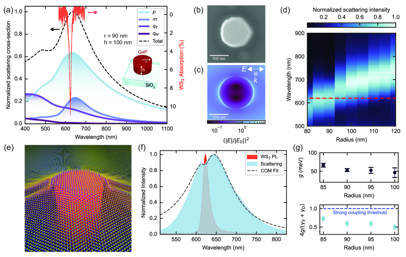
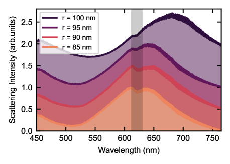
Intermediate light-matter coupling regime in hybrid 2D semiconductor-dielectric nanoantennas We select the geometry of the GaP nanoantenna to maximize the spectral overlap between the magnetic and electric dipolar Mie resonances and excitons in WS2 monolayers. Figure 1a shows the finite-difference time-domain (FDTD) numerical simulation of the scattering spectrum for a single GaP nanoantenna on a SiO2 glass substrate (dashed black line), with a radius of 90 nm and height of 100 nm. The red curve represents the experimental optical absorption of the 1s-exciton state in a monolayer WS2 on SiO2 substrate, also referred to as A exciton in literature [7]. The scattering cross-section can be described with a multipolar expansion of the induced electromagnetic currents [31], quantifying the individual contributions from the optical Mie resonances, respectively the electrical () and magnetic () dipoles, and the electrical () and magnetic () quadrupoles. We fabricated an array of optical nanoantennas by depositing thermally grown amorphous GaP on top of fused silica substrates, and patterned the thin film with conventional electron beam lithography and reactive ion etching techniques (see Methods for details). Figure 1b shows a top view electron microscope image of a fabricated cylindrical GaP nanoantenna on SiO2 substrate. At its surface, the nanoantenna confines and enhances the electromagnetic field intensity, , defined as the ratio between the electric field amplitude of the scattered field by the antenna () and the normally incident field (). Figure 1c shows the numerical simulations for the enhanced near field region, recorded at the top surface of a single GaP nanoantenna. By tuning the radial dimension of the nanoantennas, we tailor the wavelength of the Mie resonances to match with the WS2 exciton wavelength. Figure 1d shows the darkfield scattering spectra of the fabricated GaP nanoantennas array, in good agreement with the numerical simulations in Figure 1a. As expected from Mie theory, increasing the resonator size shifts the Mie resonances to lower energies, crossing the WS2 exciton energy (dashed red line in Figure 1d).
To probe the coupled system, we transfer the WS2 monolayer on top of the nanoantenna array with an all-dry transfer technique (see Methods and Supplementary Note I). Figure 1e displays an illustration of a monolayer WS2 transferred on top of a cylindric GaP dielectric nanoantenna on a glass substrate. The atomically thin layer stretches on top of the nanoantenna, in close proximity with the enhanced near field region. Figure 1f shows the WS2 PL emission and the dark field scattering spectra of a hybrid nanoantenna covered with a WS2 monolayer. The scattering spectrum is modified by the presence of the atomically thin layer, in the form of a dip in correspondence to the PL exciton peak of the coupled WS2 monolayer (see also Supplementary Note II), indicating an enhanced absorption via the resonant coupling between excitons and Mie resonances [34]. We treat the nanoantennas optical resonances and WS2 excitons as damped coupled oscillators, and fit the scattering spectrum of the hybrid system with a coupled oscillator model (COM) in the form [34]:
| (1) |
where and are the exciton and antenna dipolar resonance linewidths, respectively, and the exciton and antenna resonance frequencies, is a scaling constant, and the coupling strength constant. In Figure 1g we plot the extracted values of (top panel) for WS2 coupled to different antennas with radius ranging from 85 nm to 100 nm. We found values in the range of 50-60 meV, comparable with similar hybrid architectures based on plasmonic nanoantennas [25]. We then compare the extracted values of with the strong coupling condition satisfying that [34] (Figure 1g, bottom panel). Due to the variation in linewidth of the fabricated antennas and the strain affecting the exciton resonance linewidth, we define a normalized value of the strong coupling condition as . For all the hybrid systems studied, we obtain values where , confirming the increased light-matter interaction of WS2 excitons coupled to optical Mie resonances, and placing our hybrid 2D semiconductor-dielectric system in the intermediate light-matter coupling regime.
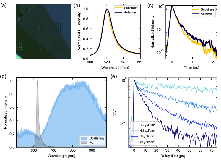
Radiative rate enhancement in coupled WS2 excitons We further investigate the PL properties of coupled WS2 excitons by means of steady state and time resolved optical spectroscopy. Figure 2a shows the PL map of the monolayer transferred on top of a resonant GaP nanoantennas array. The sample is excited with a 530 nm, 140 fs pulsed laser, with repetition rate of 80 MHz and average power of 14 nW. We scan the sample with piezoelectric stages, and record the PL intensity with an avalanche photodetector (see Methods). We observe more than one order of magnitude enhancement of PL emission when the monolayer is placed on top of the nanoantennas, owing to the interplay of enhanced light emission and absorption rates of the coupled nanophotonic system [21]. Figure 2b shows the spectra of WS2 on SiO2 substrate and on GaP nanoantennas with varying radius and fixed height of 100 nm. Here, the PL is sent to a monochromator and CCD camera, where a tenfold increase in the integrated PL intensity for coupled WS2 is observed. A maximum of PL is found for the nanoantenna with radius of approximately 90 nm, as expected from the optimized spectral overlap between Mie modes and WS2 excitons (Figure 1a). To fully capture the effect our hybrid nanophotonic platform we calculated the PL enhancement factor [35], , resulting in values exceeding 200 (see Inset Figure 2b and Supplementary Note III). Moreover, the PL peaks exhibit a redshift for coupled monolayers, consistent with the occurrence of tensile strain at the edges of the nanoantenna [36]. We found a maximum red shift of 21 meV, compared to the monolayers on flat substrate, corresponding to 0.4% tensile strain [37].
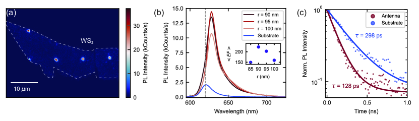
We then studied the PL dynamics in coupled and uncoupled monolayer by collecting time resolved luminescence traces of with a streak camera setup (see Methods). As depicted in Figure 2c, we observe a two-fold reduction of the decay lifetime for monolayers coupled to the nanoantenna near field, showing lifetimes of ps, compared to ps on bare substrate. Note, PL lifetimes in TMDCs are mainly limited by non-radiative processes, even at low power densities [7], hindering the extraction of an effective value of the spontaneous rate enhancement. In our experiments, we employed a pump fluence of 120 J/cm2 to obtain appreciable signal to noise ratio, too large to neglect the impact of non-radiative processes in time resolved experiments [11]. To elucidate the role of strain in the PL experiments, we prepared a control sample, where a WS2 monolayer is transferred on top of SiO2 nanopillars with the same geometry and dimensions of the GaP nanoantennas. The nanopillar provides a deformation centre, where strain is introduced in the monolayer, while lacking optical Mie resonances owing to its lower refractive index [27]. The experimental analysis of the control sample is presented in Supplementary Note IV. In strained WS2 we observe the presence of a strained exciton peak at the pillar sites, where a slight enhancement of the PL intensity could be detected. However, we observe no changes in the PL lifetime when compared to unstrained monolayers (Supplementary Figure 5b). This effect is consistent with previous reports where strain does not significantly impact the luminescence lifetime of WS2 monolayers [37], we thus ascribe the reduction of PL lifetime in our hybrid 2Ds semiconductor-dielectric system to the Purcell effect.
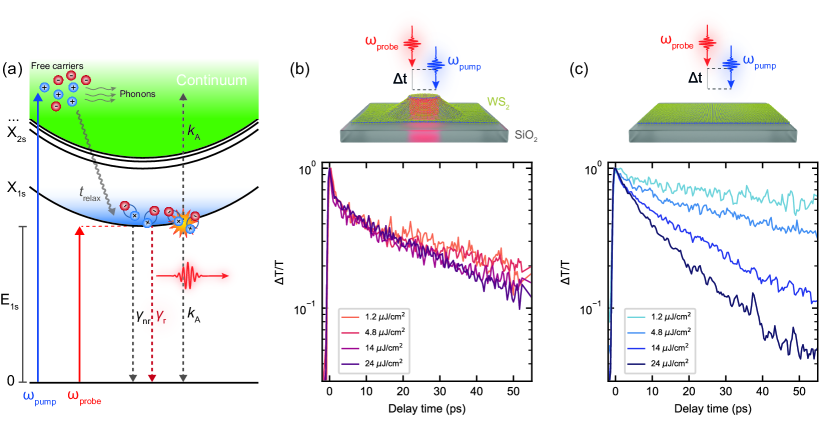
Ultrafast dynamics of coupled and uncoupled WS2 excitons To obtain additional insight on the exciton recombination dynamics in hybrid 2D semiconductor-dielectric nanoantennas, we investigated the coupled nanophotonic systems by means of non-degenerate ultrafast pump-probe spectroscopy (see Methods and Supplementary Note V). Figure 3a depicts a schematic of the excitons’ dynamics in a monolayer TMDC under non-resonant optical excitation. The absorption of high energy photons leads to the formation of free carriers in the high-lying bands, which undergo relaxation and formation of the exciton species via emission of phonons on a sub-100 fs timescale [38]. Due to the Wannier-Mott character, excitons diffuse in the crystal and the overall dynamics are described as the product of the spontaneous emission rate () and the non-radiative recombination rate (), e.g. from phonon, defects or carrier scattering, and EEA. The exciton population dynamics are described by the following equation:
| (2) |
where is the generation rate of excitons, is the diffusion coefficient and is the EEA coefficient. When the exciton population density () is small, the recombination dynamics are dominated by the sum of radiative and non-radiative processes. As increases, the quadratic term of the EEA starts to dominate the dynamics, leading to a fast decay of the photogenerated excitons [11]. Diffusion related effects are be expected to take place on a fast timescale, owing to exciton in-plane diffusion coefficients in the order of 200 nm2/ps [13], and further increased by the effect of strain-induced exciton funnelling [39].
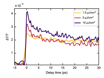
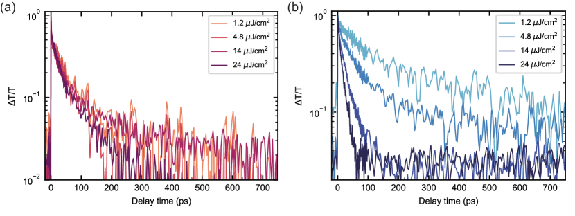
We compare the dynamics for excitons coupled with a resonant nanoantenna to that of a monolayer on bare SiO2 substrate. By resonantly probing the 1s-exciton state, we investigate the impact of EEA processes in the exciton recombination dynamics as a function of the pump fluence, directly proportional to the photoexcited exciton population. Figure 3b shows the transient absorption dynamics for a WS2 monolayer deposited on a resonant GaP nanoantenna (radius 90 nm, height 100 nm), as a function of the pump beam fluence. We observe that the pump has negligible effects on the exciton lifetime, exhibiting minor changes for the range of fluences employed in our experiments, at the same time presenting a fast recombination process at zero-time delay, in the order of 1 ps, independent on the excitation fluence. Remarkably, we observe the absence of the onset of EEA processes, as expected for uncoupled excitons under fluences above 10 J/cm2 [11], further confirmed in WS2 deposited on the other resonant nanoantennas (see Supplementary Note VI). Note, that while the strain values extracted from the exciton redshift changes between nanoantennas, in the range 0.15 - 0.45 %, the dynamics of coupled excitons are not significantly affected. These dynamics found for coupled excitons are in striking contrast with those observed in uncoupled monolayers. As shown in Figure 3c, in the transient absorption signal of a monolayer WS2 on SiO2 substrate we observe clear changes in the exciton dynamics as a function of the pump fluence, in the form of the onset of a bimolecular recombination process, as expected from the role of EEA dominating the dynamics even under fluences as small as 10 J/cm2 [11]. As EEA processes can be neglected at the lowest fluence, the observed reduction of the lifetime in coupled excitons can be interpreted as the main effect of the Purcell effect, increasing the radiative recombination rate and reducing the overall exciton lifetime. In Supplementary Note VII, we compare the exciton dynamics at longer timescales, where the population of uncoupled excitons decays in 100 ps for excitation above 10 J/cm2.
We demonstrate the role of optical Mie resonances on WS2 excitons’ dynamics in Supplementary Note VIII, where we transferred WS2 monolayers on top of non-resonant GaP nanoantennas. As the Mie resonances are spectrally decoupled to the WS2 exciton (Supplementary Figure 10d), we observe negligible PL enhancement and the presence of an EEA onset in the ultrafast dynamics, as observed for monolayers on SiO2 substrates. Moreover, as the off-resonant antenna provides a larger contact area between GaP and WS2, compared to smaller resonant antennas, we conclude that the dielectric permittivity of the surrounding material does not impact the exciton dynamics within the investigated size ranges [40].
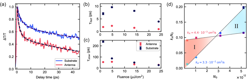
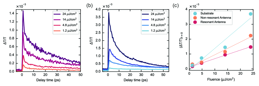
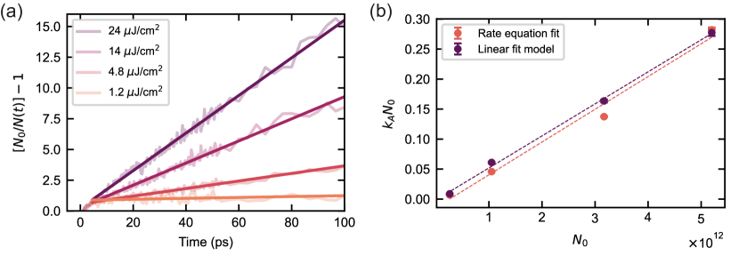
Radiative suppression of exciton-exciton annihilation via enhanced light-matter coupling The ultrafast optical response of 2D semiconductors is described by the interplay of different effects determining their dynamics [41]. For instance, band gap renormalization and changes in the binding energy, resulting in spectral shifts of the exciton resonance, or broadening of the exciton linewidth, via scattering and collisions, competing with Pauli blocking of photoexcited carriers. However, for excitation energies above the WS2 bandgap, as in our experiments, the ultrafast response is dominated by Pauli blocking [42]. Furthermore, large exciton binding energies hinder auto-ionization of resonantly excited excitons in high-lying states, and we exclude thermal effects in our experiments following a linear dependence of the differential transmission signal modulation at zero time delay as a function of the pump power (see Supplementary Note IX). In our experiments, the dynamics are thus described within the picture of a thermalized population of the WS2 1s-exciton state. We fit the ultrafast exciton dynamics with a biexponential model (Figure 4a) and extract the values of the fast and slow lifetime components, as shown in Figure 4b. For all the coupled monolayers, we observe the presence of a fast sub-ps decay of the exciton population, independent on the pump fluence, and limited by the temporal resolution of our setup. As shown in Supplementary Figure 6, we compare the ultrafast dynamics of strained excitons to that of flat excitons on SiO2 substrate, where no sub-ps dynamics are observed in strained WS2. This fast component is related to the formation process of excitons under above bandgap excitation [43, 44] and proportional to the exciton population generated in the semiconducting layer, where excitons rapidly reach the thermalized state [45, 46]. As the fast dynamic is observed only for coupled excitons (see Supplementary Note VI), we ascribe this effect to the enhanced absorption rate via near field coupling with the optical Mie resonances, leading to higher exciton densities. We extract the near field induced absorption enhancement as the ratio of the slow lifetime components on the antenna () and on the substrate (). At fluences of 1.2 and 4.8 J/cm2, we extract a constant value of , while under higher fluences above 10 J/cm2, the ratio is reduced by the impact of EEA processes. As is proportional to the near field intensity, [35], the extracted value is consistent with the expected near field enhancement, as shown in Figure 1d. At low fluences, the effect of EEA and non-radiative processes can be neglected, allowing the extraction of a lower bound value of the enhancement of the spontaneous emission rate for coupled excitons. By comparing the slow lifetime components ratio at low power, we extract a Purcell factor of . Finally, we extract the EEA coefficient, , by fitting the data with a rate equation model (see Supplementary Note X for details on the model and fitting procedure) and plot the values as a function of the exciton density in Figure 4d. From the slope of the linear fit, we extract a value of cm2/s in the case of coupled WS2 monolayer. Instead, for uncoupled monolayer on a glass substrate we found cm2/s, one order of magnitude higher than for the nanoantenna coupled WS2 and consistent with previous reports [12].
Comparing the number of scattering events () to the injected exciton density (), we observed two regimes determined by the EEA processes, denoted as Region I and II in Figure 4d. In Region I, at lower exciton densities, coupled excitons exhibit a higher number of scattering events compared to the uncoupled case. This is a direct consequence of the enhanced absorption rate, resulting in a larger at the antenna position, directly inducing the fast picosecond recombination observed in our experiments. However, above a certain density threshold, highlighted as Region II in Figure 4d, we observe that values for uncoupled excitons overtake the value for coupled ones, which, on the contrary, exhibit only a slight increase. Here, the exciton recombination is dominated by the radiative decay rate, as more excitons are depleted faster via the enhanced radiative channel. The lower EEA coefficient in coupled excitons is a direct consequence of the quadratic dependence of to the excitonic population shown in Equation 2. The probability for excitons to diffuse and participate in scattering processes is hindered by the fast radiative recombination, reducing the overall number of non-radiative EEA events, directly increasing the quantum efficiency and realizing higher exciton densities in coupled WS2 monolayers.
Discussion
In summary, we demonstrated the suppression of EEA processes in a hybrid 2D semiconductor-dielectric system by coupling excitons in monolayer WS2 with optical Mie resonances of GaP dielectric nanoantennas. The system reaches an intermediate light-matter coupling regime with PL enhancement factors above 102, as a result of enhanced absorption and spontaneous emission rates. From the ultrafast exciton dynamics, we show the resilience of nanoantenna coupled excitons to sustain higher pump fluences without the onset of EEA processes. We extract one order of magnitude smaller EEA coefficients, together with absorption enhancement of 3.9 and Purcell factor of 4.5. Owing to the increased radiative recombination rate, the exciton population is depleted faster via photon emission, suppressing the onset of EEA observed in uncoupled TMDCs monolayers. Engineering the photonic environment represents a novel opportunity to further reduce EEA processes in 2D semiconductors, for instance via integration with van der Waals metasurfaces [47]. Moreover, rationally designed hybrid nanophotonic systems based on 2D materials offer a vast toolbox for shaping and controlling light field at the nanoscale, for realizing higher spontaneous emission rates. Suppression of EEA via integration of 2D semiconductors with hybrid architectures can be extended to van der Waals heterostructures and Moiré systems, merging nanophotonic with many body physics and strongly correlated exciton phases [48], and to novel hybrid platforms based on 2D and bulk van der Waals materials, as building blocks of optically resonant nanostructures [49, 50].
Methods
Sample fabrication GaP nanoantennas are fabricated with a top-down process using a combination of electron beam lithography (EBL) and reactive ion etching (RIE). 100 nm GaP and 80 nm SiO2 are grown on a glass substrate by sputtering. A double layer of Polymethylmethacrylate (PMMA) resist and an additional conducting layer, to avoid charging effects, are spin coated on the sample. The resist is patterned with an EBL system, at 30 kV acceleration voltage, 20 m aperture, dose of 330 C/cm2, and then developed in a 1:3 solution of Methylisobutylketone (MIBK) and isopropanol. 3 nm Ti and 30 nm Au are evaporated with an electron beam evaporator, acting as etching mask. We first removed the SiO2 layer via RIE and etch the gold with a standard gold etchant. The SiO2 left on the sample is used as a mask for the GaP RIE step, and is finally removed with an additional RIE etching, resulting in the desired GaP nanostructures on fused silica substrate. Monolayers of WS2 are exfoliated from a commercial single crystal (HQ Graphene) and deposited on top of the nanoantennas with an all-dry transfer technique based on polydimethylsiloxane (PDMS) [51] in a home build transfer setup.
Numerical simulations FDTD simulations were carried out with a commercial software (Ansys Lumerical). The refractive index of the amorphous GaP film are extracted from ellipsometry measurements [52].
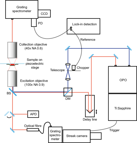
Optical spectroscopy Dark field scattering experiments are performed in a commercial WiTec system with a broadband white light source. For PL and ultrafast spectroscopy experiments, we show a detailed schematics of the experimental setup in Supplementary Note V. The sample is mounted on a piezoelectric stage coupled to an inverted microscope system for mapping and fine tuning of its position. As excitation, we employ the frequency doubled output of a 180 femtoseconds pulsed tunable Ti:sapphire laser (Coherent Chameleon Ultra II) with repetition rate of 80 MHz. The PL signal is collected with a monochromator and CCD detector (Princeton Instruments) or an avalanche photodetector (MDP) for PL mapping. The time resolved PL is acquired by directing the light to a monochromator and streak camera system (Hamamatsu). For pump-probe experiments, the frequency doubled Ti:sapphire laser is modulated at a frequency of 1990 Hz, with a mechanical chopper, and is used as the pump beam. The same laser drives a tunable optical parametric oscillator, which frequency doubled signal output is sent to an optical delay line and used as the probe. We excite the 2D semiconductor with laser pulses at 435 nm (2.85 eV), while resonantly probing the 1s-exciton transition of WS2 monolayers at approximately 620 nm (2 eV), tuned to the maximum modulation of the WS2 response for each sample. The ultrafast dynamics are then recorded with a photodiode at the output of a grating monochromator, and with lock-in amplification. As the probe beam is resonantly exciting the exciton population, we carefully calibrated the impact of the probe energy by avoiding the presence of a fast decay peak in the response of the WS2. This is shown in Supplementary Note XI. We set the probe beam to a fluence of 1.5 J/cm2 for all our experiments.
Data availability
The data that support the findings of this study are available from the corresponding author upon reasonable request.
References
- Klingshirn [2012] C. F. Klingshirn, Semiconductor Optics, Graduate Texts in Physics (Springer Berlin Heidelberg, Berlin, Heidelberg, 2012).
- Efros and Nesbitt [2016] A. L. Efros and D. J. Nesbitt, Origin and control of blinking in quantum dots, Nature Nanotechnology 11, 661 (2016).
- Shen et al. [2007] Y. C. Shen, G. O. Mueller, S. Watanabe, N. F. Gardner, A. Munkholm, and M. R. Krames, Auger recombination in InGaN measured by photoluminescence, Applied Physics Letters 91, 141101 (2007).
- Wang et al. [2004] F. Wang, G. Dukovic, E. Knoesel, L. E. Brus, and T. F. Heinz, Observation of rapid Auger recombination in optically excited semiconducting carbon nanotubes, Physical Review B 70, 241403 (2004).
- Yu et al. [2016] Y. Yu, Y. Yu, C. Xu, A. Barrette, K. Gundogdu, and L. Cao, Fundamental limits of exciton-exciton annihilation for light emission in transition metal dichalcogenide monolayers, Physical Review B 93, 201111 (2016).
- Mak and Shan [2016] K. F. Mak and J. Shan, Photonics and optoelectronics of 2D semiconductor transition metal dichalcogenides, Nature Photonics 10, 216 (2016).
- Wang et al. [2018] G. Wang, A. Chernikov, M. M. Glazov, T. F. Heinz, X. Marie, T. Amand, and B. Urbaszek, Colloquium: Excitons in atomically thin transition metal dichalcogenides, Reviews of Modern Physics 90, 021001 (2018).
- Rodin et al. [2020] A. Rodin, M. Trushin, A. Carvalho, and A. H. Castro Neto, Collective excitations in 2D materials, Nature Reviews Physics 2, 524 (2020).
- Turunen et al. [2022] M. Turunen, M. Brotons-Gisbert, Y. Dai, Y. Wang, E. Scerri, C. Bonato, K. D. Jöns, Z. Sun, and B. D. Gerardot, Quantum photonics with layered 2D materials, Nature Reviews Physics 4, 219 (2022).
- Kumar et al. [2014] N. Kumar, Q. Cui, F. Ceballos, D. He, Y. Wang, and H. Zhao, Exciton-exciton annihilation in MoSe2 monolayers, Physical Review B 89, 125427 (2014).
- Sun et al. [2014] D. Sun, Y. Rao, G. A. Reider, G. Chen, Y. You, L. Brézin, A. R. Harutyunyan, and T. F. Heinz, Observation of Rapid Exciton–Exciton Annihilation in Monolayer Molybdenum Disulfide, Nano Letters 14, 5625 (2014).
- Yuan and Huang [2015] L. Yuan and L. Huang, Exciton dynamics and annihilation in WS2 2D semiconductors, Nanoscale 7, 7402 (2015).
- Mouri et al. [2014] S. Mouri, Y. Miyauchi, M. Toh, W. Zhao, G. Eda, and K. Matsuda, Nonlinear photoluminescence in atomically thin layered WSe2 arising from diffusion-assisted exciton-exciton annihilation, Physical Review B 90, 155449 (2014).
- Masubuchi et al. [2017] S. Masubuchi, M. Okada, R. Moriya, T. Taniguchi, R. Kitaura, T. Kuroda, T. Machida, K. Watanabe, and Y. Hoshi, Suppression of exciton-exciton annihilation in tungsten disulfide monolayers encapsulated by hexagonal boron nitrides, Physical Review B 95, 1 (2017).
- Lien et al. [2019] D. H. Lien, S. Z. Uddin, M. Yeh, M. Amani, H. Kim, J. W. Ager, E. Yablonovitch, and A. Javey, Electrical suppression of all nonradiative recombination pathways in monolayer semiconductors, Science 364, 468 (2019).
- Kim et al. [2021] H. Kim, S. Z. Uddin, N. Higashitarumizu, E. Rabani, and A. Javey, Inhibited nonradiative decay at all exciton densities in monolayer semiconductors, Science 373, 448 (2021).
- Han et al. [2018] B. Han, C. Robert, E. Courtade, M. Manca, S. Shree, T. Amand, P. Renucci, T. Taniguchi, K. Watanabe, X. Marie, L. E. Golub, M. M. Glazov, and B. Urbaszek, Exciton States in Monolayer MoSe2 and MoTe2 Probed by Upconversion Spectroscopy, Physical Review X 8, 031073 (2018).
- Binder et al. [2019] J. Binder, J. Howarth, F. Withers, M. R. Molas, T. Taniguchi, K. Watanabe, C. Faugeras, A. Wysmolek, M. Danovich, V. I. Fal’ko, A. K. Geim, K. S. Novoselov, M. Potemski, and A. Kozikov, Upconverted electroluminescence via Auger scattering of interlayer excitons in van der Waals heterostructures, Nature Communications 10, 2335 (2019).
- Linardy et al. [2020] E. Linardy, D. Yadav, D. Vella, I. A. Verzhbitskiy, K. Watanabe, T. Taniguchi, F. Pauly, M. Trushin, and G. Eda, Harnessing Exciton-Exciton Annihilation in Two-Dimensional Semiconductors, Nano Letters 20, 1647 (2020).
- Lin et al. [2021] K.-Q. Lin, C. S. Ong, S. Bange, P. E. Faria Junior, B. Peng, J. D. Ziegler, J. Zipfel, C. Bäuml, N. Paradiso, K. Watanabe, T. Taniguchi, C. Strunk, B. Monserrat, J. Fabian, A. Chernikov, D. Y. Qiu, S. G. Louie, and J. M. Lupton, Narrow-band high-lying excitons with negative-mass electrons in monolayer WSe2, Nature Communications 12, 1 (2021).
- Sortino et al. [2019] L. Sortino, P. G. Zotev, S. Mignuzzi, J. Cambiasso, D. Schmidt, A. Genco, M. Aßmann, M. Bayer, S. A. Maier, R. Sapienza, and A. I. Tartakovskii, Enhanced light-matter interaction in an atomically thin semiconductor coupled with dielectric nano-antennas, Nature Communications 10, 5119 (2019).
- Yuan et al. [2021] L. Yuan, J. Jeong, K. W. Chi Kwock, E. S. Yanev, M. Grandel, D. A. Rhodes, T. S. Luk, P. J. Schuck, D. Yarotski, J. C. Hone, I. Brener, and R. P. Prasankumar, Manipulation of Exciton Dynamics in Single-Layer WSe2 Using a Toroidal Dielectric Metasurface, Nano Letters 21, 9930 (2021).
- Fang et al. [2022] J. Fang, K. Yao, T. Zhang, M. Wang, T. Jiang, S. Huang, B. A. Korgel, M. Terrones, A. Alù, and Y. Zheng, Room‐Temperature Observation of Near‐Intrinsic Exciton Linewidth in Monolayer WS2, Advanced Materials 34, 2108721 (2022).
- Zotev et al. [2022] P. G. Zotev, Y. Wang, L. Sortino, T. Severs Millard, N. Mullin, D. Conteduca, M. Shagar, A. Genco, J. K. Hobbs, T. F. Krauss, and A. I. Tartakovskii, Transition Metal Dichalcogenide Dimer Nanoantennas for Tailored Light–Matter Interactions, ACS Nano 16, 6493 (2022).
- Petrić et al. [2022] M. M. Petrić, M. Kremser, M. Barbone, A. Nolinder, A. Lyamkina, A. V. Stier, M. Kaniber, K. Müller, and J. J. Finley, Tuning the Optical Properties of a MoSe2 Monolayer Using Nanoscale Plasmonic Antennas, Nano Letters 22, 561 (2022).
- Luo et al. [2018] Y. Luo, G. D. Shepard, J. V. Ardelean, D. A. Rhodes, B. Kim, K. Barmak, J. C. Hone, and S. Strauf, Deterministic coupling of site-controlled quantum emitters in monolayer WSe2 to plasmonic nanocavities, Nature Nanotechnology 13, 1137 (2018).
- Sortino et al. [2021] L. Sortino, P. G. Zotev, C. L. Phillips, A. J. Brash, J. Cambiasso, E. Marensi, A. M. Fox, S. A. Maier, R. Sapienza, and A. I. Tartakovskii, Bright single photon emitters with enhanced quantum efficiency in a two-dimensional semiconductor coupled with dielectric nano-antennas, Nature Communications 12, 6063 (2021).
- Kuznetsov et al. [2016] A. I. Kuznetsov, A. E. Miroshnichenko, M. L. Brongersma, Y. S. Kivshar, and B. Luk’yanchuk, Optically resonant dielectric nanostructures, Science 354, 846 (2016).
- Staude et al. [2013] I. Staude, A. E. Miroshnichenko, M. Decker, N. T. Fofang, S. Liu, E. Gonzales, J. Dominguez, T. S. Luk, D. N. Neshev, I. Brener, and Y. Kivshar, Tailoring directional scattering through magnetic and electric resonances in subwavelength silicon nanodisks, ACS Nano 7, 7824 (2013).
- Miroshnichenko et al. [2015] A. E. Miroshnichenko, A. B. Evlyukhin, Y. F. Yu, R. M. Bakker, A. Chipouline, A. I. Kuznetsov, B. Luk’yanchuk, B. N. Chichkov, and Y. S. Kivshar, Nonradiating anapole modes in dielectric nanoparticles, Nature Communications 6, 8069 (2015).
- Cortés et al. [2022] E. Cortés, F. J. Wendisch, L. Sortino, A. Mancini, S. Ezendam, S. Saris, L. de S. Menezes, A. Tittl, H. Ren, and S. A. Maier, Optical Metasurfaces for Energy Conversion, Chemical Reviews 122, 15082 (2022).
- Cambiasso et al. [2017] J. Cambiasso, G. Grinblat, Y. Li, A. Rakovich, E. Cortés, and S. A. Maier, Bridging the Gap between Dielectric Nanophotonics and the Visible Regime with Effectively Lossless Gallium Phosphide Antennas, Nano Letters 17, 1219 (2017).
- Uddin et al. [2021] S. Z. Uddin, E. Rabani, and A. Javey, Universal Inverse Scaling of Exciton–Exciton Annihilation Coefficient with Exciton Lifetime, Nano Letters 21, 424 (2021).
- Pelton et al. [2019] M. Pelton, S. D. Storm, and H. Leng, Strong coupling of emitters to single plasmonic nanoparticles: exciton-induced transparency and Rabi splitting, Nanoscale 11, 14540 (2019).
- Koenderink [2017] A. F. Koenderink, Single-Photon Nanoantennas, ACS Photonics 4, 710 (2017).
- Sortino et al. [2020] L. Sortino, M. Brooks, P. G. Zotev, A. Genco, J. Cambiasso, S. Mignuzzi, S. A. Maier, G. Burkard, R. Sapienza, and A. I. Tartakovskii, Dielectric Nanoantennas for Strain Engineering in Atomically Thin Two-Dimensional Semiconductors, ACS Photonics 7, 2413 (2020).
- Niehues et al. [2018] I. Niehues, R. Schmidt, M. Drüppel, P. Marauhn, D. Christiansen, M. Selig, G. Berghäuser, D. Wigger, R. Schneider, L. Braasch, R. Koch, A. Castellanos-Gomez, T. Kuhn, A. Knorr, E. Malic, M. Rohlfing, S. Michaelis de Vasconcellos, and R. Bratschitsch, Strain Control of Exciton-Phonon Coupling in Atomically Thin Semiconductors, Nano Letters 18, 1751 (2018).
- Trovatello et al. [2020] C. Trovatello, F. Katsch, N. J. Borys, M. Selig, K. Yao, R. Borrego-Varillas, F. Scotognella, I. Kriegel, A. Yan, A. Zettl, P. J. Schuck, A. Knorr, G. Cerullo, and S. D. Conte, The ultrafast onset of exciton formation in 2D semiconductors, Nature Communications 11, 5277 (2020).
- Rosati et al. [2021] R. Rosati, R. Schmidt, S. Brem, R. Perea-Causín, I. Niehues, J. Kern, J. A. Preuß, R. Schneider, S. Michaelis de Vasconcellos, R. Bratschitsch, and E. Malic, Dark exciton anti-funneling in atomically thin semiconductors, Nature Communications 12, 7221 (2021).
- Steinhoff et al. [2021] A. Steinhoff, F. Jahnke, and M. Florian, Microscopic theory of exciton-exciton annihilation in two-dimensional semiconductors, Physical Review B 104, 1 (2021).
- Dal Conte et al. [2020] S. Dal Conte, C. Trovatello, C. Gadermaier, and G. Cerullo, Ultrafast Photophysics of 2D Semiconductors and Related Heterostructures, Trends in Chemistry 2, 28 (2020).
- Trovatello et al. [2022] C. Trovatello, F. Katsch, Q. Li, X. Zhu, A. Knorr, G. Cerullo, and S. Dal Conte, Disentangling Many-Body Effects in the Coherent Optical Response of 2D Semiconductors, Nano Letters 22, 5322 (2022).
- Cunningham et al. [2016] P. D. Cunningham, K. M. McCreary, and B. T. Jonker, Auger Recombination in Chemical Vapor Deposition-Grown Monolayer WS2, The Journal of Physical Chemistry Letters 7, 5242 (2016).
- Ceballos and Zhao [2017] F. Ceballos and H. Zhao, Ultrafast Laser Spectroscopy of Two‐Dimensional Materials Beyond Graphene, Advanced Functional Materials 27, 1604509 (2017).
- Shah [1996] J. Shah, Ultrafast Spectroscopy of Semiconductors and Semiconductor Nanostructures, Springer Series in Solid-State Sciences, Vol. 115 (Springer, Berlin, Heidelberg, 1996).
- Estrada-Real et al. [2022] A. Estrada-Real, I. Paradisanos, P. R. Wiecha, J.-M. Poumirol, A. Cuche, G. Agez, D. Lagarde, X. Marie, V. Larrey, J. Müller, G. Larrieu, V. Paillard, and B. Urbaszek, Probing the optical near-field interaction of Mie nanoresonators with atomically thin semiconductors, (2022), arXiv:2210.14058 .
- Kühner et al. [2022] L. Kühner, L. Sortino, B. Tilmann, T. Weber, K. Watanabe, T. Taniguchi, S. A. Maier, and A. Tittl, High‐Q Nanophotonics Over the Full Visible Spectrum Enabled by Hexagonal Boron Nitride Metasurfaces, Advanced Materials, 35, 2209688 (2022) .
- Mak and Shan [2022] K. F. Mak and J. Shan, Semiconductor moiré materials, Nature Nanotechnology 17, 686 (2022).
- Lin et al. [2022] H. Lin, Z. Zhang, H. Zhang, K.-t. Lin, X. Wen, Y. Liang, Y. Fu, A. K. T. Lau, T. Ma, C.-w. Qiu, and B. Jia, Engineering van der Waals Materials for Advanced Metaphotonics, Chemical Reviews 122, 15204 (2022).
- Weber et al. [2022] T. Weber, L. Kühner, L. Sortino, A. B. Mhenni, N. P. Wilson, J. Kühne, J. J. Finley, S. A. Maier, and A. Tittl, Strong light-matter interaction with self-hybridized bound states in the continuum in monolithic van der Waals metasurfaces, (2022), arXiv:2209.01944 .
- Castellanos-Gomez et al. [2014] A. Castellanos-Gomez, M. Buscema, R. Molenaar, V. Singh, L. Janssen, H. S. J. van der Zant, and G. A. Steele, Deterministic transfer of two-dimensional materials by all-dry viscoelastic stamping, 2D Materials 1, 011002 (2014).
- Tilmann et al. [2020] B. Tilmann, G. Grinblat, R. Berté, M. Özcan, V. F. Kunzelmann, B. Nickel, I. D. Sharp, E. Cortés, S. A. Maier, and Y. Li, Nanostructured amorphous gallium phosphide on silica for nonlinear and ultrafast nanophotonics, Nanoscale Horizons 5, 1500 (2020).
- Alexeev et al. [2017] E. M. Alexeev, A. Catanzaro, O. V. Skrypka, P. K. Nayak, S. Ahn, S. Pak, J. Lee, J. I. Sohn, K. S. Novoselov, H. S. Shin, and A. I. Tartakovskii, Imaging of Interlayer Coupling in van der Waals Heterostructures Using a Bright-Field Optical Microscope, Nano Letters 17, 5342 (2017).
- Li et al. [2014] Y. Li, A. Chernikov, X. Zhang, A. Rigosi, H. M. Hill, A. M. van der Zande, D. A. Chenet, E.-M. Shih, J. Hone, and T. F. Heinz, Measurement of the optical dielectric function of monolayer transition-metal dichalcogenides: MoS2, MoSe2, WS2 and WSe2, Physical Review B 90, 205422 (2014).
Acknowledgements
S.A.M acknowledges the Lee Lucas chair in physics, funding by the EPSRC (EP/WO1707511) and the Australian Research Council (Centre of Excellence in Future Low-Energy Electronics Technologies - CE 170100039). L.S. further acknowledges funding support through a Humboldt Research Fellowship from the Alexander von Humboldt Foundation. Our studies were partially supported by the Center for NanoScience (CeNS) - Faculty of Physics, Ludwig-Maximilians University Munich.
Conflict of interest
The authors declare no competing interests.
Supplementary information for: Radiative suppression of exciton-exciton annihilation in a two-dimensional semiconductor
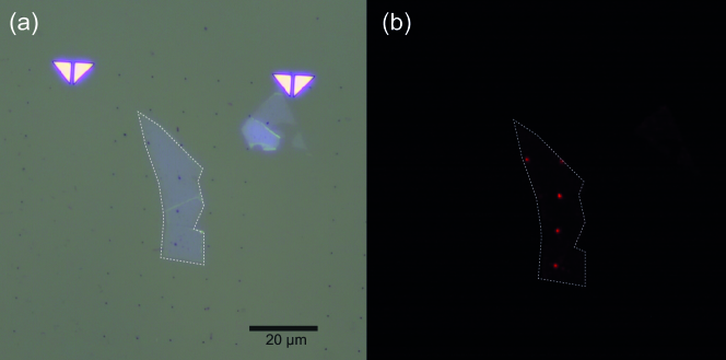
Supplementary note I: Bright field and PL imaging of the hybrid 2D semiconductor-dielectric nanoantenna sample
Supplementary note II: Dark field scattering of hybrid 2D semiconductor-dielectric nanoantennas
Supplementary note III: Photoluminescence enhancement factor
The PL enhancement factor, , is extracted from experiments as [21]:
| (3) |
where, is the integrated PL intensity for WS2 coupled to the nano-antennas, that of the uncoupled WS2 on planar substrate. These are normalized on the PL excitation area, , defined by the excitation laser spot size, and the geometrical cross section of the cylindrical nanoantenna, .
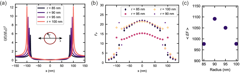
We calculated the upper bound of the from finite-difference time-domain (FDTD) numerical simulations, following:
| (4) |
where is the near field intensity, the Purcell factor, and the directivity enhancement of the nanoantenna coupled dipole. These values are normalized over the ones obtained for the uncoupled case of a dipole on silica substrate. We placed the dipole 0.5 nm above the edge of the nanoantenna, in order to maximize the values of field enhancement and [21]. Supplementary Figure 3a shows the near field values at the surface of the nanoantennas, taken at the top surface along the x-axis, as shown in the figure inset. Supplementary Figure 3b shows the values of the Purcell factor along the same x-axis, for an in-plane dipole emitting at 620 nm along the x-axis, placed 0.5 nm above the nanoantenna’s surface. For directivity simulations, we calculated the power emitted by the dipole source in the far field, integrated over the solid angle defined by the objective numerical aperture. We found values of for nanoantennas of radius of 100 nm, increasing with the antenna radius up to a value of for nanoantennas with radius of 85 nm. The product of these three ratios gives the upper bound of the , shown in Supplementary Figure 3c.
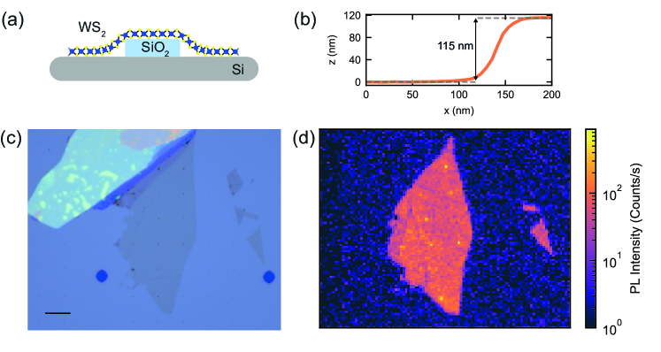
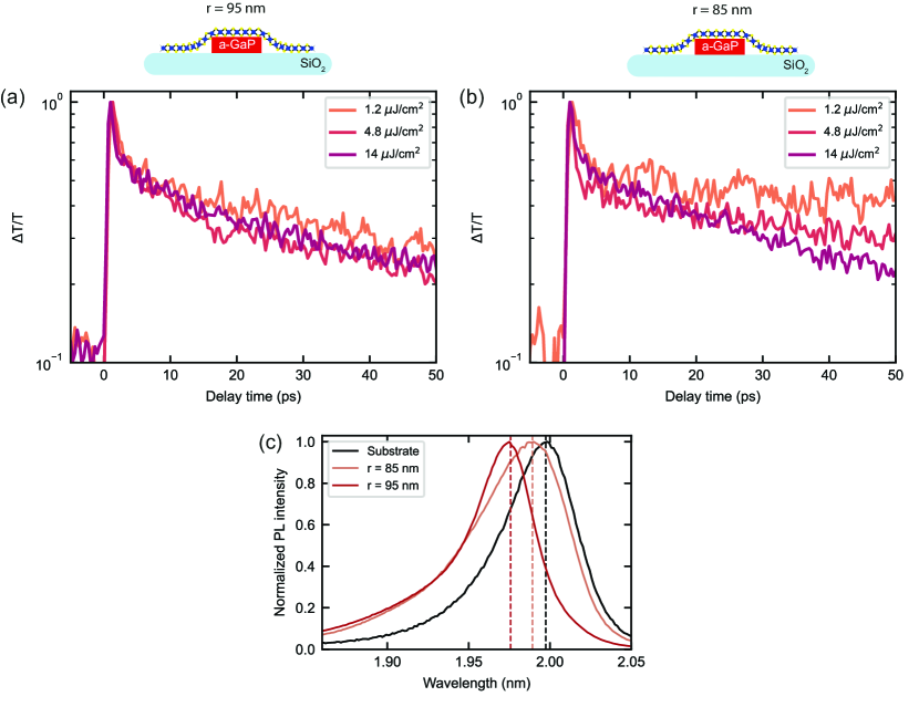
Supplementary note IV: Strained WS2 on SiO2 nanopillars
We fabricated silica nanopillars to eluidate the role of strain in the PL and dynamics in strained WS2 monolayers.
Supplementary Figure 4a shows the schematic of the sample. The SiO2 nanopillars are fabricated as follows. We employed a commercial Si wafer with a thermal SiO2 layer of nominal thickness of 300 nm. We used a first etching step for thinning the oxide layer down to 100 nm, the target height of the nanopillars. We then use a combination of electron beam lithography and reactive ion etching (RIE) to pattern the silica nanopillars. Supplementary Figure 4b shows an atomic force microscopy (AFM) profile of a fabricated nanopillar, revealing a height of 115 nm. The WS2 monolayer is exfoliated and transferred on the nanopillars with an all-dry PDMS based transfer technique. Supplementary Figure 4c shows the bright field image of the final sample. In Supplementary Figure 4d is shown the PL map of WS2 excited with a 180 femtosecond laser at 532 nm and average power of 6.5 nW. We observe a small increase of the integrated PL intensity when the monolayer is on top of the nanopillars.
Supplementary Figure 5a shows a representative PL spectrum collected on top of a single nanopillar, excited with a 532 nm laser pulse with average power of 1.4 W. At low power densities, we observe the presence of a broad excitonic peak red shifted from the exciton energy of the unstrained WS2 on the substrate (in gray), related to the effect of tensile strain on the exciton energy [36]. We probed the PL dynamics and observed negligible differences in the PL lifetimes (see Supplementary Figure 5b), as previously observed in strained WS2 [37]. From the fit of the PL spectra of different nanopillars, we extract the energy shift of the strained exciton resonance and calculate the relative tensile strain value. This is shown in Supplementary Figure 5c, where we extract values between 0.4% and 1.1%. Note, these are larger values than the ones observed in our hybrid 2D semiconductor-GaP nanoantenna sample.
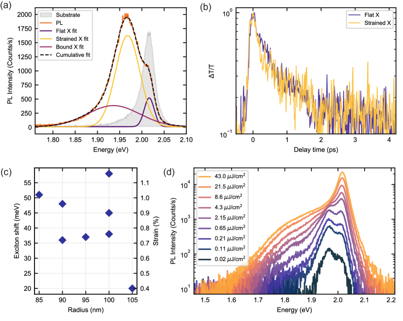
Supplementary Figure 5d shows the PL emission as a function of the excitation power for the same nanopillar shown in Supplementary Figure 5a. At low power densities, the strained exciton peak intensity is comparable or higher than the signal from the surrounding unstrained excitons. We ascribe this effect to funnelling, which pushes bright excitons towards the strained area [39]. Moreover, at higher power densities the unstrained exciton peak dominates the PL emission, together with the appearance of a broad peak at energies below 1.9 eV.
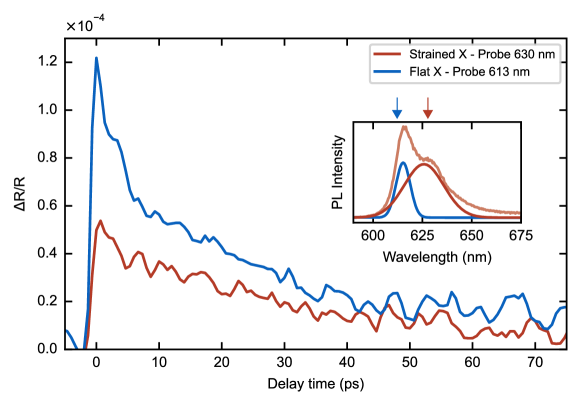
We further probed the ultrafast dynamics of flat and strained excitons. Supplementary Figure 6 shows the differential reflection () for the WS2 monolayer on top of a silica pillar with radius of 90 nm. We probed the exciton dynamics at two wavelengths, at 613 nm for the flat exciton and at 630 nm for the strained exciton (see PL in inset). The probe fluence was set at 1.2 W/cm2 and pump at 10.1 W/cm2. The high fluence conditions used to obtain a detectable signal in reflection measurements, are above the EEA onset. Indeed, for the flat exciton (blue curve) we observe a fast recombination dynamics related to EEA, while the strained exciton (red curve) we exhibit a slower recombination dynamics, with no fast component related to EEA. This exclude strain as the cause of the fast sub-ps dynamics observed when the WS2 monolayers are coupled to GaP nanoantennas, as discussed in the main text.
Supplementary note V: Experimental setup schematics
Supplementary note VI: Ultrafast dynamics of WS2 excitons coupled to additional resonant GaP nanoantennas
Supplementary note VII: Coupled and uncoupled exciton dynamics at long timescales
Supplementary note VIII: WS2 monolayer coupled to non-resonant GaP nanoantennas
We studied the effect of non-resonant GaP nanoantennas, with geometry of 50 nm height and radius of 320 nm, on the WS2 PL and dynamics.
Supplementary Figure 10a shows the bright field image of a transferred WS2 monolayer on arrays of non-resonant GaP nanoantennas. As shown in Supplementary Figure 10b, we observe negligible PL enhancement when the monolayer is transferred on top of such nanoantenna, and a small redshift in the exciton peak corresponding to 0.05% strain. Supplementary Figure 10c shows the PL dynamics, where a small increase of lifetimes at longer timescales is observed for monolayers on GaP. Supplementary Figure 10d shows the dark field scattering of the studied sample, confirming the lack of spectral coupling between excitons and the optical resonances of the GaP nanoantenna, located at longer wavelengths above 700 nm. In Supplementary Figure 10e we report the exciton dynamics probed with the same experimental conditions as described in the main text. The effect of EEA is clearly observed in the dependence with the pump beam fluence. From the ultrafast dynamics, we extract a rate of cm2/s, consistent with the values observed for unstrained WS2 on silica substrates [12].
Supplementary note IX: Linear dependence of at zero time delay
Supplementary note X: Fitting procedure to extract EEA rates
To extract the EEA coefficient () from the experimental data, we implemented two procedures [11, 10]. The first procedure is done by fitting the data with the following equation:
| (5) |
This is a simplified case for Equation 2 in the main text. Here, we neglect the diffusion term and, as EEA processes are significant only at the early times, long recombination dynamics do not impact the extracted values of [10].
The second procedure consists in normalizing the zero-time delay modulation of the transient absorption, , by the value of , calculated for an absorption of 0.1% by WS2 monolayer at the pump wavelength [54]. As shown in Supplementary Figure 12a, the data are then fitted with the following equation:
| (6) |
From the slope of the linear fit, we extract the values of , at different excitation powers. As it is proportional to , we plot the obtained values as shown in Supplementary Figure 12b. From the slope of the linear fit we then extract the value of , which we found is not significantly affected by the chosen procedure.
Supplementary note XI: Effect of resonant probe pulse fluence on exciton dynamics