Effect of Environmental Screening and Strain on Optoelectronic Properties of Two-Dimensional Quantum Defects
Abstract
Point defects in hexagonal boron nitride (hBN) are promising candidates as single-photon emitters (SPEs) in nanophotonics and quantum information applications. The precise control of SPEs requires in-depth understanding of their optoelectronic properties. However, how the surrounding environment of host materials, including number of layers, substrates, and strain, influences SPEs has not been fully understood. In this work, we study the dielectric screening effect due to the number of layers and substrates, and the strain effect on the optical properties of carbon dimer and nitrogen vacancy defects in hBN from first-principles many-body perturbation theory. We report that the environmental screening causes lowering of the GW gap and exciton binding energy, leading to nearly constant optical excitation energy and exciton radiative lifetime. We explain the results with an analytical model starting from the BSE Hamiltonian with Wannier basis. We also show that optical properties of quantum defects are largely tunable by strain with highly anisotropic response, in good agreement with experimental measurements. Our work clarifies the effect of environmental screening and strain on optoelectronic properties of quantum defects in two-dimensional insulators, facilitating future applications of SPEs and spin qubits in low-dimensional systems.
I Introduction
Point defects in two-dimensional (2D) materials emerge to possess outstanding quantum properties such as stable single-photon emission, and have been exploited as spin quantum bits (qubits) for quantum information technologies [1, 2]. The single photon emitters (SPEs) in 2D materials are highly stable and tunable [2, 3, 4], and in particular, their optical activation can be spatially controlled and tuned by strain [5, 6], emphasizing the great potential of SPEs in 2D materials.
The defect candidates with promising quantum properties exhibit deep-level states or form defect-bound exciton. A large number of defects in hBN have been proposed since the report by Tran et al. [7]. So far, spin defect has been unambiguously identified from experiment [8, 9, 10, 11] and theory [12, 13]. Many of the other defects, whose atomic origins are yet to be determined, were found to be eV and eV SPEs [14, 15, 16, 17]. From theoretical predictions, [7, 14], boron dangling bonds [18], [19, 20], and carbon trimers [21, 22, 23, 24] were proposed to be defect candidates for the eV SPEs, while [25], [26], Stone-Wales defect [27], and carbon ring [28] were for the eV SPEs.
Among the proposed defect candidates, only partial experimental observations can be explained.
Most importantly, large variations of key physical properties including Zero-Phonon Line (ZPL), photoluminescence (PL) lifetime, and Huang-Rhys (HR) factor [29, 22] were observed. The physical origin of such variation is undetermined, with only some plausible explanations. For example, it is speculated that different substrates or sample thickness used in experiments may lead to variation [7, 15, 30]. Strain can be another source for the variation, as indicated by the past experimental studies [31, 14, 32]. Natural strain can be introduced when placing materials on top of substrates.
Theoretically, first-principles computation has been a powerful tool for identifying and proposing new defects as SPEs and spin qubits in 2D materials [33].
However, different structural models including monolayer,
multilayer or bulk hBN [13, 25, 21, 22, 23, 24] were used in different studies, which lead to difficulties of comparing with experiments and comparison among different theoretical studies. Furthermore, the effect of substrates has been mostly examined at the mean-field level by DFT with semilocal functionals, where excitonic effects are not considered [34, 35, 36].
At last, the effect of strain on optical properties such as absorption spectra, exciton binding energies, and radiative lifetime has not been investigated to our best knowledge.
In this work, from first-principles calculations, we investigate the environmental screening effect due to the layer thickness and substrates, as well as the strain effect on the optoelectronic properties of point defects in hBN. In order to pick representative defects for general conclusions, we choose as an example of extrinsic substitutional defects and as an example of native vacancy defects, both of which were commonly found in hBN and previously proposed to be possible eV and eV SPEs respectively.
Our results provide an estimation on how sensitive the excitation energy, exciton binding energy, and ZPL are to strain, and we explain their qualitative trends through molecular orbital theory.
We also provide intuitive and comprehensive understanding of environmental screening effect on defect properties through both first-principles many-body perturbation theory calculations and analytical models.
II Computational Method
The ground state calculations are carried out by density functional theory implemented in QuantumEspresso package[37], with the Perdew-Burke-Ernzerhof (PBE) exchange correlation functional [38]. We use the SG15 Optimized Norm-Conserving Vanderbilt (ONCV) pseudopotentials [39, 40] and 80 Ry wave function kinetic energy cutoff (320 Ry charge density cutoff) for plane wave basis set. The defect calculations are performed with supercell and k-point sampling, based on our convergence tests in previous studies [22, 31, 41].
We perform the many-body perturbation theory calculations with starting from PBE electronic states for the quasi-particle energies, and solve the Bethe-Salpeter equation (BSE) for the optical properties [42] with excitonic effects by the Yambo-code [43]. The GW calculation is carried out with 8 Ry response block size and 1800 energy bands for the dielectric matrix and self-energy, while we use 5 Ry and 80 bands for the BSE kernel and optical spectra calculations. With the 2D Coulomb truncation technique [44], the quasi-particle energies are converged within 10 meV at 33.5 a.u. vacuum size. More details on convergence tests can be found in SI Fig.S1 and Fig.S2.
We then calculate the ZPL by subtracting the Frank-Condon shift from the BSE excitation energy, where the is obtained by the constrained DFT (cDFT) technique [41]. By taking the excitation energy and exciton dipole moment from the solution of BSE, we then evaluate radiative lifetime for defects in 2D systems derived from the Fermi’s golden rule, with [45, 41, 41]. Here is the exciton energy, is the speed of light, is the modulus square of exciton dipole moment, and is reflective index, which is one for monolayer hBN.
For the study of layer thickness and substrate effects, we apply our recently-developed sum-up effective polarizability (-sum) with the reciprocal-space linear interpolation technique, in order to account for the impact of substrates and multilayers[46, 47]. This method allows us to separate the total interface into two subsystems as substrate pristine layers and defective monolayer, allowing a large saving of computational cost and avoiding artificial strain from enforcing lattice matching at interfaces.
III Results and Discussions
III.1 Electronic and Optical Properties of Defects in hBN
We start from the discussion of electronic structure and optical properties of defects in monolayer hBN at natural lattice constant, then followed by the discussion of strain and layer thickness/substrate effects.
We choose carbon dimer () and nitrogen vacancy () defects in hBN as our prototypical systems, both of which are common defects in hBN.
In particular was identified as a defect candidate for 4 eV SPE in hBN [48].
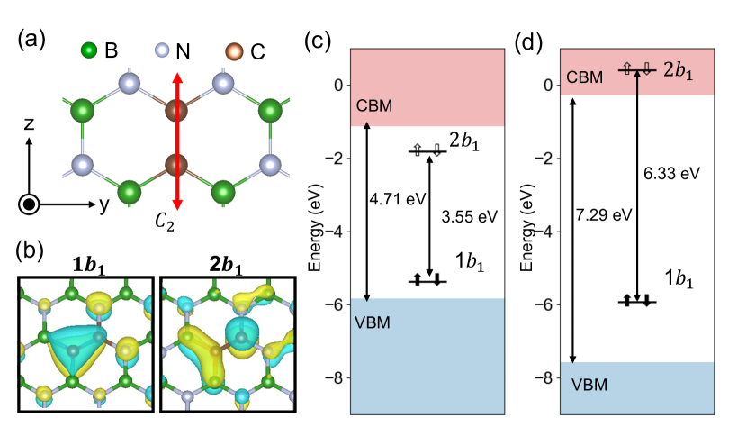
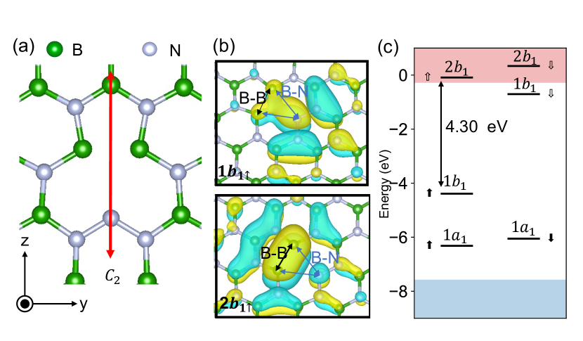
The atomic structures and electronic structures of and are shown in Fig. 1 and Fig. 2, respectively. The atomic structure shows that both and belong to the point symmetry group. We label the defect wave functions according to the irreducible representations to which they transform. In particular, the and states of , and and states of are of interest, as they correspond to the optically allowed intra-defect transitions [48, 49]. The comparison between the electronic structures at PBE and @PBE levels in Fig. 1c and d indicates that the quasiparticle correction shifts the occupied defect states downward and unoccupied states upward, opening up the defect gap of to 6.33 eV from 3.55 eV, and the defect gap of to 4.30 eV from 2.06 eV at PBE.
We then carried out BSE calculations for the related vertical excitation energy. The complete BSE spectra and the exciton wave function are presented in the SI Figs. S3 and S4. The results of indicate the presence of a single isolated peak related to the transition at the BSE excitation energy () of 4.44 eV, with a corresponding exciton binding energy of 1.89 eV and a radiative lifetime of 1.1 ns. The zero-phonon line energy () was calculated to be 4.32 eV by subtracting the Frack-Condon shift () of 0.12 eV from the BSE excitation energy. This result is in agreement with previous studies, where a ZPL around 4.3 eV has been obtained using cDFT with hybrid functional [48] or GW&BSE with a finite-size cluster approach [50]
We acknowledge the intricate nature of local structural distortion and optical transition of the defect, and the related detailed discussion is presented in the SI section III. However, to keep the main text concise, we focus on the transition at defect symmetry. The vertical transition energy for is 2.12 eV with a 57 ns radiative lifetime. The ZPL is 1.60 eV after subtracting the 0.52 eV from the vertical transition at BSE. Upon considering the transition to the lower symmetry ground state at symmetry due to out-of-plane distortion, the ZPL energy increases to 1.70 eV. Our result for transition related ZPL is lower than the previous calculation [51, 5] at hybrid functional, but consistent with previous BSE results at the same structure [52]. This highlights the important difference when excitonic effect is taken into account.
III.2 Effect of Strain
We investigate the effect of strain by applying it along two in-plane uniaxial directions, where the parallel () strain denotes the strain along the axis, and the perpendicular () strain denotes the direction perpendicular to the axis. The uniaxial strain here is defined as the stretching ratio of the lattice along a certain direction, with its magnitude as , where and are the lattice lengths before and after the strain is applied. denotes the macroscopic strain on the entire system. The strain tensor can thus be written as [6] where () is the angle between strain axis and () coordinate direction (as defined in Fig. 1(a) and Fig. 2(a)).
Due to the symmetry, the response of ZPL to the applied strain at the first order depends only on two in-plane diagonal components of the strain tensor, and thus can be written as:
| (1) |
where is the angle between the strain axis and axis. The energy response to strain is quantified by two linear strain susceptibilities . In order to understand the determining factors on ZPL energy change () when applying strain, can be decomposed into different contributions as follows.
| (2) |
where is the change of DFT single particle energy at the PBE level due to strain; is the change of quasipartical energy correction; is the change of exciton binding energy by solving BSE, and is the change of excited state relaxation energy (Frack-Condon shift) under strain.
We thus can separate ZPL’s strain susceptibility () into terms corresponding to different levels of contribution from Eq. 2,
| (3) |
By providing all the strain susceptibility components in Eq. 3, we can reveal the origin of ZPL response to strain.
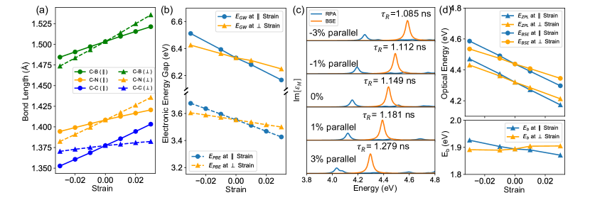
The effect of strain on the structural, electronic, and optical properties of in monolayer hBN is described in Fig. 3. Fig. 3(a) displays the change in three bond lengths, including the defect-defect bond length (C-C) and the defect-nearest-neighbor bond lengths (C-N and C-B). All three bond lengths increase linearly with strain (where a positive sign denotes stretching strain and a negative sign denotes compressing strain). Fig. 3(b) illustrates the change in defect electronic energy gap at PBE level () and G0W0@PBE level (). Fig. 3(c) and (d) present the optical properties of the defect emitter, including the absorption peak related to transition at RPA and BSE levels (c), and the corresponding BSE excitation energy (), ZPL (), and exciton binding energy () as a function of strain (d). Both the optical and electronic energy gaps of the defect-related transition exhibit a linear red shift with increasing strain, with the parallel strain resulting in a larger response compared to the perpendicular strain. However, the radiative lifetime () and exciton binding energy () show negligible response to the strain.
| 0.613 | 0.301 | 0.411 | -41.58 | -15.70 | -8.90 | 1.30 | -49.63 | |
| 0.144 | 0.629 | 0.688 | -17.75 | -11.40 | 2.82 | 4.64 | -36.49 | |
| - | ||||||||
| 0.463 | 1.664 | - | -59.70 | -19.32 | -14.27 | 40.35 | -105.20 | |
| 2.072 | 0.490 | - | 44.96 | 1.00 | 2.05 | 6.31 | 38.02 | |
The linearity of response to strain in Fig. 3 suggests that the linear response model represented by Eq. 1 and Eq. 3 is adequate. As a result, the strain susceptibility and bond length change rate (; related to the local bond length change speed under strain, will be defined later) are summarized in TABLE 1. Similar calculations were performed for the defect system, summarized in the same table as well.
The results of ZPL strain susceptibility () reveal that the defect exhibits a similar negative strain susceptibility (red shift of ZPL) in both and components, i.e. meV/% and meV/%. On the other hand, the defect exhibits a disparate strain response behavior in two directions, where the component of strain susceptibility is negative ( meV/%) and the component is positive ( meV/%). The sign difference on strain susceptibility reflects the different bonding nature of defects as discussed later. By substituting the two components of strain susceptibilities into Eq. 1, one can determine the ZPL energy shift under any uniaxial strain in the linear response regime. Previous experimental work has shown that the uniaxial strain susceptibility of 2 eV SPE ranges from -120 meV/% to 60 meV/% without specifying the strain direction [6, 53, 54]. Therefore, our calculated strain response for the defect falls within the experimental strain susceptibility range [55](more related discussion detailed in SI).
Our analysis of composition in Table 1 indicates that the determining factors of strain response is different between two defect systems. For defect, the change from single-particle level at PBE and GW ( and ) has the dominant contribution, while exciton binding energy and the Frank-Condon shift have a negligible impact. On the other hand, for the defect, although and still dominate, the other contributions from and have a sizable impact for (not for ). Our analysis of the strain susceptibility highlights the importance of many-body effects and excited-state relaxation in determining the optical strain response. These factors impact both the magnitude and anisotropicity of the response. In light of these findings, it is crucial to consider these effects in the study of strain engineering for optical spectroscopy.
We then discuss the bond length change rate () of local atomic distance (TABLE 1) to identify the most relevant molecule orbitals responding to strain. The bond length change rate is defined as , with and as the local atomic distances before and after applying the strain. This quantity indicates to what extent the macroscopic tensile/compression strain can be transferred into the microscopic local structural change. This helps us develop insights on optoelectronic properties based on molecular orbital theory, given the localized nature of defect-related wave functions.
For example, in the defect system, C-C bond has the largest change under the parallel () strain to axis (therefore the largest ), which induces change to the corresponding molecular orbitals (MO) between two carbon atoms. From the defect wavefunctions in Fig. 1b, we can find the lower defect level has a bonding character between two C atoms; instead, the higher defect level has a antibonding character. As a result, the stretching of the C-C bond weakens charge density overlap between two C atoms, leading to a decrease of energy gap between () and (), shown as a red shift in Fig.3(b) and (c). This change also results in a negative strain susceptibility in Table I. Similar discussions can be applied to the defect system as well; one exception is that the strain susceptibility is positive when applying strain perpendicular to the axis of defect, where we found the B-B distance has the largest change ( close to 1). Interestingly, the highest occupied defect level has a nearly non-bonding character between two B atoms, but the lowest unoccupied defect level in the same spin channel has a bonding character between two B atoms. Stretching B-B bond will decrease the charge density overlap between two B, which increases the energy of but weakly affects . As a result, the energy gap between two defect levels is increased, which explains its positive along direction, opposite to the others in Table 1.
In summary, our study analyzed the effects of strain on the electron and optical properties of hBN defects through the use of two representative systems: the carbon-dimer defect and the nitrogen vacancy complex . Our calculations included both many-body effects and relaxation of excited states in determining the strain susceptibility of ZPL. Our findings emphasized the importance of incorporating many-body contributions in studies of optical spectroscopy under strain. Additionally, we analyzed the different signs of strain response susceptibility through molecular orbital theory, after identifying the primary molecular orbitals responding to strain.
III.3 Layer Thickness Dependence and Substrate Effect
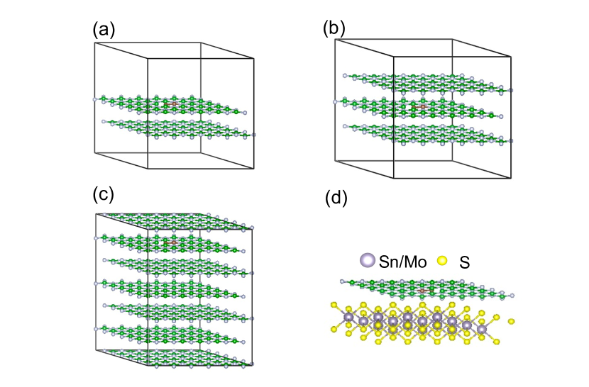
We next look at the layer thickness dependence and substrate effects on defect emitter properties. We use our implicit -sum method [46, 47] to calculate properties of one isolated defect within 1-3 layers (Fig.4(a-b)) and bulk hBN (Fig.4(c)). We choose the AA’ stacking structure and set the inter-layer distance to the bulk value of of 3.33 Å [56]. For the substrate effect study, we choose two different transition metal dichalcogenides (TMD) materials as substrates (Fig.4(d)) with layer distance to defective hBN 3.31 Å for and 3.33 Å for substrates [46].
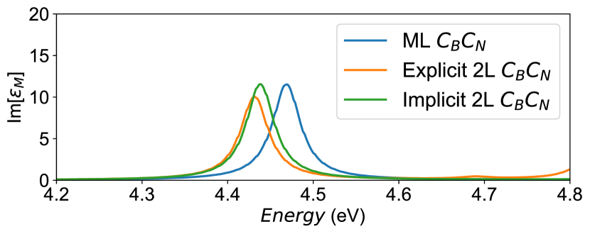
To validate the result from our implicit -sum method [46, 47], we compare its results with explicit bilayer calculations by using in hBN as an example. In Fig.5, the panel above is the BSE absorption spectrum of defect-related peaks, where we show the explicit (orange) and implicit (green) two-layer calculations give similar results for carbon-dimer defect, which are both red-shifted by 0.03 eV compared to the monolayer one (blue). The table below summarizes the excitation energy (), electronic gap (), and radiative lifetime () of the defect emitter, calculated from explicit and implicit interface methods.
| (eV) | (ns) | (eV) | (eV) | |
|---|---|---|---|---|
| ML | 4.469 | 1.1 | 6.336 | 1.867 |
| Implicit | 4.438 | 1.3 | 6.045 | 1.607 |
| Explicit | 4.431 | 1.3 | 5.958 | 1.527 |
| Error(Im.-Ex.) | 0.007 | 0.087 | 0.080 |
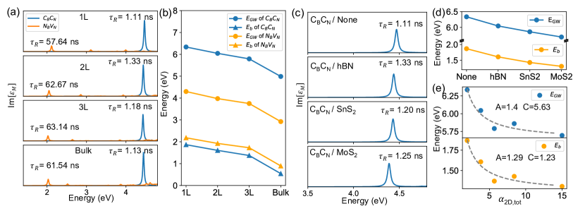
We then show the results of layer thickness and substrate effects on optical spectra by using implicit -sum method in Fig.6 (a) and (c). With increasing the number of layers or adding substrates, the position of defect peaks remains nearly constant, with tiny shift (within 80 meV).
The radiative lifetime () also has negligible change. This result is consistent with experimental observations, where defect emitters did not change its ZPL energy either from 1L to 5L or with various substrates [57].
In Fig.6(b) and (d) we show the layer thickness and substrate effect on GW energy gap () and exciton binding energy() of intra-defect transitions. A monotonic decrease of both and has been observed as increasing layer thickness, where the change nearly cancels each other, leaving the optical excitation energy unchanged ().
Interestingly, the substrate/layer effects on two defect emitters are similar; e.g. for , decreases by 1.348 eV from monolayer to bulk, and for it decreases by 1.370 eV.
This finding indicates that the defect state energy renormalization by layer thickness and substrates weakly depends on the specific defects, but is mostly determined by the host environment.
We then qualitatively show that the energy renormalization of and of defects is directly related to the environmental dielectric screening surrounding the defects, represented by total 2D effective polarizability () [58, 59]. can be calculated by summing up the 2D effective polarizability from each subsystem (; “sub” denotes substrate and “def” denotes defected hBN monolayer), where the 2D effective polarizability of the subsystem is obtained by . Here is the supercell lattice constant along the out-of-plane direction, and is the in-plane component of macroscopic dielectric tensor of the substrate calculated by Density Functional Perturbation Theory (DFPT) [60] (The dielectric constants are listed in SI). We then use equation to fit the relation between and /, with and the fitting parameters. The results are plotted in Fig.6(e), which shows the inversely proportional relation can well describe the and dependence on environmental screening surrounding the defects (from both host hBN and substrates).
To better understand the insensitivity of defect optical transition towards environmental screening, we present an analytic model for analyzing the renormalization of the defects’ exciton binding energy (). Our analysis suggests that the stability of the defect spectroscopic peak position against the layer thickness and substrate is a result of two factors: (i) the high localization of the defect wave function and (ii) the defect-related optical transition with no mixing with other transition involving delocalized wave function from the host, as discussed in detail below.
We start with the Hamiltonian for Bethe-Salpeter equation in Wannier basis [61]:
| (4) |
where are the pairs of occupied and unoccupied states, is the real-space lattice site, is the spin, is the screened exchange interaction between electron and hole (the direct term), is the exchange term from the Hartree potential, and is the GW electronic energy gap between and states. The Wannier function basis is obtained from the Fourier Transform of the reciprocal-space Kohn Sham wave function to the real-space lattice :
| (5) |
The exciton energy and wavefunctions are obtained by diagonalizing the Hamiltonian:
| (6) |
where is the of exciton wavefunction and is the exciton energy.
We consider the perturbation from the dielectric screening of pristine substrates or other pristine host material layers. (Notice that the in-homogeneous local dielectric environment from the host material around the defect is part of the unperturbed Hamiltonian.) The first order perturbed change to the exciton energy is then:
| (7) | |||||
where the matrix element of perturbed Hamiltonian is:
| (8) | |||||
in which the first term is the renormalization of electronic gap between the pair of c/v states. The second term is the change of screened exchange interaction, which contributes to the exciton binding energy change , defined as follows:
| (9) | |||||
Since the exchange term from the Hartree potential does not depend on dielectric screening, it does not appear in the perturbative Hamiltonian.
Here we consider defect related Frenkel-like excitons, whose wavefunctions usully have components only from defect states, i.e the is nonzero only when c and v are defect states. The previous study on the GW band gap renormalization effect of dielectric screening on benzene systems [62](with COHSEX model) has suggest that, when is smooth and slowly varying over the spacial extension of the orbital, the GW energy gap renormalization can be approximated by , where is the static polarization integral for c/v state,
| (10) |
When defect orbitals are highly localized in real space, the integration can be reduce to the classical limit, where [63, 62].
The same argument can be applied to the second term in Eq. 7, where the matrix element of two particle screened Coulomb interaction change can be written as
| . | (11) |
Since a single defect is not subject to a spacial periodicity, we can ignore the inter-site interaction and set =0. Then we rewrite the equation with two-electrons’ distance , assuming the substrate screening being homogeneous in-plane (which is a reasonable approximation according to our past work [46]),
| (12) |
Given localized (Frenkel) exciton, is rather small or exciton wavefunction is spatially confined. With orthonormal condition of single-particle wavefunctions, we have
| (13) | |||||
Combining the discussions above on both terms in Eq.8, we have the when and are both defect single-particle states. Thus, the Frenkel-like exciton, composed by localized defect-defect transitions, will experience no change at presence of substrate screening.
At last, we apply a static model for derived from image charges [63] and compare with ab-initio GW/BSE results. The environmental screening potential can be modeled as the potential energy of two charges in the defect layer (with dielectric constant ) on top of substrate (with dielectric constant ) [63]. We assume the region above the defect layer to be a vacuum.
| (14) |
where is the thickness of the defect layer, and . We use the monolayer defect system without any substrate () as the reference, then is defined as the change of with and without substrates:
| (15) |
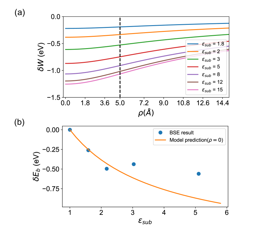
We plotted the change of screened Coulomb potential, in Fig. 7 (a), where the defect layer thickness is extracted from inter-layers distance, and defect layer dielectric constant is obtained in SI section V. The dashed line at 5 represents the maximum spanning range of the localized defect states and .
Fig. 7(b) shows that the calculated by Eq. 9, Eq. 14, and Eq. 15 compares reasonably well with ab-initio BSE calculations (blue dots), especially in low substrate screening regime. The underestimation of at the high dielectric constant of substrates range may be due to an over-simplification of model in Eq. 14. Nevertheless, the full ab-initio GW/BSE calculation suggests that the cancellation effect for defect state transitions between exciton binding energy () and GW quasiparticle energy renormalization () still holds even at high substrate dielectric screening.
IV Conclusions
In this work, we have explored the impact of strain, layer thickness, and substrate effects on the electronic and optical properties of point defects in 2D insulator - hexagonal boron nitride (hBN). Our investigation takes into account the effects of many-body interaction and excited-state relaxation. We first analyzed various contributions to strain susceptibility of ZPL, and found the dominant contributions often stem from the changes at the single-particle level. We explained the ZPL shift direction under strain through molecular orbital theory, which is defect dependent, relying on the chemical bonding nature at the defect center.
Next our ab-initio calculations demonstrate the robustness of optical peak position of defect single photon emitters (SPEs) when varying number of layers and substrates. We reveal the perfect cancellation between the renormalization of quasiparticle energy gap and exciton binding energy due to environmental screening. To further understand this result, we derived analytical models based on solving BSE with Wannier basis for Frenkel excitons, to reveal the underlying mechanism and the required condition, i.e. the localization nature of defect bound exciton. We then use simple image-charge model for screened Coulomb potential to further validate such cancellation effect.
Our findings provide in-depth insights of mechanism and conditions that control the environmental impact on the properties of quantum defects, and shine light on the emerging research on strain and substrate engineering of quantum defects in 2D materials.
Acknowledgements.
We acknowledge the support by the National Science Foundation under grant no. DMR-2143233. This research used resources of the Scientific Data and Computing center, a component of the Computational Science Initiative, at Brookhaven National Laboratory under Contract No. DE-SC0012704, the lux supercomputer at UC Santa Cruz, funded by NSF MRI grant AST 1828315, the National Energy Research Scientific Computing Center (NERSC) a U.S. Department of Energy Office of Science User Facility operated under Contract No. DE-AC02-05CH11231, the Extreme Science and Engineering Discovery Environment (XSEDE) which is supported by National Science Foundation Grant No. ACI-1548562 [64].References
- Aharonovich and Toth [2017] I. Aharonovich and M. Toth, Sci. 358, 170 (2017).
- Liu and Hersam [2019] X. Liu and M. C. Hersam, Nat. Rev. Mater. 4, 669 (2019).
- Wolfowicz et al. [2021] G. Wolfowicz, F. J. Heremans, C. P. Anderson, S. Kanai, H. Seo, A. Gali, G. Galli, and D. D. Awschalom, Nat. Rev. Mater. 6, 906 (2021).
- Yim et al. [2020] D. Yim, M. Yu, G. Noh, J. Lee, and H. Seo, ACS Appl. Mater. Interfac. 12, 36362 (2020).
- Li et al. [2020] S. Li, J.-P. Chou, A. Hu, M. B. Plenio, P. Udvarhelyi, G. Thiering, M. Abdi, and A. Gali, npj Quantum Inf 6, 1 (2020).
- Mendelson et al. [2020] N. Mendelson, M. Doherty, M. Toth, I. Aharonovich, and T. T. Tran, Advanced Materials 32, 1908316 (2020).
- Tran et al. [2016a] T. T. Tran, K. Bray, M. J. Ford, M. Toth, and I. Aharonovich, Nat. Nanotechnol. 11, 37 (2016a).
- Gottscholl et al. [2020] A. Gottscholl, M. Kianinia, V. Soltamov, S. Orlinskii, G. Mamin, C. Bradac, C. Kasper, K. Krambrock, A. Sperlich, M. Toth, et al., Nat. Mater. 19, 540 (2020).
- Gottscholl et al. [2021] A. Gottscholl, M. Diez, V. Soltamov, C. Kasper, A. Sperlich, M. Kianinia, C. Bradac, I. Aharonovich, and V. Dyakonov, Sci. Adv. 7, eabf3630 (2021).
- Gao et al. [2022] X. Gao, S. Vaidya, K. Li, P. Ju, B. Jiang, Z. Xu, A. E. L. Allcca, K. Shen, T. Taniguchi, K. Watanabe, et al., arXiv preprint arXiv:2203.13184 (2022).
- Qian et al. [2022] C. Qian, V. Villafañe, M. Schalk, G. V. Astakhov, U. Kentsch, M. Helm, P. Soubelet, N. P. Wilson, R. Rizzato, S. Mohr, et al., arXiv preprint arXiv:2202.10980 (2022).
- Reimers et al. [2020] J. R. Reimers, J. Shen, M. Kianinia, C. Bradac, I. Aharonovich, M. J. Ford, and P. Piecuch, Phys. Rev. B 102, 144105 (2020).
- Ivády et al. [2020] V. Ivády, G. Barcza, G. Thiering, S. Li, H. Hamdi, J.-P. Chou, Ö. Legeza, and A. Gali, npj Comput. Mater. 6, 1 (2020).
- Grosso et al. [2017a] G. Grosso, H. Moon, B. Lienhard, S. Ali, D. K. Efetov, M. M. Furchi, P. Jarillo-Herrero, M. J. Ford, I. Aharonovich, and D. Englund, Nat. Commun. 8, 705 (2017a).
- Mendelson et al. [2021] N. Mendelson, D. Chugh, J. R. Reimers, T. S. Cheng, A. Gottscholl, H. Long, C. J. Mellor, A. Zettl, V. Dyakonov, P. H. Beton, et al., Nat. Mater. 20, 321 (2021).
- Bourrellier et al. [2016] R. Bourrellier, S. Meuret, A. Tararan, O. Stéphan, M. Kociak, L. H. Tizei, and A. Zobelli, Nano Lett. 16, 4317 (2016).
- Museur et al. [2008] L. Museur, E. Feldbach, and A. Kanaev, Phys. Rev. B 78, 155204 (2008).
- Turiansky et al. [2019] M. E. Turiansky, A. Alkauskas, L. C. Bassett, and C. G. Van de Walle, Phys. Rev. Lett. 123, 127401 (2019).
- Sajid and Thygesen [2020] A. Sajid and K. S. Thygesen, 2D Mater. 7, 031007 (2020).
- Fischer et al. [2021] M. Fischer, J. Caridad, A. Sajid, S. Ghaderzadeh, M. Ghorbani-Asl, L. Gammelgaard, P. Bøggild, K. S. Thygesen, A. Krasheninnikov, S. Xiao, et al., Sci. Adv. 7, eabe7138 (2021).
- Jara et al. [2021] C. Jara, T. Rauch, S. Botti, M. A. Marques, A. Norambuena, R. Coto, J. Castellanos-Águila, J. R. Maze, and F. Munoz, J. Phys. Chem. A 125, 1325 (2021).
- Li et al. [2022a] K. Li, T. J. Smart, and Y. Ping, Phys. Rev. Mater. 6, L042201 (2022a).
- Golami et al. [2022] O. Golami, K. Sharman, R. Ghobadi, S. C. Wein, H. Zadeh-Haghighi, C. G. da Rocha, D. R. Salahub, and C. Simon, Phys. Rev. B 105, 184101 (2022).
- Maciaszek et al. [2022] M. Maciaszek, L. Razinkovas, and A. Alkauskas, Phys. Rev. Mater. 6, 014005 (2022).
- Mackoit-Sinkevičienė et al. [2019] M. Mackoit-Sinkevičienė, M. Maciaszek, C. G. Van de Walle, and A. Alkauskas, Appl. Phys. Lett. 115, 212101 (2019).
- Vokhmintsev et al. [2019] A. Vokhmintsev, I. Weinstein, and D. Zamyatin, J. Lumin. 208, 363 (2019).
- Hamdi et al. [2020] H. Hamdi, G. Thiering, Z. Bodrog, V. Ivády, and A. Gali, npj Comput. Mater. 6, 1 (2020).
- Li et al. [2022b] S. Li, A. Pershin, G. Thiering, P. Udvarhelyi, and A. Gali, J. Phys. Chem. Lett. 13, 3150 (2022b).
- Tran et al. [2016b] T. T. Tran, C. Elbadawi, D. Totonjian, C. J. Lobo, G. Grosso, H. Moon, D. R. Englund, M. J. Ford, I. Aharonovich, and M. Toth, ACS nano 10, 7331 (2016b).
- Krečmarová et al. [2021] M. Krečmarová, R. Canet-Albiach, H. Pashaei-Adl, S. Gorji, G. Muñoz-Matutano, M. Nesládek, J. P. Martínez-Pastor, and J. F. Sánchez-Royo, ACS Appl. Mater. Interfac. 13, 46105 (2021).
- Wu et al. [2019a] F. Wu, T. J. Smart, J. Xu, and Y. Ping, Phys. Rev. B 100, 081407(R) (2019a).
- Dev [2020] P. Dev, arXiv preprint arXiv:2002.05098 (2020).
- Ping and Smart [2021] Y. Ping and T. J. Smart, Nat Comput Sci 1, 646 (2021).
- Amblard et al. [2022] D. Amblard, G. D’Avino, I. Duchemin, and X. Blase, arXiv:2204.11671 [cond-mat] (2022), arXiv:2204.11671 [cond-mat] .
- Wang and Sundararaman [2020] D. Wang and R. Sundararaman, Phys. Rev. B 101, 054103 (2020).
- Wang and Sundararaman [2019] D. Wang and R. Sundararaman, Phys. Rev. Materials 3, 083803 (2019).
- Giannozzi et al. [2009] P. Giannozzi, S. Baroni, N. Bonini, M. Calandra, R. Car, C. Cavazzoni, D. Ceresoli, G. L. Chiarotti, M. Cococcioni, I. Dabo, A. Dal Corso, S. de Gironcoli, S. Fabris, G. Fratesi, R. Gebauer, U. Gerstmann, C. Gougoussis, A. Kokalj, M. Lazzeri, L. Martin-Samos, N. Marzari, F. Mauri, R. Mazzarello, S. Paolini, A. Pasquarello, L. Paulatto, C. Sbraccia, S. Scandolo, G. Sclauzero, A. P. Seitsonen, A. Smogunov, P. Umari, and R. M. Wentzcovitch, J. Phys.: Condens. Matter 21, 395502 (2009).
- Perdew et al. [1996] J. P. Perdew, K. Burke, and M. Ernzerhof, Phys. Rev. Lett. 77, 3865 (1996).
- Schlipf and Gygi [2015] M. Schlipf and F. Gygi, Computer Physics Communications 196, 36 (2015).
- Hamann [2013] D. R. Hamann, Phys. Rev. B 88, 085117 (2013).
- Smart et al. [2021] T. J. Smart, K. Li, J. Xu, and Y. Ping, npj Comput Mater 7, 1 (2021).
- Ping et al. [2013] Y. Ping, D. Rocca, and G. Galli, Chem. Soc. Rev. 42, 2437 (2013).
- Marini et al. [2009] A. Marini, C. Hogan, M. Grüning, and D. Varsano, Computer Physics Communications 180, 1392 (2009).
- Rozzi et al. [2006] C. A. Rozzi, D. Varsano, A. Marini, E. K. U. Gross, and A. Rubio, Phys. Rev. B 73, 205119 (2006).
- Wu et al. [2019b] F. Wu, D. Rocca, and Y. Ping, J. Mater. Chem. C 7, 12891 (2019b).
- Guo et al. [2020] C. Guo, J. Xu, D. Rocca, and Y. Ping, Phys. Rev. B 102, 205113 (2020).
- Guo et al. [2021] C. Guo, J. Xu, and Y. Ping, J. Phys.: Condens. Matter 33, 234001 (2021).
- Mackoit-Sinkevičienė et al. [2019] M. Mackoit-Sinkevičienė, M. Maciaszek, C. G. Van de Walle, and A. Alkauskas, Appl. Phys. Lett. 115, 212101 (2019).
- Wu et al. [2019c] F. Wu, T. J. Smart, J. Xu, and Y. Ping, Phys. Rev. B 100, 081407 (2019c).
- Winter et al. [2021] M. Winter, M. H. E. Bousquet, D. Jacquemin, I. Duchemin, and X. Blase, Phys. Rev. Materials 5, 095201 (2021).
- Abdi et al. [2018] M. Abdi, J.-P. Chou, A. Gali, and M. B. Plenio, ACS Photonics 5, 1967 (2018).
- Gao et al. [2021] S. Gao, H.-Y. Chen, and M. Bernardi, npj Comput Mater 7, 85 (2021).
- Hayee et al. [2020] F. Hayee, L. Yu, J. L. Zhang, C. J. Ciccarino, M. Nguyen, A. F. Marshall, I. Aharonovich, J. Vučković, P. Narang, T. F. Heinz, and J. A. Dionne, Nat. Mater. 19, 534 (2020).
- Grosso et al. [2017b] G. Grosso, H. Moon, B. Lienhard, S. Ali, D. K. Efetov, M. M. Furchi, P. Jarillo-Herrero, M. J. Ford, I. Aharonovich, and D. Englund, Nat Commun 8, 705 (2017b).
- Xue et al. [2018] Y. Xue, H. Wang, Q. Tan, J. Zhang, T. Yu, K. Ding, D. Jiang, X. Dou, J.-j. Shi, and B.-q. Sun, ACS Nano 12, 7127 (2018).
- Hod [2012] O. Hod, J. Chem. Theory Comput. 8, 1360 (2012).
- Krečmarová et al. [2021] M. Krečmarová, R. Canet Albiach, H. Pashaei Adl, S. Gorji, G. Muñoz-Matutano, M. Nesladek, J. Martínez-Pastor, and J. F. Sánchez Royo, ACS Applied Materials & Interfaces 13, 46105 (2021).
- Molina-Sánchez et al. [2020] A. Molina-Sánchez, G. Catarina, D. Sangalli, and J. Fernández-Rossier, J. Mater. Chem. C 8, 8856 (2020).
- Tian et al. [2020] T. Tian, D. Scullion, D. Hughes, L. H. Li, C.-J. Shih, J. Coleman, M. Chhowalla, and E. J. G. Santos, Nano Lett. 20, 841 (2020).
- Baroni et al. [2001] S. Baroni, S. de Gironcoli, A. Dal Corso, and P. Giannozzi, Rev. Mod. Phys. 73, 515 (2001).
- Bechstedt [2015] F. Bechstedt, Many-Body Approach to Electronic Excitations, Springer Series in Solid-State Sciences, Vol. 181 (Springer Berlin Heidelberg, Berlin, Heidelberg, 2015).
- Neaton et al. [2006] J. B. Neaton, M. S. Hybertsen, and S. G. Louie, Phys. Rev. Lett. 97, 216405 (2006).
- Cho and Berkelbach [2018] Y. Cho and T. C. Berkelbach, Phys. Rev. B 97, 041409 (2018).
- Towns et al. [2014] J. Towns, T. Cockerill, M. Dahan, I. Foster, K. Gaither, A. Grimshaw, V. Hazlewood, S. Lathrop, D. Lifka, G. D. Peterson, R. Roskies, J. R. Scott, and N. Wilkins-Diehr, Comput. Sci. Eng. 16, 62 (2014).