Coupled Ferroelectricity and Superconductivity in Bilayer -MoTe2
Abstract
Achieving electrostatic control of quantum phases is at the frontier of condensed matter research. Recent investigations have revealed superconductivity tunable by electrostatic doping in twisted graphene heterostructures and in two-dimensional (2D) semimetals such as WTe2 [1, 2, 3, 4, 5]. Some of these systems have a polar crystal structure that gives rise to ferroelectricity, in which the interlayer polarization exhibits bistability driven by external electric fields [6, 8, 7]. Here we show that bilayer -MoTe2 simultaneously exhibits ferroelectric switching and superconductivity. Remarkably, a field-driven, first-order superconductor-to-normal transition is observed at its ferroelectric transition. Bilayer -MoTe2 also has a maximum in its superconducting transition temperature () as a function of carrier density and temperature, allowing independent control of the superconducting state as a function of both doping and polarization. We find that the maximum is concomitant with compensated electron and hole carrier densities and vanishes when one of the Fermi pockets disappears with doping. We argue that this unusual polarization-sensitive 2D superconductor is driven by an interband pairing interaction associated with nearly nested electron and hole Fermi pockets.
Department of Physics, Columbia University, New York, NY, USA
School of Physics and Astronomy, University of Minnesota, Minneapolis, MN, USA
Department of Chemical Engineering and Materials Science, University of Minnesota, Minneapolis, MN, USA
Department of Materials Science and Engineering, University of Wisconsin, Madison, WI, USA
National Institute for Materials Science, Tsukuba, Japan
Department of Mechanical Engineering, Columbia University, New York, NY, USA
Correspondence to: apn2108@columbia.edu, darhodes@wisc.edu
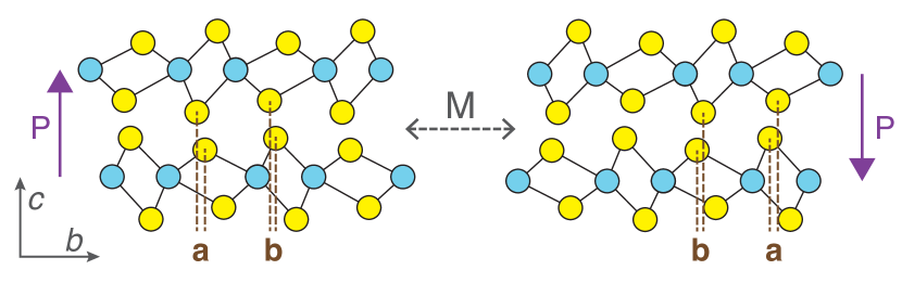
Ferroelectricity has been recently found in a number of two-dimensional (2D) van der Waals layered heterostructures that break inversion symmetry either intrinsically [7, 8] or through heterostructure engineering [6]. In contrast to traditional ferroelectricity that arises due to long range Coulomb interactions in compounds such as BaTiO3[9], this phenomenon is thought to emerge due to the interplay between interlayer sliding and the small dipole moments arising from broken inversion symmetry. For instance, in bilayer hBN, out-of-plane electric fields can cause interlayer sliding, changing the stacking order from BA to AB and switching the polarization direction[10]. The same principle has been extended to rhombohedral-stacked bilayer transition metal dichalcogenides (TMDs) [11, 12], and orthorhombic-stacked bilayer -WTe2[7, 8], demonstrating a viable path to achieving ferroelectric behavior in almost any noncentrosymmetric 2D heterostructure. Compared to thin film oxides (e.g., BiFeO3)[13], ferroelectric 2D heterostructures offer compelling advantages: tunable electronic behavior via conventional electrostatic techniques, modifications through strain, and the ability to exploit ferroelectricity to control other electronic states. Importantly, because 2D ferroelectric structures are atomically thin, in-plane metallic states are compatible with the out-of-plane polarization[8]. For example, several metallic TMDs show 2D superconductivity at low temperatures[14, 15, 16]. Ferroelectricity thus offers another tuning knob, besides electrostatic doping, to control and assess 2D superconductivity. A possible candidate to achieve this goal is few-layer -MoTe2 (hereafter referred to as MoTe2), which has been independently shown to display ferroelectricity and compensated superconductivity [17, 16].
In the bulk, MoTe2 is a nearly compensated semimetal[18, 19] with a superconducting of 100 mK [20, 21]. Density functional theory (DFT) calculations suggest that monolayer[16] and bilayer MoTe2 (see Fig. 1b) retain this charge compensated behavior, displaying nearly compensated electron and hole pockets at the Fermi level with a small bilayer splitting. The superconducting transition temperature unusually increases with decreasing thickness, reaching a maximum of 7 K in the monolayer limit[16]. This behavior is distinctly different from other 2D superconductors, where superconductivity is dominated by a single carrier type, such as monolayer WTe2[4, 5] or few-layer NbSe2[22]. MoTe2 also takes on a polar crystal structure, where net out-of-plane polarization arises between layers in the few-layer limit. This polarization, along with its out-of-plane switching, has been previously demonstrated via piezoresponse force microscopy measurements [17]. The switching behavior, similar to that seen in WTe2, has been attributed to interlayer sliding[4, 5]. Assuming this to be the case, bilayer MoTe2 is the thinnest possible material that still has the sliding degree of freedom present, and we use it as a platform to study the interaction between the superconducting state and the electric polarization.
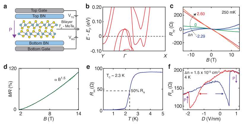
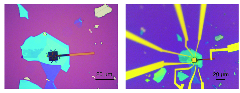
For our experiments, we fabricate bilayer MoTe2 samples with dual top and bottom gate electrodes whose voltages and allow us to tune carrier-density, , and displacement field, , independently (Fig. 1a and Supplementary Fig. 2). Shown in Fig. 1c are measurements of the Hall resistance at 250 mK for several different carrier densities. The data at low clearly shows that the Hall effect is nonlinear in field. As we increase , we see the Hall signal evolve from a nonlinear to linear, suggesting a single dominant carrier at high (a full discussion of the Hall effect in our device is provided in Supplementary Information (SI)). We also see a non-saturating magnetoresistance at zero doping in our samples, also shown in Fig. 1d. All of these features are hallmarks of compensated semimetals[1, 26, 27]. These measurements are, therefore, broadly consistent with the expected electronic structure of pristine material from density functional theory (DFT) calculations. This agreement indicates that there is no large external doping or degradation present in our bilayer samples.
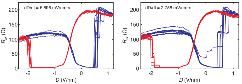
Figure 1e shows the resistance of the undoped sample as a function of temperature. A clear superconducting transition is observed, with a of 2.3 K [16]. In order to probe the presence of ferroelectricity, we sweep at a fixed density in the normal state (4 K). We observe hysteretic switching of the four-probe resistance, Rxx, as shown in Fig. 1f. While such resistive switching has not previously been observed in MoTe2, it has been seen in multilayered WTe2 [7, 8]. In analogy with WTe2, we associate this resistance bistability with an interlayer sliding transition, which flips the out-of-plane polarization[4, 5].
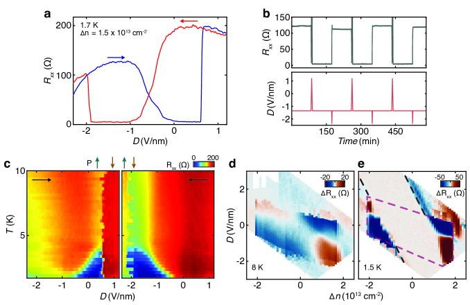
To study how the ferroelectricity interacts with 2D superconductivity at low temperatures, we measure as a function of displacement field at 1.7 K, as shown in Fig. 2a. We clearly observe the presence of both superconductivity and hysteretic switching due to ferroelectricity. Starting from V/nm (blue curve, Fig. 2a), both the displacement field and the sample polarization point in the same direction. On decreasing the magnitude of the displacement field and then flipping its sign, superconductivity emerges gradually - resulting in a drop of the sample resistance to zero. The sample remains superconducting until the displacement field switches the crystal’s internal polarization, at which point it transitions to the normal state. The behavior on the downward sweep of displacement field is similar, with the hysteresis expected from the ferroelectricity. The asymmetry of the superconducting butterfly loop with applied field has been seen in other van der Waals ferroelectrics[7, 8, 10]. Its origin is likely extrinsic to the material itself and is possibly related to substrate and contact asymmetries.
The coexistence of ferroelectric switching and superconductivity in a single material can be used to make a superconducting switch driven by external electric field. We illustrate this in Fig 2b, which shows the resistance of the sample as a function of time as external fields are applied to the sample. Starting from the normal (superconducting) state, an electric field pulse of appropriate positive (negative) sign can drive a transition to the superconducting (normal) phase. Once the switching between states is established, the resistance of the sample continues to stay in the new state indefinitely, as is seen in the figure. Such a first-order switch for superconductivity may lead to low-temperature classical and quantum electronics applications, such as low-power transistors and tunable qubits in the future.
In order to explore the connection between ferroelectric switching and superconductivity more carefully, we perform displacement field sweeps at different temperatures, the results of which are summarized in Fig. 2c for the two sweep directions. For the forward direction, as the displacement field is lowered from a high absolute value to a low value, a superconducting transition emerges at low temperatures. On continuing to sweep the displacement field through zero, continues to increase until the displacement field switches the polarization, at which point superconductivity is lost. In both sweep directions, the maximum is therefore seen just before a switching event. This continuous tuning of prior to switching shows that the mechanism for the superconducting state is intimately tied to the internal electric field of the sample.
The ferroelectric switching behavior described above is density dependent, as is the observed superconducting behavior. In order to understand the region of ferroelectricity in the carrier doping versus displacement field phase diagram, we perform sweeps of the displacement field similar to Fig. 2a at various doping levels, both in the superconducting state and in the normal state. Taking the difference in resistance between the forward and backward sweep directions identifies when hysteretic switching is observed in the samples. Shown in Fig. 2d are the results of such measurements in the normal state ( = 8 K) and in the superconducting state ( = 1.5 K). Focusing on the normal state, we observe that the hysteretic switching in our samples is limited to a doping range of cm-2 in our measurements. Such switching behavior is observed up to 60 K (see SI). Whether the absence of ferroelectric switching at high doping is an intrinsic effect or whether it is due to constraints of the gate voltages we can achieve in our experiment is currently unclear.
The corresponding measurements in the superconducting state clearly show the role of the internal electric field in the observed superconducting behavior. In general, we observe that electric field can drive a superconducting transition in the sample both at low and high doping (black dashed lines, Fig. 2e). We see that hysteretic superconductivity occurs in parts of the phase diagram that are close to the boundary where field-driven superconductivity intersects with the normal state ferroelectric behavior. This phenomenology suggests the simple hypothesis that it is the total internal electric field in the sample that controls superconductivity: the sample polarization, when flipped, can turn the superconducting phase on or off if sufficiently close to the field-driven superconducting transition.
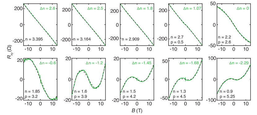
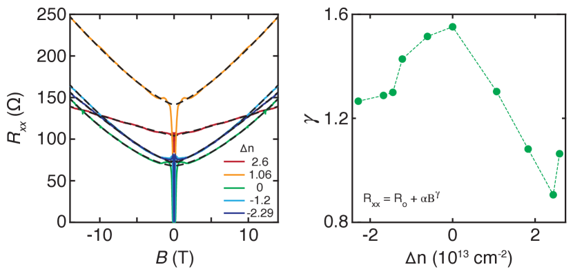
So far, we have discussed the displacement field dependent properties of the sample. Now, we turn to the carrier density dependence of superconductivity in the sample at zero displacement field. Shown in Fig. 3a is a color plot of the temperature-dependent resistance of the sample that shows the presence of a maximum in of 2.5 K. By fitting the Hall measurements in Fig. 1c with a two-band semiclassical model (see SI for details), we extract the independent electron and hole carrier densities of the bilayer (Fig. 3b). This plot shows that the maximum is closely correlated to the compensation point of the material, . To further confirm our Hall analysis and the compensated behavior, we measure the magnetoresistance as a function of doping. In agreement with the two-band model, we see a non-saturating magnetoresistance for and for intermediate values of where both electron and holes bands cross the Fermi level (see SI).
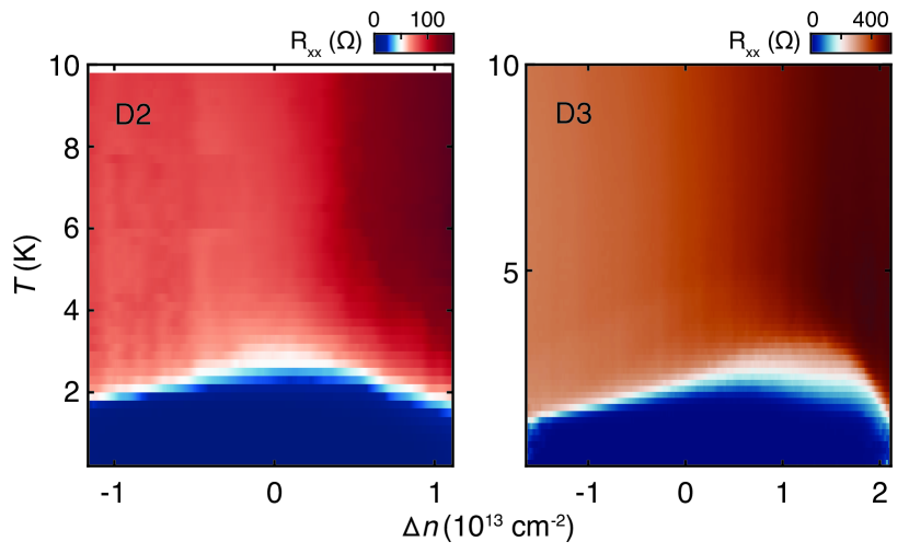
Upon doping with electrons we see an overall reduction in until is reached, beyond which superconductivity disappears completely (down to 250 mK). This complete suppression of superconductivity occurs at the same concentration where the Hall effect becomes linear and the magnetoresistance saturates with increasing magnetic field. Therefore, superconductivity disappears when the chemical potential is raised above the hole pocket. While the same trend is seen upon doping with holes, we cannot suppress superconductivity completely since we are limited in the voltage we can safely apply to our gates. The main finding that is maximized near the compensation point is reproduced in multiple devices (see Extended Data Fig. 1), but the precise shape of the versus doping curve shows device to device variations.
At zero displacement field, it is clear from the discussion above that both hole and electron carriers are required to maximize superconductivity. We can ask whether the same is true when hysteretic superconducting switching is observed. To study this, we measure the Hall effect in the region of ferroelectric hysteresis at . Shown in Fig. 3c are a subset of this data as the displacement field is swept from right to left (left panel) and from left to right (right panel). The curves are color-coded for different displacement field values according to the symbols in Fig. 3d. Starting from high positive displacement field, where the sample is in the normal state, the Hall resistance is linear in field and is well-fitted using a single electron band model. As we sweep the field down and enter the superconducting state, the Hall effect develops a pronounced nonlinearity and shows the presence of both types of carriers. Upon switching out of the superconducting state at large negative field, the Hall effect goes back to nearly linear, showing that the hole carrier density is sharply reduced. The same trend is seen when sweeping the field back from negative to positive values, with a non-linear Hall effect seen where the sample is superconducting. The extracted carrier concentrations are shown in Fig. 3d, with the hysteretic superconducting regions shaded in red (for the sweep from right to left) and in blue (from left to right). The observation that we need both types of carriers to have superconductivity is clearly seen from this figure.
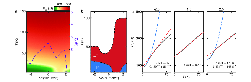
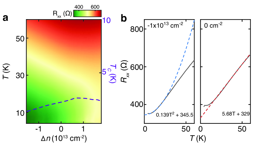
To further investigate the metallic state from which 2D superconductivity emerges, we measure the temperature dependence of the normal state resistance at various doping levels and zero displacement field, as shown in Extended Data Fig. 2 a,b. In bulk MoTe2, the temperature dependence of the resistance is up to 50 K, after which it becomes dominated by phonon scattering[28]. On the other hand, for bilayer MoTe2, we observe an approximately linear-in- resistance for intermediate temperatures. For most doping values, the resistance recovers the usual dependence at low temperatures, as shown in Extended Data Fig. 2c. However, as summarized in extended data Fig. 2c, for a narrow range of near the edge of the superconducting dome, the -linear behavior persists down to the superconducting . This behavior has been qualitatively reproduced in at least one other device (see Extended Data Fig. 3). In certain unconventional superconductors[29, 30] and other 2D correlated systems[31, 32], a -linear resistance is often associated with an underlying strange metallic state, whose origin remains widely debated. In the present case of bilayer MoTe2, it is important to notice that the -linear contribution is comparable to the residual resistance.
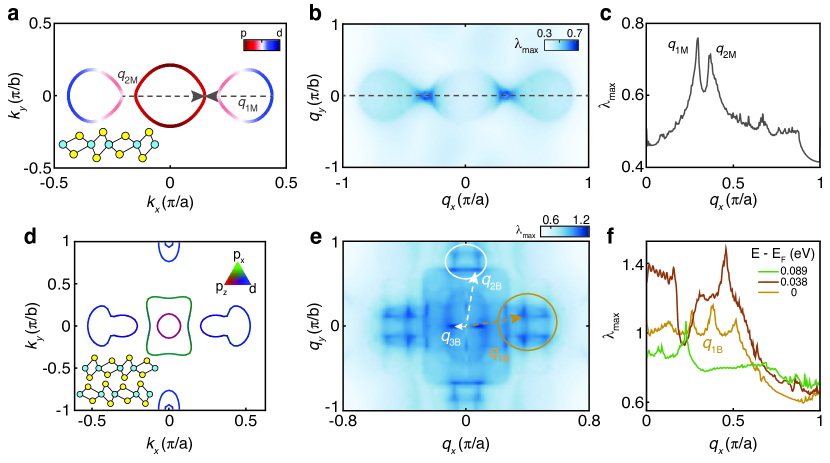
The fact that superconductivity appears only when both electron and hole pockets are present suggests that interband processes are behind the pairing mechanism. The situation is reminiscent of iron-pnictide superconductors, which are also compensated semimetals [33]. In that case, the pairing interaction has been proposed to be enhanced by spin fluctuations. Interestingly, prior results on monolayer MoTe2 hypothesized that the enhancement in was unconventional and likely related to enhanced spin fluctuations[16]. To further analyze this scenario, we compute the leading eigenvalue of the multi-orbital Lindhard susceptibility from DFT calculations (see Methods for details). To set the stage, we first consider the monolayer case, whose Fermi surface is shown in Fig. 4a. As seen in Figs. 4b-c, is peaked at the two nesting wave-vectors and that connect the edges of the electron and hole pockets along the axis.
The situation in bilayer MoTe2 is slightly more complicated due to the presence of an additional electron pocket along the direction as well as the bilayer splitting (Fig. 4d). As a result, displays a peak not only at the nesting wave-vector, , connecting the hole and electron pockets approximately along , but also at the wave-vector, , connecting the hole and electron pockets along (Fig. 4e). Moreover, an additional peak appears at , which connects the bilayer-split hole pockets. Electron-electron interactions involving the same or different orbitals are expected to enhance one or more of these peaks, thus providing a possible mechanism for the interband pairing interaction. This would imply that MoTe2 is a rather unusual 2D superconductor. While other mechanisms cannot be ruled out at present, this simple nesting-driven scenario is qualitatively consistent with the doping dependence of observed in bilayer MoTe2. Indeed, as shown in Fig. 4f, the peak of at first increases for small electron doping and then decreases and disappears once the hole pocket is pushed down below the Fermi level.
Our finding of a tunable in the ferroelectric regime of bilayer MoTe2 shows that this material is a promising platform for controlling an unusual type of 2D superconductivity with two independent and highly-precise knobs: doping and displacement field. At the same time, the discrete switching of superconductivity at the ferroelectric transition opens up new possibilities for quantum devices with a first order switch for the superconducting phase. We expect that these effects will have interesting dependence on layer thickness[7] and twist angle that tunes the degree of inversion symmetry breaking[10]. Such effects should also be present in other noncentrosymmetric 2D superconductors[34]. Finally, the control of these properties using ultrafast electromagnetic excitations that couple to the lattice is also an appealing prospect [35, 36].
References
References
- [1] Cao, Y. et al. Unconventional superconductivity in magic-angle graphene superlattices. Nature 556, 43–50 (2018).
- [2] Liu, X. et al. Tunable spin-polarized correlated states in twisted double bilayer graphene. Nature 583, 221–225 (2020).
- [3] Park, J.M. et al. Tunable strongly coupled superconductivity in magic-angle twisted trilayer graphene. Nature 590, 249–255 (2021).
- [4] Fatemi, V. et al. Electrically tunable low-density superconductivity in a monolayer topological insulator. Science 362, 926–929 (2018).
- [5] Sajadi, E. et al. Electrically tunable low-density superconductivity in a monolayer topological insulator. Science 362, 922–925 (2018).
- [6] Zheng, Z. et al. Unconventional ferroelectricity in moiré heterostructures. Nature 588, 71–76 (2020).
- [7] Fei, Z. et al. Ferroelectric switching of a two-dimensional metal. Nature 560, 336–339 (2018).
- [8] de la Barrera, S.C. et al. Direct measurement of ferroelectric polarization in a tunable semimetal. Nature Communications 12, 1–9 (2021).
- [9] Rabe, K.M. et al. Modern physics of ferroelectrics: Essential background. Springer 1–30 (2007)
- [10] Yasuda, K. et al. Stacking-engineered ferroelectricity in bilayer boron nitride. Science 372, 1458–1462 (2021).
- [11] Wang, X. et al. Interfacial ferroelectricity in rhombohedral-stacked bilayer transition metal dichalcogenides. Nature Nanotechnology 17, 367–371 (2022).
- [12] Yang, L. et al. Identifying the transition order in an artificial ferroelectric van der waals heterostructure. Nano Letters 22, 1265–1269 (2022).
- [13] Sando, D. et al. BiFeO3 epitaxial thin films and devices: past, present and future. Journal of Physics: Condensed Matter 26, 473201 (2014).
- [14] Ye, J.T. et al. Liquid-gated interface superconductivity on an atomically flat film. Nature Materials 9, 125–128 (2010).
- [15] Hamill, A. et al. Two-fold symmetric superconductivity in few-layer NbSe2. Nature Physics 17, 949–954 (2021).
- [16] Rhodes, D.A. et al. Enhanced superconductivity in monolayer -MoTe2. Nano Letters 21, 2505–2511 (2021).
- [17] Yuan, S. et al. Room-temperature ferroelectricity in MoTe2 down to the atomic monolayer limit. Nature Communications 10, 1–6 (2019).
- [18] Deng, K. et al. Experimental observation of topological Fermi arcs in type-II Weyl semimetal MoTe2. Nature Physics 12, 1106–1110 (2016).
- [19] Jiang, J. et al. Signature of type-II Weyl semimetal phase in MoTe2. Nature Communications 8, 1–6 (2017).
- [20] Qi, Y. et al. Superconductivity in Weyl semimetal candidate MoTe2. Nature Communications 7, 1–7 (2016).
- [21] Wang, W. et al. Evidence for an edge supercurrent in the Weyl superconductor MoTe2. Science 368, 534–537 (2020).
- [22] Xi, X. et al. Ising pairing in superconducting NbSe2 atomic layers. Nature Physics 12, 139–143 (2016).
- [23] Yang, Q. et al. Origin of two-dimensional vertical ferroelectricity in WTe2 bilayer and multilayer. The Journal of Physical Chemistry Letters 9, 7160–7164 (2018).
- [24] Liu, X. et al. Vertical ferroelectric switching by in-plane sliding of two-dimensional bilayer WTe2. Nanoscale 11, 18575–18581 (2019).
- [25] Sondheimer, E. & Wilson, A.H. The theory of the magneto-resistance effects in metals. Proceedings of the Royal Society of London. Series A. Mathematical and Physical Sciences 190, 435–455 (1947).
- [26] Chen, F. et al. Extremely large magnetoresistance in the type-II Weyl semimetal MoTe2. Physical Review B 94, 235154 (2016).
- [27] Ali, M.N. et al. Large, non-saturating magnetoresistance in WTe2. Nature 514, 205–208 (2014).
- [28] Zandt, T. et al. Quadratic temperature dependence up to 50 K of the resistivity of metallic MoTe2. Journal of Alloys and Compounds 442, 216–218 (2007).
- [29] Hussey, N. et al. A tale of two metals: contrasting criticalities in the pnictides and hole-doped cuprates. Reports on Progress in Physics 81, 052501 (2018).
- [30] Greene, R.L. et al. The strange metal state of the electron-doped cuprates. Annual Review of Condensed Matter Physics 11, 213–229 (2020).
- [31] Cao, Y. et al. Strange metal in magic-angle graphene with near Planckian dissipation. Physical Review Letters 124, 076801 (2020).
- [32] Ghiotto, A. et al. Quantum criticality in twisted transition metal dichalcogenides. Nature 597, 345–349 (2021).
- [33] Fernandes, R.M. et al. Iron pnictides and chalcogenides: a new paradigm for superconductivity. Nature 601, 35–44 (2022).
- [34] Zhai, B. et al. Prediction of ferroelectric superconductors with reversible superconducting diode effect. Physical Review B 106, L140505 (2022).
- [35] Li, X. et al. Terahertz field–induced ferroelectricity in quantum paraelectric SrTiO3. Science 364, 1079–1082 (2019).
- [36] Ji, S. et al. Manipulation of stacking order in -WTe2 by ultrafast optical excitation. ACS Nano 15, 8826–8835 (2021).

0.1 Crystal Growth
Single crystals were grown by a self-flux method using excess Te. Mo powder, 99.9975%, was loaded into a Canfield crucible with Te, 99.9999% lump in a ratio of 1:25, respectively, and subsequently sealed in a quartz ampoule under vacuum ( 1 mTorr). Afterwards, the ampoule was heated to 1120 ∘C over 12 hrs, and then held at this temperature for 5 days before cooling down to 880 ∘C over a period of 3 weeks and subsequently centrifuging to remove excess Te. After removing crystals from the original quartz ampoule, crystals were again resealed under vacuum in a quartz ampoule and annealed in a temperature gradient with the crystals held at 435 ∘C and the cold of the ampoule held at room temperature for 2 days. The final annealing is used to rid the crystals of any interstitial Te and is critical for obtaining the highest residual resistivity ratios.
0.2 Device Fabrication
Few-layered MoTe2 is extremely air-sensitive and degrades within a matter of minutes in the ambient [1]. Therefore, bilayer -MoTe2 devices were fabricated in a nitrogen-filled glovebox with H2O and O2 levels below 0.5 ppm and electrical contact made utilizing pre-patterned electrodes fully encapsulated in hBN (top hBN = 29 nm, bottom hBN = 7 nm) on a metal back gate. First, local backgates were defined on Si/SiO2 substrates using traditional e-beam lithography techniques (EBL), metal deposited using e-beam deposition (2/10 nm Ti/Pd), and then cleaned via ultrahigh vacuum annealing at 300 ∘C and subsequent exposure to a low power O2 plasma for 10 minutes. Thin hBN (7-10 nm) was dry transferred using either PPC or PC onto the metal backgates. This was followed with another EBL step to define pre-patterned contacts that did not extend beyond the hBN edge and e-beam deposition (2/12 nm Ti/AuPd). Pre-patterned contacts were then cleaned using an atomic force microscope (AFM) tip in contact mode (force 300 nN, tip radius 7 nm) and loaded into a nitrogen or argon-filled glovebox. Few-layer MoTe2 was mechanically exfoliated onto a polydimethylsiloxane stamp and then transferred onto Si/SiO2 substrates. Bilayers were then identified via optical contrast on the Si/SiO2 substrates, and later confirmed by measuring , and, where possible, step height in AFM. To complete the heterostructure, hBN (20-30 nm) was then picked up via a dry stacking method[2] using polypropylene carbonate (PPC) as the polymer. The picked-up hBN was then used to pickup bilayer MoTe2 and finally transferred on to the bottom hBN/pre-patterns at 120 ∘C. Afterwards, through-holes were defined in a polymethyl methacrylate (PMMA) resist (950k A6) and etched using EBL and reactive ion etching with SF6/O2 plasma. A final EBL and e-beam deposition step was used to define and deposit a top gate and contacts to the pre-patterns (2/30/90 nm, Ti/Pd/Au).
0.3 Electrical Transport
Electrical transport measurements of our devices were performed either in a 3He cryostat equipped with a superconducting magnet (14 T) or in a 4He variable temperature insert with base temperature of 1.7 K. Standard lock-in measurements were taken with an AC excitation (37.77 Hz) of 10-100 nA using an SR860 or SR830 lock-in amplifier with a 1 M resistor in series (). For measurements pertaining to superconductivity, passive RC filters with a cutoff frequency of 50 kHz that were kept at 4 K near the sample space were utilized on both current and voltage contacts.
0.4 Theoretical Calculations
First-principles DFT calculations were performed with the projector augmented wave formalism as implemented in the Vienna ab initio simulation package [3, 4, 5, 6]. PBEsol exchange correlation functional [7] was used with a 360 eV cutoff energy for the plane-wave basis. The in-plane lattice parameters for monolayer and bilayer MoTe2 structures were fixed to Å and Å, obtained experimentally from bulk structure [8], and the internal ionic coordinates were relaxed. A shifted Monkhorst-Pack grid [9] of -points was used for the monolayer and -points was used for the bilayer primitive cell. Spin-orbit coupling was not included since we found that it did not generate significant qualitative differences in the Fermi surface. The WANNIER90 package [10, 11] was used to calculate maximally localized Wannier functions (MLWF). From those, a 4-band tight-binding model was obtained for the monolayer, with 2736 in-plane nearest-neighbor hopping parameters involving the () orbitals of the two inequivalent Te (Mo) atoms in the unit cell. Note that not all hopping parameters are independent due to symmetry constraints. A 10-band tight-binding model was constructed for the bilayer, with two orbitals added to account for the inter-layer interaction, resulting in 15300 in-plane nearest-neighbor hopping parameters. The static multi-orbital Lindhard susceptibility tensor was defined according to [12]:
| (1) |
where are eigenvector components associated with the change from orbital basis (Greek letters) to band basis (Latin letters), are the energy eigenvalues in band basis, and is the Fermi function, which at becomes the theta function . The eigenvalue problem [13] was then solved to find the maximum eigenvalue for each momentum value with PythTB [14] and in-house scripts, using a grid for the internal momentum sum.
References
References
- [1] Gan, Y. et al. Bandgap opening in MoTe2 thin flakes induced by surface oxidation. Frontiers of Physics 15, 1–7 (2020).
- [2] Wang, L. et al. One-dimensional electrical contact to a two-dimensional material. Science 342, 614–617 (2013).
- [3] Kresse, G. & Furthmüller, J. Efficiency of ab-initio total energy calculations for metals and semiconductors using a plane-wave basis set. Computational Materials Science 6, 15–50 (1996).
- [4] Kresse, G. & Furthmüller, J. Efficient iterative schemes for ab initio total-energy calculations using a plane-wave basis set. Physical Review B 54, 11169 (1996).
- [5] Blöchl, P.E. Projector augmented-wave method. Physical Review B 50, 17953 (1994).
- [6] Kresse, G. & Joubert, D. From ultrasoft pseudopotentials to the projector augmented-wave method. Physical Review B 59, 1758 (1999).
- [7] Perdew, J.P. et al. Restoring the density-gradient expansion for exchange in solids and surfaces. Physical Review Letters 100, 136406 (2019).
- [8] Brown, B.E. The crystal structures of WTe2 and high-temperature MoTe2. Acta Crystallographica 20, 268–274 (1966).
- [9] Monkhorst, H.J. & Pack, J.D. Special points for Brillouin-zone integrations. Physical Review B 13, 5188 (1976).
- [10] Mostofi, A.A. et al. wannier90: A tool for obtaining maximally-localised Wannier functions. Computer Physics Communications 178, 685–699 (2008).
- [11] Marzari, N. et al. Maximally localized Wannier functions: Theory and applications. Reviews of Modern Physics 84, 1419 (2012).
- [12] Graser, S. et al. Near-degeneracy of several pairing channels in multiorbital models for the Fe pnictides. New Journal of Physics 11, 025016 (2009).
- [13] Christensen, M.H. et al. Spin-driven nematic instability of the multiorbital Hubbard model: Application to iron-based superconductors. Physical Review B 93, 085136 (2016).
- [14] PythTB website http://physics.rutgers.edu/pythtb/ Accessed: 2021-03-25.
We thank Andrew Millis for discussions. The experimental portion of this research was primarily supported by the NSF MRSEC program through Columbia University in the Center for Precision-Assembled Quantum Materials under award number DMR-2011738 (fabrication, measurements, and data analysis). A.S., T.B., and R.M.F. (theoretical modeling) were supported by the National Science Foundation through the University of Minnesota MRSEC (DMR-2011401). D.A.R. and Z.L. (growth, measurements, and data analysis) were supported by the University of Wisconsin-Madison, Office of the Vice Chancellor for Research and Graduate Education with funding from the Wisconsin Alumni Research Foundation. D.A.R. was partially supported by the NSF MRSEC program through the University of Wisconsin-Madison under award number DMR-1720415. A.N.P. acknowledges salary support from the NSF via grant DMR-2004691, from AFOSR via grant FA9550-21-1-0378 by the ARO-MURI program with award no. W911NF-21-1-0327. K.W. and T.T. acknowledge support from the Element Strategy Initiative conducted by the MEXT, Japan (grant no. JPMXP0112101001), and JSPS KAKENHI (grant nos. 19H05790, 20H00354 and 21H05233).
The experiment was designed by A.J., D.A.R., and A.N.P. Devices were fabricated by A.J., D.A.R., and Z.L. A.J., C.R.D., and D.A.R. performed the measurements, and analyzed the data. A.S. developed theoretical models and performed calculations supervised by T.B. and R.F.M. T.T. and K.W. supplied hBN single crystals, and D.A.R. and J.C.H. synthesized MoTe2 single crystals. D.A.R., A.J., and A.N.P. wrote the manuscript with the input of all other authors.
Correspondence and requests for materials should be addressed to A.N.P (email: apn2108@columbia.edu), or D.A.R. (email: darhodes@wisc.edu).
The authors declare no competing interests.
Datasets used to construct plots and support other findings in this article are available from the corresponding author upon request.
Extended data figures and tables
Supplementary: Coupled Ferroelectricity and Superconductivity in Bilayer -MoTe2 Apoorv Jindal1, Amartyajyoti Saha2,3, Zizhong Li4, Takashi Taniguchi5, Kenji Watanabe5, James C. Hone6, Turan Birol3, Rafael M. Fernandes2, Cory R. Dean1, Abhay N. Pasupathy1,†, Daniel A. Rhodes4,†
{affiliations}Department of Physics, Columbia University, New York, NY, USA
School of Physics and Astronomy, University of Minnesota, Minneapolis, MN, USA
Department of Chemical Engineering and Materials Science, University of Minnesota, Minneapolis, MN, USA
Department of Materials Science and Engineering, University of Wisconsin, Madison, WI, USA
National Institute for Materials Science, Tsukuba, Japan
Department of Mechanical Engineering, Columbia University, New York, NY, USA
Correspondence to: apn2108@columbia.edu, darhodes@wisc.edu
1 Carrier density analysis
Individual electron and hole carrier densities have been extracted by fitting the Hall resistance, Rxy, to a semiclassical two-band model [1]. Since our magnetoresistance is sub-quadratic (Fig. 1d and Fig. S5), we are not able to simultaneously fit the longitudinal resistance, Rxx, to a model which inherently expects a quadratic behaviour.
where and are electron (hole) density and mobility, respectively. We consider data for 1 T to avoid fitting over the superconducting transition, where the Hall signal is comparatively weak. For ease of fitting, we place an upper bound for the electron mobility of 1250 cm2/Vs which we extract from a single band fitting of the Hall resistance.
We also report a non-saturating subquadratic magnetoresistance (MR) (Fig. S5). Similar suppression of MR has been reported in other thin flake devices too [2, 3]. While this anomalous MR has been attributed to factors including reduced carrier mobility in thin flakes or enhanced substrate effects on charge transport, the origin of subquadratic MR remains to be investigated. The exponent drops in value as we move away from charge compensation by electrostatic doping as we move towards single carrier transport.

| (1013 cm-2) | (1013 cm-2) | (cm2/Vs) | (1013 cm-2) | (cm2/Vs) |
| 2.6 | 3.395 | 1254 | - | - |
| 2.5 | 3.164 | 1253 | - | - |
| 1.8 | 2.909 | 1043 | - | - |
| 1.07 | 2.7 | 1156 | 0.5 | 559.3 |
| 0 | 2.2 | 899.2 | 2.6 | 599.2 |
| -0.6 | 1.85 | 682.6 | 3.2 | 404.9 |
| -1.2 | 1.6 | 756.9 | 3.9 | 409.2 |
| -1.45 | 1.5 | 840.3 | 4.2 | 443.4 |
| -1.68 | 1.3 | 864.5 | 4.5 | 441 |
| -2.29 | 0.9 | 1000 | 5.25 | 404.9 |


References
References
- [1] Sondheimer, E. & Wilson, A.H. The theory of the magneto-resistance effects in metals. Proceedings of the Royal Society of London. Series A. Mathematical and Physical Sciences 190, 435–455 (1947).
- [2] Zhong, S. et al. Origin of magnetoresistance suppression in thin - MoTe. Physical Review B 97, 241409 (2017).
- [3] Fatemi, V. et al. Magnetoresistance and quantum oscillations of an electrostatically tuned semimetal-to-metal transition in ultrathin WTe2. Physical Review B 95, 041410 (2017).
- [4] Yang, Q. et al. Origin of two-dimensional vertical ferroelectricity in WTe2 bilayer and multilayer. The Journal of Physical Chemistry Letters 9, 7160–7164 (2018).
- [5] Liu, X. et al. Vertical ferroelectric switching by in-plane sliding of two-dimensional bilayer WTe2. Nanoscale 11, 18575–18581 (2019).