Interaction of in-plane Drude carrier with c-axis phonon in
Abstract
We performed polarized reflection and transmission measurements on the layered conducting oxide thin films. For the ab-plane, an optical peak near 750 cm-1 drives the scattering rate and effective mass of the Drude carrier to increase and decrease respectively for . For the c-axis, a longitudinal optical phonon (LO) is present at as evidenced by a peak in the loss function Im[]. Further polarized measurements in different light propagation (q) and electric field (E) configurations indicate that the Peak at results from an electron-phonon coupling of the ab-plane carrier with the c-LO phonon, which leads to the frequency-dependent and . This unusual interaction was previously reported in high-temperature superconductors (HTSC) between a non-Drude, mid-infrared band and a c-LO. On the contrary, it is the Drude carrier that couples in . The coupling between the ab-plane Drude carrier and c-LO suggests that the c-LO phonon may play a significant role in the characteristic ab-plane electronic properties of including the ultra-high dc-conductivity, phonon-drag, and hydrodynamic electron transport.
Introduction.—The interaction of an electron with a phonon plays a key role in emergent phenomena such as the polaron, charge density wave, and superconductivity. The electron-phonon interaction manifests itself, among others, in the ac-response of the material, including optical reflectance and dielectric functions [1]. In HTSC, the ab-plane optical conductivity exhibits an electronic continuum at the mid-IR range. Interestingly, for most HTSC compounds such as [2], [3], and others [4, 5], a particular type of spectral feature, i.e., narrow dips or minima appear on top of the broad mid-IR band at multiple photon energies. In 1992, Reedyk and Timusk discovered that the minima are associated with optical phonons propagating along the c-axis of the lattice, specifically, longitudinal optical phonons. The unusual activation of the c-axis phonons in the ab-plane reflectivity, normally forbidden due to the momentum selection rule, results from the coupling of the in-plane electron with the c-axis LO phonons [6]. This electron-phonon interaction has drawn attention from the perspective of possible superconductivity pairing mechanisms. On the other hand, there has been a question as to whether a similar kind of interaction occurs in other layered metallic oxides as well. To the best of our knowledge, such material has not yet been reported to date.
The delafossite consists of triangular Pd-planes that alternate with the planes and are stacked along the c-axis. The in-plane electrical conduction occurs predominantly in the Pd-sheet [7, 8, 9, 10, 11, 12, 13, 14, 15, 16], giving rise to dc-conductivity = 3.8 cm-1 at room temperature [17] which is, remarkably, higher than noble metals such as Au or Ag [18]. The mean free path of electrons is as long as 20 m at low-T, making this material a promising candidate for the hydrodynamic and other non-local transport studies [19]. An optical study by Homes et al. suggested that, importantly, the ab-plane electrons may couple with c-axis LO phonons in [20]. This claim was based on two phonon-like peaks that are expected to be silent in the ab-plane reflectivity, yet appear in the actual measurements. This interesting suggestion, however, was not supported by compelling experimental evidence.
In this work, we directly address this issue by performing optical measurements using a distinct approach from Ref.[20]: Firstly, we probe both the ab-plane and the c-axis. For the ab-plane study, we employ a thin film instead of a single crystal. The latter has an extremely high reflection in the infrared range, which, as mentioned in Ref.[20], poses difficulty in carrying out a quantitative analysis. Such a problem can be largely alleviated by using a thin film for which reflectivity is significantly reduced. Additionally, a thin film allows for transmission measurements, which, when combined with the reflection, leads to precise optical dielectric functions. Secondly, for the c-axis study, we take advantage of a single crystal in combination with a focused beam of microscopic FTIR, which makes the optical measurement possible despite the limited sample dimension along the c-axis. Through the complementary studies on a thin film (for the ab-plane) and a single crystal (for the c-axis), we firmly establish that the ab-plane electrons of couple with a longitudinal c-axis optical phonon. While the coupling in HTSC occurred between the (non-Drude) mid-infrared band and c-LO, it is the Drude carrier that couples in .
Experiment.— Epitaxial thin films (thickness = 90 nm) were grown on an substrate using the molecular beam epitaxy (MBE) technique and were thoroughly characterized through various methods such as XRD, RHEED, TEM, etc. [21]. The ab-plane optical transmittance and reflectance in the infrared range were measured on the thin films using FTIR (Bruker Vertex 70v) in combination with the in-situ gold evaporation technique [22]. A Spectroscopic Ellipsometer (J.A. Woollam VASE) was used to obtain the optical dielectric functions from 0.7 eV to 4 eV. The optical reflection of the c-axis was measured on a 100 m-thick high-quality single crystal grown using the flux method [23, 24], in combination with microscopic FTIR (Hyperion 2000). The a and b directions refer to a set of two orthogonal directions in the hexagonal plane, which is not aligned with respect to the crystal structure.
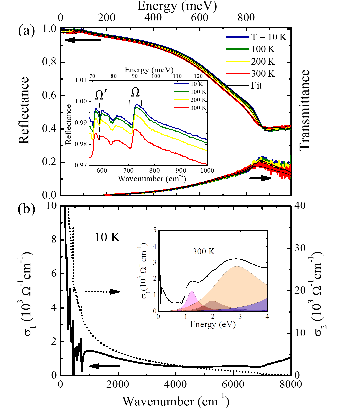
Results.—Fig. 1 (a) shows the reflectance and transmittance of the thin film for 0.1 eV. We fit and simultaneously using the multilayer (film+substrate) analysis algorithm of the Kramers-Kronig (KK) constrained RefFit program [25, 26]. The dielectric functions of the bare -substrate were characterized separately and fed into the analysis. Fig. 1 (b) displays and , the real and imaginary optical conductivity of , respectively, obtained from the fit at = 10 K. They consist of an intra-band (Drude) response in the low-energy range and inter-band transitions at high energy 0.8 eV. When compared to the previous optical study on a single crystal [20], the inter-band transitions of our film are almost identical, whereas the Drude peak is notably broader. The latter is attributed to additional scatterings of the carrier at the twin-boundary and the top / bottom surfaces of the film [21]. In the inset of Fig. 1 (a) we highlight that there is a distinct peak-like feature at = 90 meV in . We label it conveniently as Peak- and will revisit it frequently later for data analysis. To add, refers to a dip at a lower energy.

In Fig. 2 we show the scattering rate and effective mass of the Drude carrier. They are calculated from the Drude and using the extended Drude analysis formula
| (1) |
| (2) |
The increases markedly for and drops from the same frequency. At = 90 meV, there is a dispersive structure in and that triggers the frequency-dependent changes. This structure originates from the Peak- in . The frequency-dependent and are the characteristic behavior of an electron-boson interaction: For a conducting material with an electron-boson interaction, increases as exceeds the boson energy, and simultaneously, begins to decrease from a dressed mass ( 1) to bare band mass (= 1) [27, 28, 29, 30, 31, 32]. Fig. 2 shows that an electron-boson coupling is occurring in with a boson mode located at = .
To ensure that the frequency-dependent and are intrinsic properties of , we synthesized a pure Pd-thin film (thickness = 15 nm) using MBE on the same substrate () and performed the same optical measurements (R and T) and extended-Drude analysis. The Pd-film is classified as a noble metal such as Au or Ag films. In contrast to , and of the Pd-film are independent of frequency as expected for a simple Drude metal. (See Supplementary Fig. S1) This comparative study supports that and in Fig. 2 are not artifacts caused by, for example, the substrate but are the genuine properties of . In addition, the Pd-film does not show Peak- (and ) in R() indicating that Peak- (and ) is intrinsic to as well. (See Supplementary Fig. S2). In Fig. 2, and become considerably noisy for the range . The unwanted noises are caused mostly by the strong optical phonons of , which we present in detail in Supplementary Fig. S2. Ideally, the substrate phonons should be isolated from the thin film during the data analysis (fitting). However, in practice, they are not perfectly removed, causing the noise. Importantly, Fig. S2 demonstrates that, unambiguously, Peak- arises not from the substrate but from . Given that Peak- is driving the frequency-dependent and , it is crucial to unveil the origin of Peak- in order to understand the electron-boson interaction of .
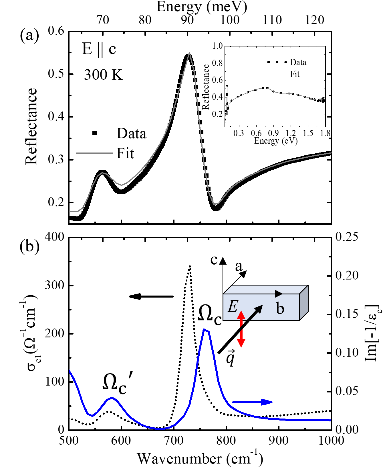
In Fig. 3 (a) we measured the c-axis reflectance of the single crystal. To measure ,
a focused IR beam from a microscopic FTIR polarized along the c-axis ( c) was illuminated on the side facet of the d 100 m-thick single crystal. In this manner, reproducible data were obtained for 500 cm-1.
The shows a prominent structure at = 90 meV and a minor one at 70 meV.
The wide-range (inset) reveals an insulating behavior of the c-axis, which contrasts sharply with the metallic of the ab-plane.
We fit the using the KK-constrained RefFit and calculated the complex c-axis optical conductivity and dielectric constant .
In the fit, we constrained to match the c-axis dc-conductivity at = 0 [33].
In Fig. 3 (b), we show the real part of . is peaked at = 730 cm-1 and 570 cm-1, which represents two transverse optical phonons (TO) of the c-axis. These c-TO phonons propagate along the ab-plane, q ab.
We also calculate the dielectric loss function Im[], which shows two peaks and representing the c-axis LO phonons. They propagate along q c. Note that, remarkably, is very close to Peak-, suggesting that it is a possible source of Peak-. The c-TO phonon (q ab), which is also close to Peak-, is not excited in the normal-incidence thin film measurements (q c) in Fig. 1, thus cannot create Peak-. As for , its energy is close to the dip of Fig. 1.
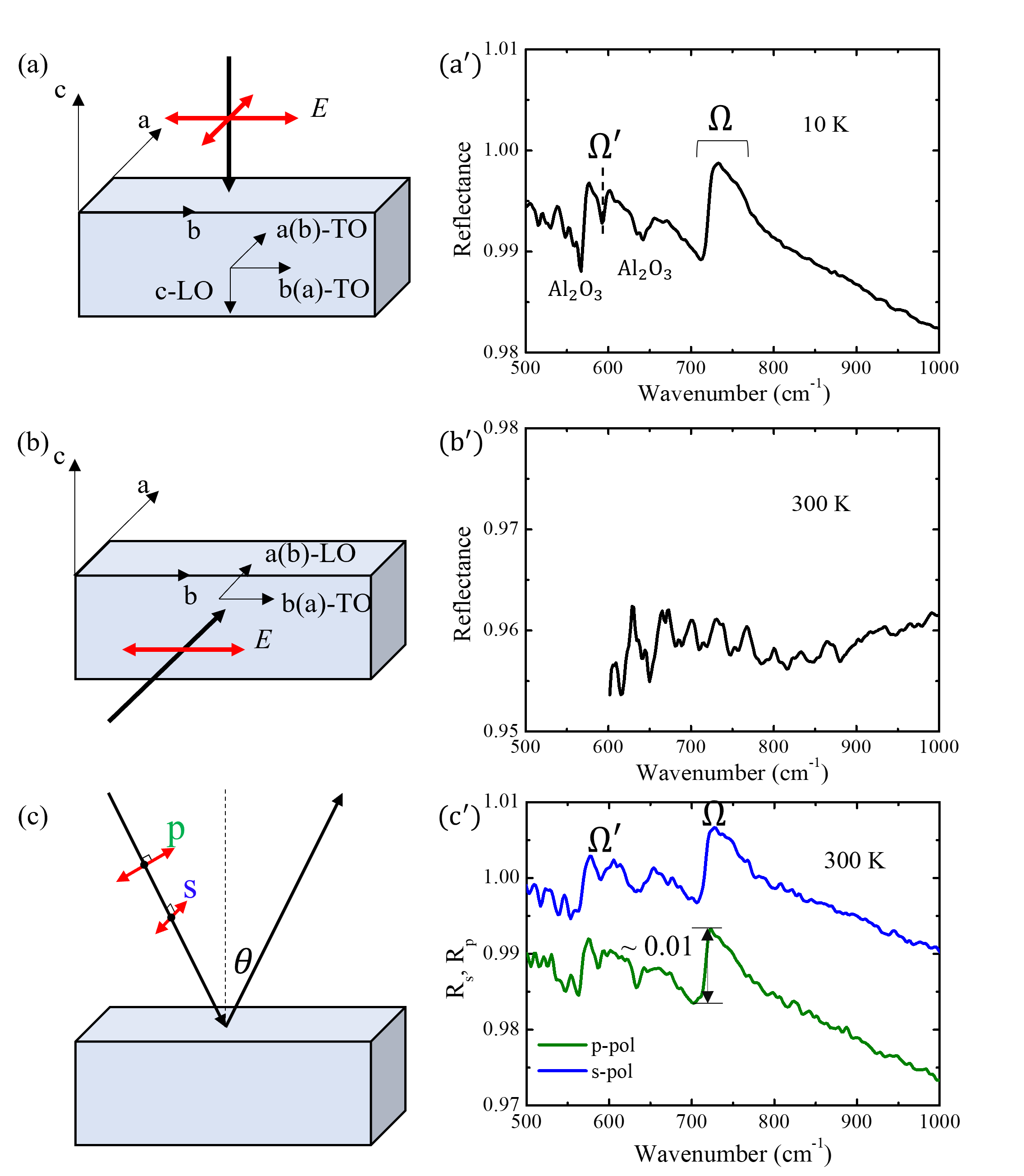
To confirm the presumption that Peak- originates from , we perform further polarized reflectance measurements. In Fig. 4 (a) incident light propagates along the c-axis while the electric field is parallel to the ab-plane. This optical configuration ( c, ab) can activate the ab-plane TO and the c-axis LO phonon. In Fig. 4 (b) we employed a different optical configuration a and b which activates the b-TO but not the c-LO. (To note, we use ’a’ and ’b’ to represent two orthogonal axes of the ab-plane but they do not indicate any specific crystallographic directions. The terms a-TO and b-TO are equivalent to ab-TO.) The R() in Fig. 4 (a′) and (b′) show that Peak- is activated in Fig. 4 (a), but is absent in Fig. 4 (b), demonstrating that ab-TO is excluded from the source of Peak-, thus leaving the c-LO () the only remaining candidate. The ab-TO phonons are another possible sources of Peak- but, according to Ref. [20], they are far from Peak-. In general, a c-axis optical phonon of a layered material does not appear in the ab-plane reflectivity due to forbidden symmetry. In , however, manifests itself in the ab-plane reflectivity as a result of coupling with the ab-plane Drude carrier. This coupling leads to the frequency-dependent and of Fig. 2.
In our near-normal ( = 10∘) reflectance measurement, incident light contains a small c
component, which may cause the c-axis phonons to leak into the ab-plane reflectivity. In this case, Peak- may appear in R() even if the electron-phonon coupling were absent.
To test if this is the case for Fig. 4 (a′), we measured R() using the s- and p-polarization as shown in Fig. 4 (c): In the s-polarization, the light has no c component, whereas the p-polarization does have a finite c component. The R() in Fig. 4 (c′) shows that Peak- is activated in the s-polarization with similar strength as in the p-polarization. This result rules out the leakage scenario of Peak-.
To reinforce our conclusion, we theoretically the calculated grazing-incidence R()
at incidence angles
= 10∘ and 20∘. For this, we used
the ab-plane and c-axis dielectric functions measured in Fig. 1 and Fig. 3, respectively.
The calculation results, shown in the Supplementary
Fig. S3, reveal that at = 20∘, the c-LO
leaks into the ab-plane reflectivity in the p-polarization, giving rise to a peak with 5 in height. However, this peak height is far weaker than the actual height of Peak- in Fig. 4 (c′), 0.01. Furthermore, at the experimental angle = 10∘,
the calculated leakage becomes even smaller, and the peak is too weak to be detected.
This observation supports again that the -field leakage cannot account for Peak- in . We thus conclude that the c-LO does couple with the ab-plane Drude carrier manifesting itself as Peak- in the ab-plane reflectance.
Discussion.—To compare with HTSC, they are the two types of rare materials that exhibit the coupling of the ab-plane carrier with c-LO phonons. One major difference, however, is that the Drude carrier couples in whereas it is the mid-IR band in HTSC [6]. Therefore, in the latter, c-LO does not influence the dc-transport. On the contrary, the c-LO of may play a significant role in the ab-plane transport such as the hydrodynamic charge flow. We emphasize that is the first layered material in which the c-LO couples with the ab-plane Drude carriers.
To discuss , we examine if it arises from like did from . For this, we compare the ab-plane with the c-axis Im[] in Fig. S4 following a similar approach as in Ref.[6]. The Peak- occurs at the same energy as but with a significantly narrower width. On the contrary, for the single crystal , an optical peak occurs in the ab-plane at the same energy and with similar width as , supporting that the electron-phonon interaction persists for [20]. In the thin film, is highly uncertain in the region of , hindering precise determination of the spectral shape. To definitely establish the correlation with , improved measurements that overcome the noise are needed. To further compare the thin film and single crystal results, we note that Peak- has an asymmetric, Fano-like shape in in both cases. However, they have the opposite Fano-asymmetry signs and different strengths of asymmetry (See Supplementary Fig. S4 and Ref. [20]). Such differences suggest that substantial thickness-dependent effects exist for the electron-phonon coupling. Lastly, while we focused primarily on electron-phonon coupling in this paper, our data may suggest that another type of interaction, such as the electron-electron interaction, may apply to as well. (See Supplementary Fig. S5)
Conclusion.—In conclusion, we performed polarized infrared transmission and reflection measurements on a thin film. In the ab-plane, the scattering rate and effective mass of the Drude carriers increased and decreased for , respectively, driven by Peak-. In the c-axis measurement on a single crystal, a longitudinal optical phonon was found at as evidenced by a peak of the loss function Im[]. Further optical measurements employing different (q, E) configurations revealed that Peak- is activated due to the interaction of the ab-plane Drude carriers with the c-LO phonon. This electron-phonon interaction leads to the frequency-dependent and . Our conclusion was established through the extensive supporting measurements on the pure Pd-film, bare substrate, and the s- and p-polarized grazing-incidence reflection calculations. The coupling of the ab-plane Drude electron with the c-LO phonon implies that c-LO may play a significant role in the characteristic ab-plane carrier dynamics of such as the ultra-high dc-conductivity, phonon-drag, and hydrodynamic charge flow, which is worthy for further studies. We want to remark that we were heavily assisted by Ref.[6] and Ref.[20] in conducting data analysis and interpretations.
Acknowledgement.—We thank C. C. Homes, D. Valentinis, J. Zaannen, D. Van Der Marel, Hyoung Joon Choi, and Han-Jin Noh for their helpful discussions. This work was supported by the NRF-2021R1A2C1009073 of Korea funded by the Ministry of Education. D. S was partially supported by MOLIT as Innovative Talent Education Program for Smart City. The work at Rutgers University is supported by National Science Foundation’s DMR2004125 and Army Research Office’s W911NF2010108. S.B.C. was supported by the NRF of Korea funded by MSIT (2020R1A2C1007554) and the Ministry of Education (2018R1A6A1A06024977). Research in Dresden benefits from the environment provided by the DFG Cluster of Excellence ct.qmat (EXC 2147, project ID 390858940). The work at HYU was supported by the National Research Foundation grant of Korea (NRF) funded by the Korean government (MSIT) (2022R1F1A1072865 and RS-2022-00143178) and BrainLink program funded by the Ministry of Science and ICT through the National Research Foundation of Korea (2022H1D3A3A01077468).
References
- Basov et al. [2011] D. N. Basov, R. D. Averitt, D. Van Der Marel, M. Dressel, and K. Haule, Reviews of Modern Physics 83, 471 (2011).
- Kamarás et al. [1990] K. Kamarás, S. Herr, C. Porter, N. Tache, D. Tanner, S. Etemad, T. Venkatesan, E. Chase, A. Inam, X. Wu, et al., Physical review letters 64, 84 (1990).
- Reedyk et al. [1988] M. Reedyk, D. Bonn, J. Garrett, J. Greedan, C. Stager, T. Timusk, K. Kamarás, and D. Tanner, Physical Review B 38, 11981 (1988).
- Reedyk et al. [1992] M. Reedyk, T. Timusk, J. Xue, and J. Greedan, Physical Review B 45, 7406 (1992).
- Foster et al. [1990] C. Foster, K. Voss, T. Hagler, D. Mihailović, A. Heeger, M. Eddy, W. Olson, and E. Smith, Solid state communications 76, 651 (1990).
- Reedyk and Timusk [1992] M. Reedyk and T. Timusk, Physical review letters 69, 2705 (1992).
- Higuchi et al. [1998] T. Higuchi, T. Tsukamoto, M. Tanaka, H. Ishii, K. Kanai, Y. Tezuka, S. Shin, and H. Takei, Journal of electron spectroscopy and related phenomena 92, 71 (1998).
- Seshadri et al. [1998] R. Seshadri, C. Felser, K. Thieme, and W. Tremel, Chemistry of materials 10, 2189 (1998).
- Hasegawa et al. [2001] M. Hasegawa, T. Higuchi, M. Tanaka, T. Tsukamoto, S. Shin, and H. Takei, Materials Transactions 42, 961 (2001).
- Eyert et al. [2008] V. Eyert, R. Frésard, and A. Maignan, Chemistry of Materials 20, 2370 (2008).
- Noh et al. [2009a] H.-J. Noh, J. Jeong, J. Jeong, E.-J. Cho, S. B. Kim, K. Kim, B. Min, and H.-D. Kim, Physical review letters 102, 256404 (2009a).
- Noh et al. [2009b] H.-J. Noh, J. Jeong, J. Jeong, H. Sung, K. J. Park, J.-Y. Kim, H.-D. Kim, S. B. Kim, K. Kim, and B. Min, Physical Review B 80, 073104 (2009b).
- Ong et al. [2010] K. P. Ong, J. Zhang, S. T. John, and P. Wu, Physical Review B 81, 115120 (2010).
- Mackenzie [2017] A. P. Mackenzie, Reports on Progress in Physics 80, 032501 (2017).
- Daou et al. [2017] R. Daou, R. Frésard, V. Eyert, S. Hébert, and A. Maignan, Science and Technology of Advanced Materials 18, 919 (2017).
- Harada [2021] T. Harada, Materials Today Advances 11, 100146 (2021).
- Hicks et al. [2012] C. W. Hicks, A. S. Gibbs, A. P. Mackenzie, H. Takatsu, Y. Maeno, and E. A. Yelland, Physical Review Letters 109, 116401 (2012).
- Lynch and Hunter [1997] D. W. Lynch and W. Hunter, in Handbook of optical constants of solids (Elsevier, 1997) pp. 275–367.
- Moll et al. [2016] P. J. Moll, P. Kushwaha, N. Nandi, B. Schmidt, and A. P. Mackenzie, Science 351, 1061 (2016).
- Homes et al. [2019] C. Homes, S. Khim, and A. P. Mackenzie, Physical Review B 99, 195127 (2019).
- Brahlek et al. [2019] M. Brahlek, G. Rimal, J. M. Ok, D. Mukherjee, A. R. Mazza, Q. Lu, H. N. Lee, T. Z. Ward, R. R. Unocic, G. Eres, et al., Physical Review Materials 3, 093401 (2019).
- Homes et al. [1993] C. C. Homes, M. Reedyk, D. Cradles, and T. Timusk, Applied optics 32, 2976 (1993).
- Shannon et al. [1971] R. D. Shannon, D. B. Rogers, and C. T. Prewitt, Inorganic Chemistry 10, 713 (1971).
- Takatsu et al. [2010] H. Takatsu, S. Yonezawa, S. Fujimoto, and Y. Maeno, Physical review letters 105, 137201 (2010).
- Kuzmenko [2005] A. Kuzmenko, Review of scientific instruments 76, 083108 (2005).
- Kuzmenko [2016] A. Kuzmenko, Reffit (2016).
- Carbotte [1990] J. Carbotte, Reviews of Modern Physics 62, 1027 (1990).
- Allen [1971] P. Allen, Physical Review B 3, 305 (1971).
- Shulga et al. [1991] S. Shulga, O. Dolgov, and E. Maksimov, Physica C: Superconductivity 178, 266 (1991).
- Stricker et al. [2014] D. Stricker, J. Mravlje, C. Berthod, R. Fittipaldi, A. Vecchione, A. Georges, and D. Van Der Marel, Physical review letters 113, 087404 (2014).
- Kostic et al. [1998] P. Kostic, Y. Okada, N. Collins, Z. Schlesinger, J. Reiner, L. Klein, A. Kapitulnik, T. Geballe, and M. Beasley, Physical Review Letters 81, 2498 (1998).
- Schlesinger et al. [1990] Z. Schlesinger, R. Collins, F. Holtzberg, C. Feild, S. Blanton, U. Welp, G. Crabtree, Y. Fang, and J. Liu, Physical review letters 65, 801 (1990).
- Putzke et al. [2020] C. Putzke, M. D. Bachmann, P. McGuinness, E. Zhakina, V. Sunko, M. Konczykowski, T. Oka, R. Moessner, A. Stern, M. König, et al., Science 368, 1234 (2020).