Intrinsic persistent spin helix in 2D T-XY (XY=P, As, Sb and Bi)
Abstract
The persistent spin helix (PSH) is robust against spin-independent scattering and renders an extremely long spin lifetime, which can improve the performance of potential spintronic devices. To achieve the PSH, a unidirectional spin configuration is required in the momentum space. Here, T-XY (XY=P, As, Sb and Bi) monolayers with dynamical, mechanical and thermal stabilities are predicted to intrinsically possess PSH. Due to the point-group symmetry, a unidirectional spin configuration is preserved in the out-of-plane direction for both conduction and valence bands around the high-symmetry point. That is, the expectation value of the spin only has the out-of-plane component . The application of an out-of-plane external electric field can induce in-plane components and , thus offering a promising platform for the on-off logical functionality of spin devices. Our work reveals a new family of T-phase two-dimensional (2D) materials, which could provide promising applications in spintronic devices.
I Introduction
In a material with broken inversion symmetry, the spin-orbital coupling (SOC) induces momentum ()-dependent spin-orbit field (SOF), which can lift spin degeneracy and leads to the nontrivial -dependent spin textures of the spin-split bands through Rashba and Dresselhaus effectsp1 ; p2 . Practically, the strong Rashba SOC allows for electrostatic manipulation of the spin states, which has potential application for non-charge-based computing and information processingp3 ; p4 ; p5 . However, strong SOC can cause spin decoherence, which leads to the reduced spin lifetime. The impurities and defects can change the momentum of electrons in a diffusive transport regime, and simultaneously randomize the spin due to the -dependent SOF, which induces spin decoherence through the Dyakonov-Perel (DP) mechanism and limits the performance of potential spintronic devicesp6 .
To overcome spin dephasing, a possible way is designing a structure with the SOF orientation to be unidirectional, which can preserve a unidirectional spin configuration in the space. The unidirectional SOF will lead to a spatially periodic mode of the spin polarization, which is known as the persistent spin helix (PSH)p7 ; p8 . The spin dephasing can be suppressed by PSH due to SU(2) spin rotation symmetry, which renders an extremely long spin lifetimep7 ; p9 . The PSH has been demonstrated on various quantum well (QW) heterostructures, interface and surfacep10 ; p11 ; p12 ; p13 ; p13-1 ; p14 ; p15 . Recently, a different approach for achieving the PSH is imposing the specific symmetry of the crystal, which has been realized in bulk-, layered- and two-dimensional (2D)-ferroelectric systemsp16 ; p17 ; p18 ; p19 ; p20 ; p21 ; p22 ; p23 ; p24 ; p25 ; p26 . However, the search for 2D materials with intrinsic PSH has lately been very demanding of attention due to their potential for miniaturization spintronic devices.
Recently, similar to the -phase, the T-phase MZ (M=Sn and Ge; Z=S and Se) has been proposed with excellent thermal, dynamical and mechanical stabilities, which exhibits symmetry and fold characteristics similar to ”triple-staggered layers”apl . These T-MX monolayers possess fine piezoelectric performance and stabilityapl . Here, the T-XY (XY=P, As, Sb and Bi) monolayers are proposed with dynamical, mechanical and thermal stabilities, which possess the same number of valence electrons with MX (M=Sn and Ge; X=S and Se). The T-XY are predicted to intrinsically possess PSH with a unidirectional out-of-plane spin configuration () for both conduction and valence bands due to the point-group symmetry. When an out-of-plane external electric field is applied, the in-plane components and can be induced, which offers a promising platform for the on-off logical functionality of spin devices.
The rest of the paper is organized as follows. In the next section, we shall give our computational details and methods. In the next few sections, we shall present crystal structure and stability, electronic structures and PSH of T-XY (XY=P, As, Sb and Bi) monolayers. Finally, we shall give our discussion and conclusion.
II Computational detail
Within density functional theory (DFT)1 , the first-principle calculations are carried out by using the projector augmented wave (PAW) method as implemented in Vienna ab initio Simulation Package (VASP)pv1 ; pv2 ; pv3 . We use the generalized gradient approximation of Perdew, Burke and Ernzerhof (GGA-PBE)pbe as exchange-correlation functional. The SOC is included to investigate electronic structures and PSH of T-XY (XY=P, As, Sb and Bi), and the details of the SOC implementation in the PAW methodology are given in ref.soc . The energy cut-off of 500 eV, total energy convergence criterion of eV and force convergence criteria of 0.001 are set to perform the first-principles calculations. A vacuum space of more than 28 between slabs along the direction is added to eliminate the spurious interactions. A 351 supercell is used to calculate the phonon spectrum within the finite displacement method by using the Phonopy codepv5 . The elastic stiffness () are obtained by strain-stress relationship (SSR), and the 2D have been renormalized by =, where is the length of unit cell along direction. The constant energy contour plots of the spin texture are calculated by the PYPROCAR codepy . A 9181 k-point meshes in the first Brillouin zone (BZ) are adopted for all calculations.
| Name | ||||||||||
| 9.38 | 3.48 | 9.87 | 10.72 | 77.64 | 18.97 | 8.39 | 66.00 | 1.050 | 1.047 | |
| 9.66 | 3.94 | 7.12 | 11.02 | 55.07 | 13.33 | 4.92 | 38.01 | 0.307 | 0.289 | |
| 8.95 | 3.83 | 3.50 | 9.19 | 60.04 | 17.71 | 2.09 | 35.91 | 0.366 | 0.332 | |
| 8.40 | 4.00 | 4.83 | 3.34 | 54.15 | 17.10 | 4.62 | 51.84 | 0.621 | 0.381 | |
| 9.45 | 4.10 | 7.99 | 9.49 | 49.51 | 12.19 | 6.17 | 38.24 | 0.319 | 0.108 | |
| 9.94 | 4.35 | 7.49 | 9.94 | 43.04 | 10.64 | 5.19 | 29.85 | 0.354 | 0.026 |
III Crystal structure and stability
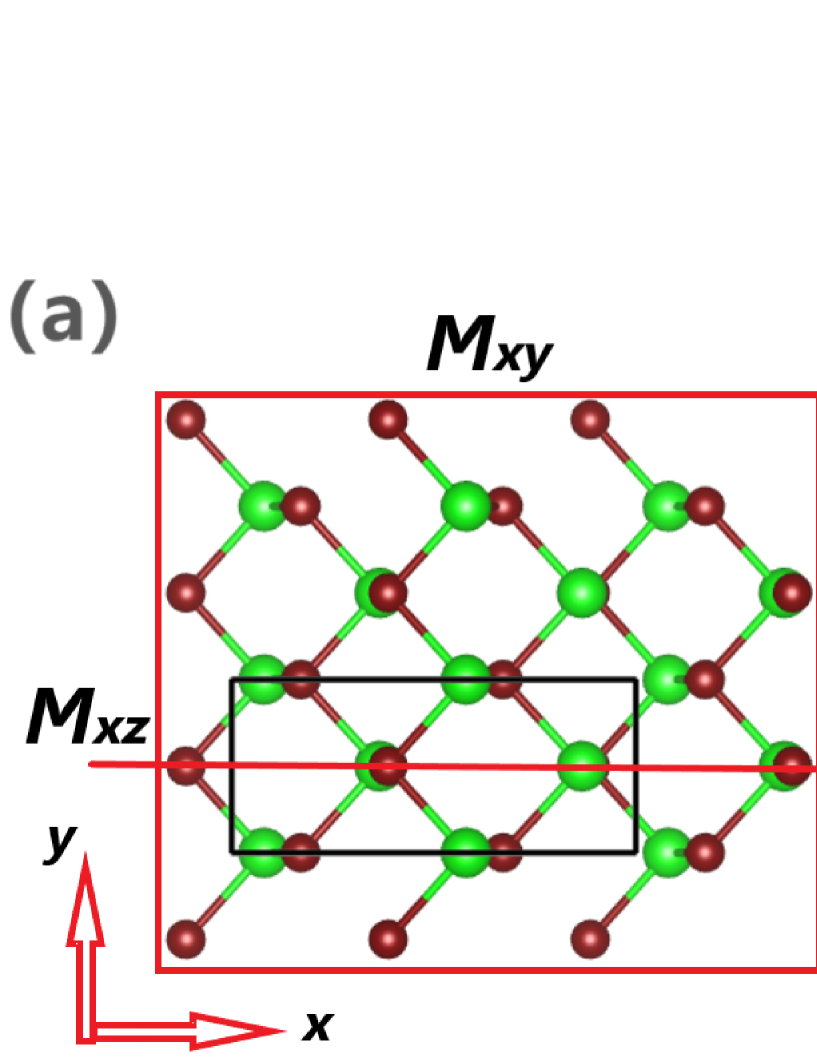
The top and side views of crystal structures of T-XY (XY=P, As, Sb and Bi) are shown in Figure 1 (a) and (b). The primitive cell contains eight atoms, including four X atoms and four Y atoms, and each X (Y) atom is connected to three surrounding Y (X) atoms. Their optimized lattice parameters and along the and directions are listed in Table 1.
The T-phase has four symmetry operations: (i) identity operation ; (ii) twofold screw rotation ; (iii) glide reflection ; and (iv) reflection with respect to the plane. The is performed by twofold rotation around the x axis (), followed by translation of =(/2, /2). The can be obtained by reflection with respect to the plane followed by translation . The T-phase lacks inversion symmetry, allowing piezoelectric response. Because these T-XY monolayers share similar behavior, in the following, we shall mainly focus on T-SbP monolayer as a representative. The results of the remaining five monolayers are briefly mentioned or put in FIG.1, FIG.2, FIG.3, FIG.4, FIG.5, FIG.6 and FIG.7bc .
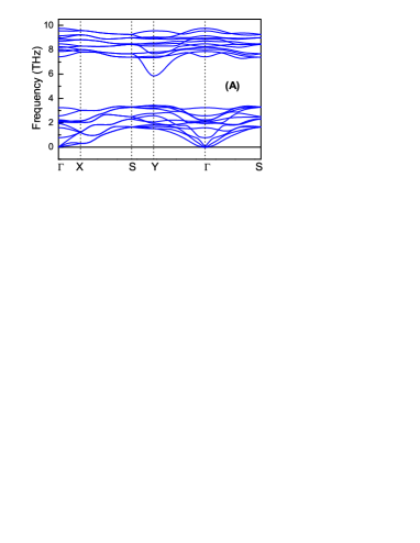
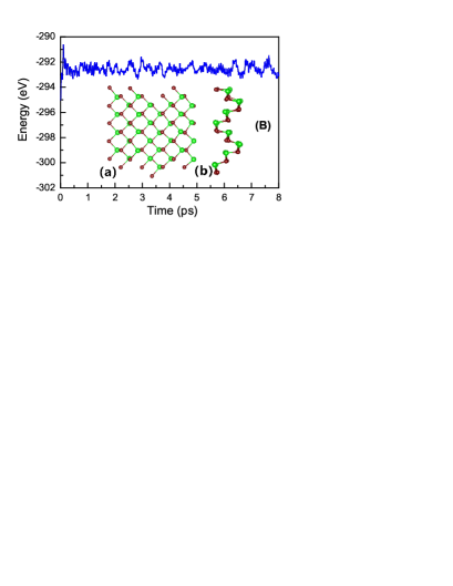
To verify their dynamical stabilities, their phonon dispersions are calculated. Figure 2 (A) plots the result for monolayer SbP, which shows no imaginary frequency, indicating that the structure is dynamically stable. To investigate the thermal stability, the ab-initio molecular dynamics (AIMD) simulations are performed with a 241 supercell and a time step of 1 fs. Figure 2 (B) shows the simulation result on monolayer T-SbP at 300 K for 8 ps. One observes that the energy fluctuates within a small range during the whole simulation time, and the overall structure is well maintained at this temperature, indicating its good thermal stability. The linear elastic constants are calculated to determine their mechanical stabilities. Due to symmetry, four independent elastic constants (, , and ) can be observed, which are listed in Table 1. These meet Born-Huang criteria of mechanical stability (, and )ela , thereby verifying their mechanical stabilities. The direction-dependent Young’s modulus can be obtained asela1 :
| (1) |
where is the polar angle measured from , and . According to FIG.8 and FIG.9bc , obvious anisotropy of elasticity is observed in these T-XY monolayers. The Young’s modulus of T-XY along and directions are listed Table 1. It is clearly seen that is very smaller than . This indicates that the T-XY is more flexible and deformable along direction, which plays a positive effect on their piezoelectricityapl .
Although these T-XY monolayers have not been experimentally synthesized, the above calculated results show that they possess good thermal stability as well as positive dynamical and mechanical stabilities. Therefore, we expect that these monolayers can be synthesized experimentally in the future.
IV electronic structures and persistent spin helix
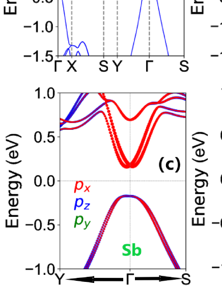
Figure 3 shows the energy band structures of T-SbP calculated along high-symmetry paths, and those of the other five are plotted in FIG.3, FIG.4, FIG.5, FIG.6 and FIG.7bc . Without including the SOC, the T-SbP, T-BiP, T-BiAs and T-BiSb are indirect bandgap semiconductors, and the conduction band bottom (CBM) locates at point, while the valence band maximum (VBM) slightly deviates from along the -Y path. However, the T-AsP and T-SbAs are direct bandgap semiconductors with both CBM and VBM at point. The gaps of T-AsP, T-SbP, T-SbAs, T-BiP, T-BiAs and T-BiSb are 1.050 eV, 0.366 eV, 0.307 eV, 0.621 eV, 0.319 eV and 0.354 eV, respectively. When including the SOC, the energy band structures of T-XY are modified, and they all become indirect bandgap semiconductors with both CBM and VBM slightly deviating from point. The GGA+SOC gaps of six monolayers are reduced with respect to GGA ones. For T-XY (XY=P, As and Sb), the changes of gap are small, while the gaps of T-BiY (Y=P, As and Sb) vary greatly. The gaps of T-AsP, T-SbP, T-SbAs, T-BiP, T-BiAs and T-BiSb become 1.047 eV, 0.332 eV, 0.289 eV, 0.381 eV, 0.108 eV and 0.026 eV, respectively. The related gap data are summarized in Table 1. Importantly, a sizable splitting of the bands produced by the SOC is observed. This splitting is especially pronounced around the point near both the VBM and CBM. According to Figure 3 (c) and (d), the Sb- and P- orbitals contribute dominantly to the CBM, while the VBM are mainly from the contributions of the Sb- and P- orbitals.
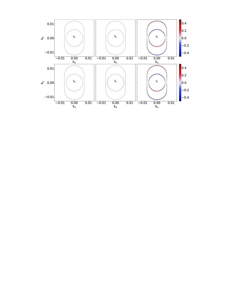
For T-SbP monolayer, the top planes of Figure 4 and Figure 5 show the spin textures of conduction and valence bands calculated in a plane centered at the point with the isoenergetic surface of 0.25 eV and -0.25 eV, respectively. It is clearly seen that the spin polarization is originated from the out-of-plane component , while the in-plane components of spin ( and ) are zero. This means that the spin texture is unidirectional, which is very different from the in-plane Rashba spin textures. Such a spin texture produces a unidirectional out-of-plane SOF, resulting in a persistent spin texture (PST). The unidirectional SOF is robust against spin-independent scattering due to the PSH state, which leads to an extremely long spin lifetime by suppressing the DP spin-relaxation mechanismp6 .
To explain the PST with only out-of-plane component , we establish an effective Hamiltonian expanded at point. The twofold degeneracy at corresponds to the double-valued irreducible representation of . Taking the two states as basis, the generators, and , are represented in the matrix form as
| (2) |
is time reversal symmetry operation. These symmetries constrain the Hamiltonian by
| (3) |
Expanding to order, the Hamiltonian can be written as:
| (4) |
where is 22 identity matrix, is the Pauli matrices, ( and ) is the wave vector, and are model parameters. Since the spin operator commutes with the Hamiltonian Equation 4, the spin operator is a conserved quantity. The expectation value of the spin only has the out-of-plane component, which produces the unidirectional out-of-plane spin configuration in space.
On the other hand, by ignoring the high-order items, the linear-term parameter , through the relation , can be obtained, where and are the shifting energy and the wave vector along the direction. The formation of the PSH mode should have a substantially small wavelength of the spin polarization. Here, the wavelength can be estimated by using , where is the electron effective mass (Here, we only consider the conduction bands due to large spin-splitting.). The is evaluated from the band dispersion along the -Y line in the CBM. For several selected 2D PSH systems, the spin-splitting parameter , effective mass , and the wavelength of the spin polarization are summarized in Table 2. These of T-SbP, T-BiP, T-BiAs and T-BiSb are comparable with those reported for several 2D PSH systems, and the small wavelength of the PSH mode is typically on the scale of the lithographic dimension used in the recent semiconductor industry. Thus, the T-SbP, T-BiP, T-BiAs and T-BiSb should be promising for miniaturization of spintronic devices.
| Monolayer | Reference | |||
| AsP | 0.059 | 0.120 | 67.675 | This work |
| SbAs | 0.454 | 0.092 | 11.471 | This work |
| SbP | 1.103 | 0.116 | 3.745 | This work |
| BiP | 2.454 | 0.094 | 2.077 | This work |
| BiAs | 4.359 | 0.067 | 1.640 | This work |
| BiSb | 7.113 | 0.056 | 1.203 | This work |
| MN | 0.071.67 | - | 1.82890 | Ref.p24 |
| GaMN | 0.532.65 | - | 1.206.57 | Ref.p20 |
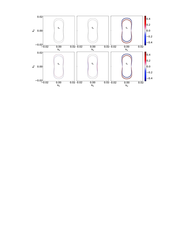
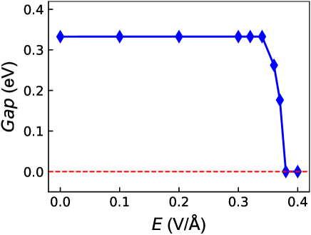
The application of the external electric field can modify the spin texture of T-SbP. So, an external out-of-plane electric field is applied, which breaks both the rotational and in-plane mirror symmetries. The gap of T-SbP as a function of is plotted in Figure 6, and the related energy band structures are shown in FIG.10bc . It is clearly seen that the gap basically remains unchanged, when is less than about 0.34 . At about =0.38 , a semiconductor-to-metal phase transition can be observed.
Under the out-of-plane external electric field, the effective Rashba contribution should be added in Hamiltonian Equation 4, which has the isotropic formp1 :
| (5) |
The introducing Rashba term will induce the in-plane spin components due to the broken in-plane mirror symmetry caused by the out-of-plane external electric field. To confirm this, the bottom planes of Figure 4 and Figure 5 show the spin textures of conduction and valence bands calculated in a plane centered at the point with the isoenergetic surface of 0.25 eV and -0.25 eV for T-SbP at =0.30 . It is clearly observed that significant in-plane spin components ( and ) are induced, thus breaking the PST and perturbing the PSH state.
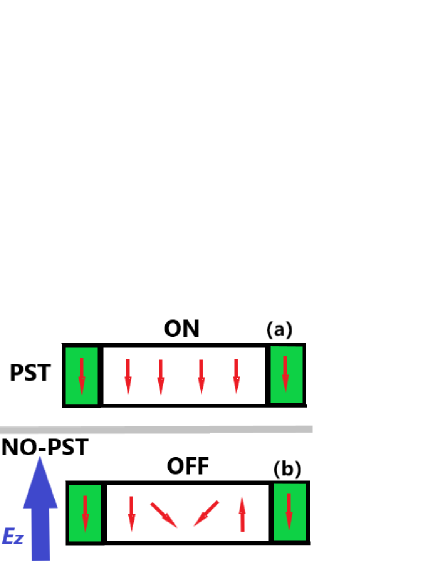
The in-plane spin components can be turned on by applied out-of-plane electric field, which provides a possibility of the on-off logical functionality of spin devices by controlling the passage of electrons (see Figure 7). For example, two ferromagnetic (FM) electrodes in the same direction are set for source and drain electrodes. Without the out-of-plane electric field, the out-of-plane orientation of the spin polarization injected from the source electrode maintains due to PST, when the injected electrons pass through the T-SbP channel (Figure 7 (a)). When the external electric field is applied, the PST is broken, and the PSH state is perturbed. The spin of electrons in the channel will rotate, and will be blocked by the drain electrode (Figure 7 (b)). The function of spintronic switch can be realized in the possible spintronic device.
V Discussion and Conclusion
A general form of the SOC Hamiltonian in solid-state materials can be expressed asq7-9 ; q7-10 :
| (6) |
where is the strength of the SOC, and =(, , ) are the Pauli matrices. For T-SbP, the spontaneous in-plane electric polarization is oriented along direction. The Equation 6 is written as:
| (7) |
This is consistent with Equation 4, when ignoring the higher order terms of .
The electric field along direction can also be induced with a uniaxial in-plane strain by piezoelectric effect, and then tune spin-splitting of T-SbP. When a uniaxial in-plane vibration is applied to T-SbP, the spin-splitting will be modulated periodically. As shown in FIG.11 (a)bc , the compressive strain produces negative electric field, and then reduces spin-splitting of PST. However, FIG.11 (b)bc shows that the tensile strain induces positive electric field, and then enhances spin-splitting of PST. So, the orthorhombic primitive cell is used to calculate the piezoelectric stress coefficients of T-XY (XY=P, As, Sb and Bi), and then the piezoelectric strain coefficients are obtained by the and apl . The related data are listed in TABLE Ibc . The of T-SbP is as high as 266.15 pm/V, which plays a positive effect on tuning spin-splitting by piezoelectric effect. Piezotronic effect on Rashba SOC in a ZnO/P3HT nanowire array structure has been investigated experimentallyydt . It is found that the Rashba SOC can be effectively tuned by inner-crystal piezo-potential created inside the ZnO nanowires instead of an externally applied voltage. So, the spin-splitting of PST in T-XY (XY=P, As, Sb and Bi) can be tuned by piezoelectric effect.
In summary, based on the first-principles calculations along with symmetry analysis, we have systematically investigated the electronic properties of 2D T-XY (XY=P, As and Sb) with dynamical, mechanical and thermal stabilities. Because of point-group symmetry, the unidirectional out-of-plane spin configurations are preserved in 2D T-XY (XY=P, As and Sb), giving rise to the PSH state. It is found that this PSH is observed near both VBM and CBM around point. The out-of-plane electric field can be used to perturb PSH, which provides possibility to realize electronic device of switching function. Our works reveal a new 2D family of materials that have great potential for spintronic device applications.
Acknowledgements.
This work was supported by Natural Science Basis Research Plan in Shaanxi Province of China (No. 2021JM-456). We are grateful to Shanxi Supercomputing Center of China, and the calculations were performed on TianHe-2.References
- (1) E. I. Rashba, Sov. Phys. Solid State 2, 1224 (1960).
- (2) G. Dresselhaus, Phys. Rev. 100, 580 (1955).
- (3) J. Nitta, T. Akazaki, H. Takayanagi, and T. Enoki, Phys. Rev. Lett. 78, 1335 (1997).
- (4) A. Manchon, H. C. Koo, J. Nitta, S. M. Frolov, and R. A. Duine, Nat. Mater. 14, 871 (2015).
- (5) P. Chuang, S. H. Ho, L. W. Smith et al., Nat. Nanotechnol. 10, 35 (2009).
- (6) M. I. Dyakonov and V. I. Perel, Sov. Phys. Solid State 13, 3023 (1972).
- (7) B. A. Bernevig, J. Orenstein, and S.-C. Zhang, Phys. Rev. Lett. 97, 236601 (2006).
- (8) J. Schliemann, Rev. Mod. Phys. 89, 011001 (2017).
- (9) P. Altmann, M. P. Walser, C. Reichl, W. Wegscheider, and G. Salis, Phys. Rev. B 90, 201306(R) (2014).
- (10) J. D. Koralek, C. P. Weber, J. Orenstein, B. A. Bernevig, S.-C. Zhang, S. Mack, and D. D. Awschalom, Nature (London) 458, 610 (2009).
- (11) M. P. Walser, C. Reichl, W. Wegscheider, and G. Salis, Nat. Phys. 8, 757 (2012).
- (12) J. Ishihara, Y. Ohno, and H. Ohno, Appl. Phys. Express 7, 013001 (2014).
- (13) M. Kohda, V. Lechner, Y. Kunihashi et al., Phys. Rev. B 86, 081306(R) (2012).
- (14) A. Sasaki, S. Nonaka, Y. Kunihashi, M. Kohda, T. Bauernfeind, T. Dollinger, K. Richter, and J. Nitta, Nat. Nanotechnol. 9, 703 (2014).
- (15) N. Yamaguchi and F. Ishii, Appl. Phys. Express 10, 123003 (2017).
- (16) M. A. U. Absor, F. Ishii, H. Kotaka, and M. Saito, Appl. Phys. Express 8, 073006 (2015).
- (17) L. L. Tao and E. Y. Tsymbal, Nat. Commun. 9, 2763 (2018).
- (18) C. Autieri, P. Barone, J. Slawiska and S. Picozzi, Phys. Rev. Materials 3, 084416 (2019).
- (19) H. Djani, A. C. Garcia-Castro, W. Y. Tong, P. Barone, E. Bousquet, S. Picozzi and P. Ghosez, npj Quant. Mater. 4, 51 (2019).
- (20) H. Ai, X. Ma, X. Shao, W. Li and M. Zhao, Phys. Rev. Materials 3, 054407 (2019).
- (21) S. A. Sasmito, M. Anshory, I. Jihad and M. A. U. Absor, Phys. Rev. B 104, 115145 (2021).
- (22) M. A. U. Absor and F. Ishii, Phys. Rev. B 103, 045119 (2021).
- (23) F. Jia, S. Hu, S. Xu, H. Gao, G. Zhao, P. Barone, A. Stroppa and W. Ren, J. Phys. Chem. Lett. 11, 5177 (2020).
- (24) M. A. U. Absor and F. Ishii, Phys. Rev. B 99, 075136 (2019).
- (25) M. A. U. Absor and F. Ishii, Phys. Rev. B 100, 115104 (2019).
- (26) H. Lee, J. Im and H. Jin, Appl. Phys. Lett. 116, 022411 (2020).
- (27) H. J. Zhao, H. Nakamura, R. Arras, C. Paillard, P. Chen, J. Gosteau, X. Li, Y. Yang and L. Bellaiche, Phys. Rev. Lett. 125, 216405 (2020).
- (28) H. Lei, T. Ouyang, C. Y. He, J. Li and C. Tang, Appl. Phys. Lett. 122, 062903 (2023).
- (29) P. Hohenberg and W. Kohn, Phys. Rev. 136, B864 (1964); W. Kohn and L. J. Sham, Phys. Rev. 140, A1133 (1965).
- (30) G. Kresse, J. Non-Cryst. Solids 193, 222 (1995).
- (31) G. Kresse and J. Furthmller, Comput. Mater. Sci. 6, 15 (1996).
- (32) G. Kresse and D. Joubert, Phys. Rev. B 59, 1758 (1999).
- (33) J. P. Perdew, K. Burke and M. Ernzerhof, Phys. Rev. Lett. 77, 3865 (1996).
- (34) S. Steiner, S. Khmelevskyi, M. Marsmann and G. Kresse, Phys. Rev. B 93, 224425 (2016).
- (35) A. Togo, F. Oba, and I. Tanaka, Phys. Rev. B 78, 134106 (2008).
- (36) U. Herath, P. Tavadze, X. He, E. Bousquet, S. Singh, F. Munoz and A. H. Romero, Comput. Phys. Commun. 251, 107080 (2020).
- (37) See Supplemental Material at [] for the phonon band dispersions, AIMD results and energy band structures of T-AsP, T-SbAs, T-BiP, T-BiAs and T-BiSb; the direction-dependent Young’s modulus and piezoelectric coefficients / of T-XY (XY=P, As, Sb and Bi); the energy band structures of T-SbP as a function of electric field ; schematic of strain-tuned persistent spin-splitting.
- (38) M. Born and K. Huang, Am. J. Phys. 23, 474 (1995).
- (39) E. Cadelano, P. L. Palla, S. Giordano and L. Colombo, Phys. Rev. B 82, 235414 (2010).
- (40) J. Nitta, T. Akazaki, H. Takayanagi and T. Enoki, Phys. Rev. Lett. 78, 1335 (1997).
- (41) A. Manchon, H. C. Koo, J. Nitta, S. M. Frolov and R. A. Duine, Nat. Mater. 14, 871 (2015).
- (42) L. Zhu, Y. Zhang, P. Lin et al., ACS Nano 12, 1811 (2018).