CamJ: Enabling System-Level Energy Modeling and Architectural Exploration for In-Sensor Visual Computing
Abstract.
CMOS Image Sensors (CIS) are fundamental to emerging visual computing applications. While conventional CIS are purely imaging devices for capturing images, increasingly CIS integrate processing capabilities such as Deep Neural Network (DNN). Computational CIS expand the architecture design space, but to date no comprehensive energy model exists. This paper proposes CamJ, a detailed energy modeling framework that provides a component-level energy breakdown for computational CIS and is validated against nine recent CIS chips. We use CamJ to demonstrate three use-cases that explore architectural trade-offs including computing in vs. off CIS, 2D vs. 3D-stacked CIS design, and analog vs. digital processing inside CIS. The code of CamJ is available at: https://github.com/horizon-research/CamJ.
1. Introduction
Visual computing applications on the horizon such as autonomous machines, computational photography, and space exploration all fundamentally rely on image sensing. While conventional CMOS Image Sensors (CIS) are responsible only for “imaging”, i.e., capturing pixels, CIS increasingly integrate computation capabilities, ranging from signal preprocessing (Cheng et al., 2008) to Deep Neural Networks (DNN) (Bong et al., 2017b; Hirata et al., 2021) and spanning both the analog and digital domain. For instance, a Nikon CIS (Hirata et al., 2021) integrates an image processor for per-tile exposure control; the Sony IMX 500 CIS (Eki et al., 2021) integrates a DNN accelerator with the pixel array for edge visual processing.
Computational CIS expand the traditional design space for architects and provide an exciting playground for exploring a diverse range of trade-offs. For instance, in-CIS processing consumes large volumes of pixel data in-situ and reduces the data transmission overhead; computing inside a sensor, however, is inefficient because CIS tend to be fabricated using older process nodes compared to standard CMOS nodes (limited by the photon sensing sensitivity (Theuwissen, 2021)), which offsets the gains from reducing the communication cost. Designers also face a myriad of choices when designing the in-sensor architecture. For instance, while 3D stacking improves energy efficiency by allowing for hybrid process integration (Xie and Zhao, 2015), it could also increase the power density and, thus, thermal-induced noise, requiring more processing downstream.
This paper presents CamJ, a first-of-its-kind energy modeling framework that empowers designers to navigate the large algorithm-hardware co-design space. CamJ provides a component-level energy estimation under a frame-per-second (FPS) target. To that end, CamJ models the interplay across main structures of a computational CIS pipeline: pixel sensing analog processing digital processing. Thus, CamJ enables end-to-end optimizations of the CIS architecture from photon ingestion to semantic results.
Design.
As an energy modeling tool for system-level exploration, CamJ has two design principles (Sec. 3). First, we use a declarative interface to describe the algorithm and hardware configurations. This is based on the observation that image processing algorithms have regular compute and memory access patterns; thus, a declarative description of the software and hardware is sufficient for accurate estimation of hardware access counts while simplifying users’ effort. The interface also decouples algorithm and hardware descriptions to facilitate iterative architectural explorations.
Second, we adapt the energy modeling methodology to account for the characteristics of the analog and digital domains (Sec. 4). In the digital domain, CamJ directly asks users for the per-operation energy of a Processing Element (PE) and per-access memory energy. Tools (Balasubramonian et al., 2017; Mittal et al., 2017) and data (Gao et al., 2017; Han et al., 2016) are widely available to obtain these statistics, which are routinely used in today’s digital accelerator simulation (Akhlaghi et al., 2018; Gao et al., 2017; Han et al., 2016; Feng et al., 2019). The energy of analog components, however, depends on many low-level circuit details (e.g., bias current, capacitance) that designers might not (need to) have access to, and no mature tools exist. Thus, CamJ provides default energy models for common analog components based on designs in classic CIS (Hsu et al., 2020; Park et al., 2021; Kaur et al., 2020; Young et al., 2019; Yang et al., 2015), while exposing an interface to accept custom designs from expert users.
Validation.
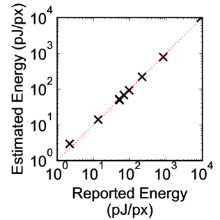
We perform extensive validation of CamJ against nine recent CIS chips (Sec. 5), which cover a diverse range of process nodes, pixel types, memory sizes, and forms of processing (e.g., analog vs. digital and pixel parallel vs. column parallel). Compared to the measured absolute energy consumption of the chips that span several orders of magnitude, CamJ achieves a Pearson Correlation Coefficient of 0.9999 and a Mean Absolute Percentage Error of 7.5%.
Use-cases.
We use three use-cases to demonstrate the architectural explorations that CamJ enables (Sec. 6). First, we show that a conventional 2D CIS design offers little energy benefit for computation-dominated algorithms. Second, moving toward a 3D design reduces energy due to the ability to use advanced process nodes for computation—at a cost of increasing power density. Third, analog processing in CIS could significantly reduce memory energy even when the compute energy reduction is modest.
In summary, this paper makes the following contributions:
-
•
We provide a comprehensive survey of the design and scaling trends of CIS, pointing out new opportunities for architectural exploration.
-
•
We propose the first component-level energy modeling tool for CIS and validate it against real silicon.
-
•
We use CamJ to show three use-cases, demonstrating architectural trade-offs of inside-vs-off CIS, 2D-vs-3D, and analog-vs-digital processing.
2. Motivation: Computational CIS Design and Scaling Trends
We first discuss the main design trend of CIS that underlies this paper: CIS are becoming increasingly computational (Sec. 2.1). We then explain the energy benefits of such computational CIS, a main driving force behind this design trend (Sec. 2.2). Finally, we discuss the challenges of reaping the energy benefits, which motivates this work (Sec. 2.3).
2.1. Design Trends
CIS Primer.
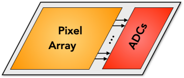
Fundamentally, a CIS consists of two basic components as illustrated in Fig. 2a: a light-sensitive photodiode array that converts photons to charges and a read-out circuit that converts charges to digital values (i.e., raw pixels) through the analog-to-digital converters (ADC). Traditionally, raw pixels are transferred to the host, e.g., a Systems-on-a-Chip (SoC) on a smartphone, through the MIPI CSI-2 interface (Group, 2021). The Image Signal Processor (ISP) in the SoC removes sensing artifacts (e.g., denoising) and prepares pixels for computer vision tasks and/or for visual display.
CIS Design Trend.
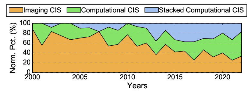
A clear trend in CIS design is to move into the sensor computations that are traditionally carried out outside the sensor, which gives rise to the notion of Computational CIS. Fig. 1 shows the percentage of computational CIS papers in ISSCC and IEDM from Year 2000 and Year 2022 with respect to all the CIS papers during the same time range. Increasingly more CIS designs integrate compute capabilities.
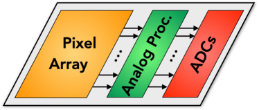
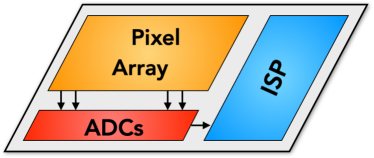
The computations inside a CIS could take place in both the analog and the digital domain. Fig. 2b illustrates one example where analog computing is integrated into a CIS chip. Analog operations usually implement primitives for feature extraction (Bong et al., 2017b, a), object detection (Young et al., 2019), and DNN inference (Hsu et al., 2020; Xu et al., 2021). Fig. 2c illustrates another example that integrates digital processing, such as ISP (Murakami et al., 2022), image filtering (Kim et al., 2005) and DNN (Bong et al., 2017a).
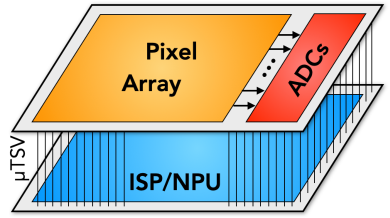
As the processing capabilities become more complex, CIS design has embraced 3D stacking technologies, as is evident by the increasing number of stacked CIS in Fig. 1. Fig. 2d illustrates a typical stacked design, where the processing logic is separated from, and stacked with, the pixel array layer. The different layers communicate through hybrid bond or micro Through-Silicon Via (TSV) (Liu et al., 2022; Tsugawa et al., 2017). The processing layer typically integrates digital processors; such as ISP (Kwon et al., 2020), image processing (Hirata et al., 2021; Kumagai et al., 2018), and DNN accelerator (Eki et al., 2021; LiKamWa et al., 2016). Three-layer stacked designs have been proposed. Sony IMX 400 (Haruta et al., 2017) integrates a pixel array layer, a DRAM layer, and a digital layer with an ISP. Meta conceptualizes a three-layer design (Liu et al., 2022) with a pixel array layer, a per-pixel ADC layer, and a digital processing layer that integrates a DNN accelerator.
2.2. Benefits of Computational CIS

It is no coincidence that computational CIS emerge when energy efficiency is critical. From an architecture perspective, computational CIS provides two main energy benefits. First, moving computation inside the sensor allows the pixel data to be consumed closer to where they are generated. Doing so reduces the data transmission energy, which could dominate the overall energy consumption.
Specifically, data communication inside a CIS using a TSV consumes about 1 pJ/B, whereas the energy cost of transmitting one Byte out of the CIS through the MIPI CSI-2 interface consumes about 100 pJ of energy (Liu et al., 2022). As an example, if a CIS is capable of executing an object detection DNN directly, the data volume that has to be transmitted out of the sensor is simply a few Bytes (object location and label), as opposed to, say, 6 MB, for a 1080p image.
Second, computational CIS also provides a natural platform for analog acceleration, since the pixel data originate from the analog domain to begin with, obviating the need for energy-intensive digital to analog converters that often dominate the hardware overheads in conventional analog accelerators. Compare to digital processing, analog processing minimizes energy-intensive data conversion (Ma et al., 2022; Cao et al., 2022) and can reduce both the computation and memory energy consumption.
2.3. Challenges and Design Space
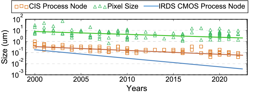
Moving computation inside a CIS, however, is not without challenges. Most importantly, processing inside the sensor is far less efficient than that outside the sensor, fundamentally because the CIS process node significantly lags behind that of the conventional CMOS. Fig. 3 illustrates this difference, where square markers show the process nodes used in CIS designs from all ISSCC papers appeared during Year 2000 and Year 2022, which include leading industry CIS designs at different times. We overlay a trend line regressed from these CIS designs to better illustrate the scaling trend. As a comparison, the blue line at the bottom represents the conventional CMOS technology node scaling laid out by International Roadmap for Devices and Systems (IRDS) (ird, [n. d.]).
At around Year 2000, the CIS process node started lagging behind that of the conventional CMOS node, and the gap is increasing. CIS design today commonly use 65nm and older process nodes. This gap is not an artifact of the CIS designs we pick; it is fundamental: there is simply no need to aggressively scale down the process node because the pixel size does not shrink much. The triangles in Fig. 3 represent the pixel sizes of all the CIS designs we surveyed. The slope of CIS process node scaling almost follows exactly that of the pixel size scaling. The reason that pixel size does not shrink is to ensure light sensitivity: a small pixel reduces the number of photons it can collect, which directly reduces the dynamic range and the Signal-to-Noise ratio (SNR) (Bigas et al., 2006).
Inefficient in-sensor processing can be mitigated through 3D stacking technologies (Xie and Zhao, 2015), which allows for heterogeneous integration: the pixel layer and the computing layer(s) can use their respective, optimal process node. Stacking, however, could increase power density especially when future CIS integrate more processing capabilities. Therefore, harnessing the power of (stacked) computational CIS requires exploring a large design space and address key challenges, some of which we list below. Providing a tool to easily navigate the design space is the goal of our CamJ framework.
-
•
Whether and what to compute in vs. off CIS?
-
•
How to architect each layer in stacked CIS to achieve energy reduction without increasing power density?
-
•
What to compute in the analog vs. digital domains?
3. CamJ Framework
No framework to date allows designers to explore the complicated design space of computational CIS at a system level. Our CamJ framework is designed to fill this void (Sec. 3.1). We first outline the design principles of CamJ, followed by an overview of the CamJ design internals (Sec. 3.2). We use a concrete example to demonstrate from a designer perspective how CamJ is used (Sec. 3.3).
3.1. When is CamJ Used in the Design Cycle?
CamJ is meant to be used for system-level exploration after each component design is sketched out; an analogy would be Systems-on-a-Chip (SoC) vs. accelerator design. Before system-level exploration, a team usually has at hand a range of component-level designs, which could be licensed Intellectual Property (IP) blocks, reference designs from the literature, or earlier designs from other teams in the organization (e.g., using a synthesis flow or High-Level Synthesis tools); in all cases the component-level energy behavior is known or can be modeled using external tools like Aladdin (Shao et al., 2014) and OpenRAM (Guthaus et al., 2016).
CamJ helps designers make design decisions when assembling the individual (digital and analog) components into an optimal system. Ideally, a designer uses CamJ to estimate the system energy given initial designs of individual components; using the estimation, a designer can iteratively refine the components/system design. For instance, CamJ can identify energy bottlenecks and guide the re-design of corresponding components. Orthogonally, a designer can use CamJ to explore optimal mapping and partitioning of the algorithms between analog vs. digital domains or in vs. off CIS to minimize overall system energy under performance targets.
CamJ is not a synthesis tool; it does not generate (nor estimate the energy of) an accelerator. Rather, CamJ can be used in conjunction with HLS: one could use HLS to first generate an accelerator and then use CamJ to explore, in the bigger system, how/whether that accelerator would fit in a computational CIS to maximize end-to-end application gains.
3.2. Design Principles and Overview
As with any energy modeling tool (Brooks et al., 2000; Leng et al., 2013; Kandiah et al., 2021), the total CIS energy is sum of the product of 1) the access count to each hardware unit and 2) the per-access energy consumption. Therefore, the central objective of CamJ is to develop a modeling methodology that accurately estimates those two statistics using a programming interface that, critically, only requires user inputs for information that cannot be automatically inferred. Fig. 4 shows an overview of the CamJ framework. Sec. 3.3 and Sec. 4 discuss the programming interface and modeling details, respectively. Here, we provide an overview of the interface and modeling methodology.
Interface.
CamJ’s interface also decouples the description of an algorithm, the underlying hardware, and the mapping between the two. A decoupled interface facilitates an iterative system design process, during which algorithm, hardware, and algorithm to hardware mapping can change independently. For instance, one can evaluate algorithmic changes by re-writing the algorithm description without touching the hardware design, or explore different algorithm-to-hardware mappings (e.g., split between analog vs. digital and between in vs. off sensor) by describing a new mapping.
Internal Modeling.
One might be surprised to find that CamJ directly asks for the per-cycle/access energy of the digital structures. This is because of the design philosophy of CamJ (Sec. 3.1): it is not used to generate digital accelerators; rather, it helps assess how an accelerator fits in the entire computational CIS system. For that reason, CamJ expects designers to have a preliminary design of the digital accelerators (whether it’s your manual design, HLS generated, or a licensed IP), in which case one will have the per-cycle/access energy statistics.
Unlike digital structures, few energy modeling tool exists for analog structures, whose energy consumption ( ) depend on many low-level circuit details (e.g., load capacitance, gain, bias current) that are cumbersome and perhaps unreasonable to ask system-level designers for. Our design decision is to expose a low-level interface to accept these parameters from expert users, but also provide default energy models based on classic implementations of analog components and delay analyses of these components (Sec. 4.1).
Finally, CamJ performs a series of pre-simulation design checks to ensure that the algorithm and hardware combination 1) is functionally viable (e.g., ADCs must exist between the analog and digital domain), 2) does not have pipeline stalls (to avoid accumulating long frame latency), and 3) has well-formed dependencies in the algorithm DAG (e.g., no circle). We provide feedback upon check failures and a detailed energy breakdown, which helps designers iteratively refine the algorithm and/or hardware.
3.3. Programming Interface
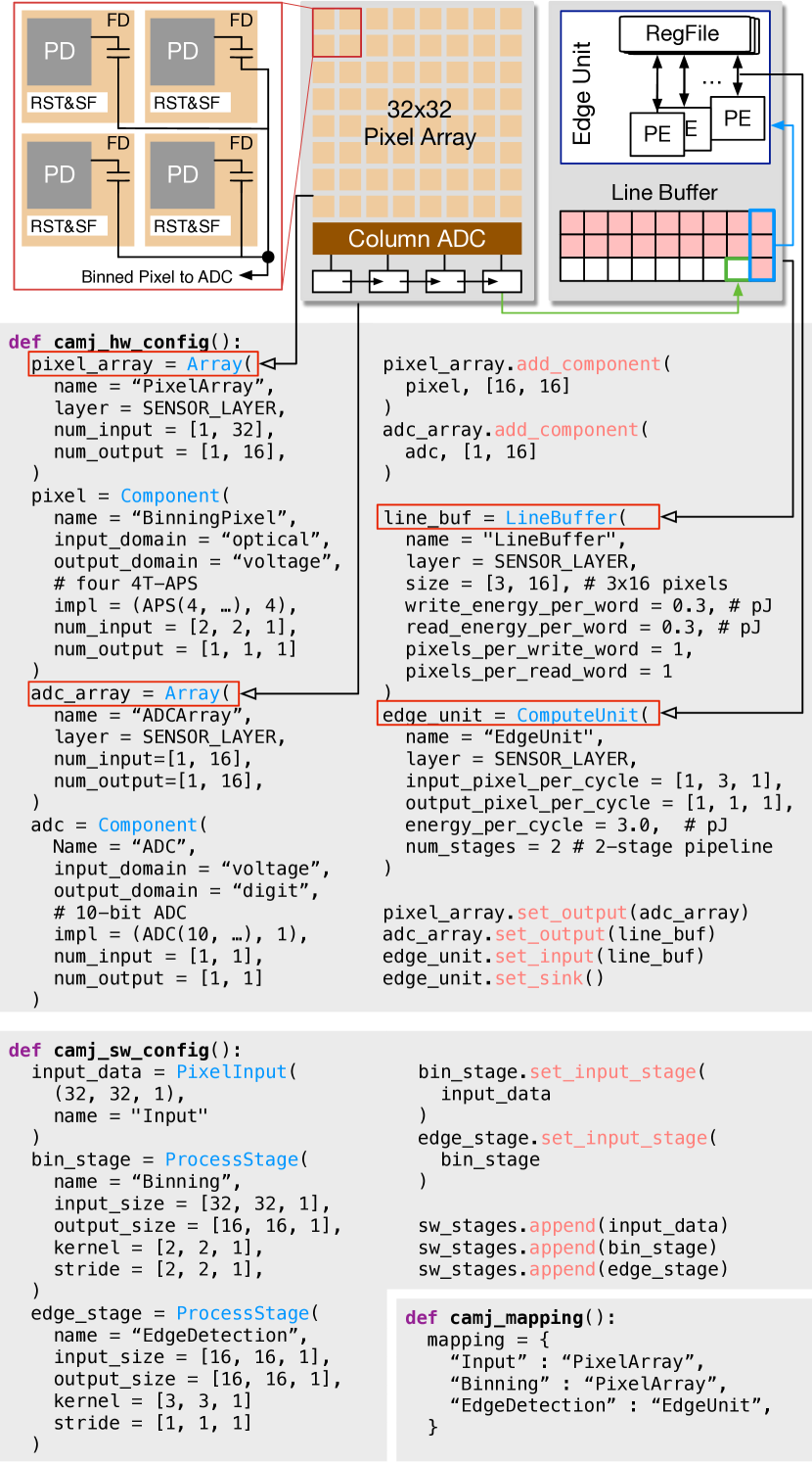
We use a running example in Fig. 5 to introduce the programming interface and illustrate the main design decisions.
An Example.
The Python code in Fig. 5 shows a concrete example to use the programming interface of CamJ. In this conceptual CIS design with a pixel array, every pixel tile is first averaged (i.e., “binned”) to produce a image. The sensor then performs a digital edge detection on the image before sending the edge data through the MIPI CSI interface. The camj_hw_config function and the camj_sw_config function describe the hardware components and the algorithm, respectively. The camj_mapping maps each algorithm stage to a hardware component. We explain each part next.
Algorithm Description.
The code in camj_sw_config describes the DAG of the entire processing pipeline, starting from the raw pixels generated by the pixel array (PixelInput), which go through two processing stages: bin_stage for pixel binning and edge_stage for edge detection. The set_input_stage method connects the stages together to form a DAG.
Notice how the algorithm description does not require the actual arithmetic details; we observe that image processing algorithms can be abstracted as stencil operations that operate on a local window of pixels at a time (Hegarty et al., 2014; Qadeer et al., 2013) — convolution (or image filtering in conventional image processing parlance) being a prime example. This observation holds in all the ISSCC/IEDM papers since Year 2000 we surveyed. Irregular computations complicate hardware design and increase energy, defeating the purpose of in-CIS computing.
Therefore, users express only the input/output image dimensions (input_size, output_size) along with the stencil window (kernel) and stride size (stride). Given the regular computation and data access pattern of stencil operations, CamJ could accurately estimate the access counts to different hardware structures for energy estimations. Nonetheless, CamJ does accept as input a memory trace offline collected for an irregular algorithm, which can then be integrated with external tools such as DRAMPower (Chandrasekar et al., 2012) to estimate the energy consumption for irregular algorithms.
Hardware Description.
camj_hw_config describes the hardware architecture, which we illustrate at the top of Fig. 5. The hardware description consists of two components: analog processing units and digital processing units.
Analog Units. CIS hardware necessarily starts from analog units, which, at a high level, are described as a set of Analog Functional Arrays (AFA), which is in turn is composed of a set of Analog Functional Components (A-Components). The most important AFA in a CIS is the pixel array (pixel_array), in which each A-Component is a pixel, which is added to the pixel array through the add_component method. In the example of Fig. 5, the pixel array is followed by another AFA, i.e., the ADC array (adc_array), where each A-Component is an ADC.
|
Digital | ||||||
|---|---|---|---|---|---|---|---|
| Memory |
|
|
|||||
| Compute |
|
|
From users’ perspective, each A-Component performs a particular kind of (arithmetic) operation. In addition to a pixel or an ADC, CamJ provides other common A-Components used in CIS such as MAC or logarithmic operations. The complete list of analog A-Components is in Tbl. 1. The energy consumption of each A-Component, which is dictated by its circuit-level implementation, is abstracted away from the users by the impl method. Sec. 4.2 will later describe how we model the energy of each A-Component by mapping it to its analog circuit implementation.
What users do have to provide, however, is the signal dimension (num_input and num_output) and signal domain (input_domain and output_domain) of an AFA’s input and output data. These parameters allow CamJ to check whether the simulated CIS is functionally viable. Specifically, the input_domain of a consumer unit and the output_domain of a producer unit must match. If, for instance, the producer is in the charge domain and the consumer is in the voltage domain, CamJ will ask designers to insert a charge-to-voltage conversion component111unless the output of the consumer is in the voltage domain, where the inherent capacitor of the consumer naturally acts as an analog buffer., which has energy implications. Similarly, if the num_input of a consumer unit and the num_output of a producer unit do not match, the hardware must have an analog buffer in-between, which, again, could have energy implications.
Digital Units. The digital part of the hardware is described by specifying a set of compute units that communicate through memory structures. In this example, the compute unit is the edge detection accelerator (instantiated through ComputeUnit), which reads from the line buffer (LineBuffer), a pre-defined memory structure, that stores data from the pixel array, an analog unit as described before.
Column 2 of Tbl. 1 lists the memory structures and compute units available in CamJ. We support three memory structures commonly found in image/vision processing: FIFO (FIFO), line buffer (Hegarty et al., 2014; Whatmough et al., 2019) (LineBuffer), and double-buffered SRAM (DoubleBuffer). The compute units are abstracted as pipelined accelerators through the ComputeUnit interface. We also provide a SystolicArray class to describe a systolic array due to its importance in executing DNNs.
With the generic pipelined accelerator interface (ComputeUnit), users can model a wide range of (image processing) accelerators. To describe a pipelined accelerator, CamJ requires three main parameters: the shape of pixels read per cycle (input_pixel_per_cycle), the shape of pixels generated per cycle (output_pixel_per_cycle), and the pipeline depth (num_stages). Using these statistics, CamJ performs cycle-level simulation for two purposes. First, CamJ can check whether the accelerator will stall the CIS pipeline and, if so, asks for a re-design of the accelerator. Second, CamJ can estimate the total latency of the digital domain, which is critical for analog energy estimation. Stall checking and latency estimation are critical for analog energy estimation as we will discuss in Sec. 4.1.
Mapping.
The camj_mapping function maps each algorithm stage to a hardware unit. The code is self-evident. Users can simply remap the algorithm to hardware to explore a different system design. The decoupling of algorithm and hardware description through the mapping function also enables easy expression of hardware reuse—by simply mapping different algorithm nodes to a hardware component.
4. Energy Modeling Methodology
The energy consumption per frame of a CIS sensor is the sum of that of the analog, digital, and data communication:
| (1) |
Before we describe how the analog component (Sec. 4.2), digital component (Sec. 4.3), and communication component (Sec. 4.4) are modeled separately, we first discuss a prerequisite of energy modeling: delay estimation (Sec. 4.1).
4.1. Delay Estimation
The energy consumption, both analog and digital, is correlated with the circuit speed. For example, in the analog domain an operational amplifier (OpAmp) with higher response speed requires larger bias current, which increase the energy consumption (assuming the OpAmp is active over a fixed duration, e.g., when used for an analog frame buffer). The latency of digital units is estimated through cycle-level simulation as described in the previous section. The delay of an analog unit, in contrast, depends on many parameters specific to a fully-designed circuit. We find it cumbersome and error-prone to ask users for input: users often find themselves tuning low-level parameters only to end up with a design that misses the target frame rate. Instead, CamJ’s insight is that each analog unit’s delay can be automatically inferred from the prescribed frame rate.
Specifically, the fundamental observation that CamJ relies on is that the CIS pipeline is designed to never stall. This is because the input data to the pipeline is generated at a constant rate as the pixel array is exposed to light at the constant speed. If the pipeline ever stalls in a later stage, the frame latency would gradually accumulate, leading to excessively long responsive latency or frame drops. Therefore, CIS designers ensure that the hardware pipeline never stalls. In a fully-pipelined hardware, each pipeline stage must have roughly the same delay; this is the basis of our delay estimation.
Example.
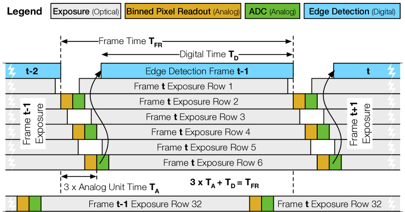
Fig. 6 shows the pipeline timing for the example in Fig. 5. The frame time is 1/FPS, where FPS is the target frame rate. In the diagram, the frame time is the delay between when the pixels of the current frame can be read-out to when the computation of the current frame finishes. The “Binned Pixel Readout” and “ADC” are the two analog units, who share the same delay (i.e., balanced pipeline) to be estimated. The “Edge Detection” is the digital unit, which starts once the second line has been written to the line buffer.
To estimate , we first simulate the digital domain to estimate the latency of the entire digital domain ( here). Given the frame time , we can then estimate how much time is left for the analog units. In this example, .
CamJ will analyze the hardware description and, upon detecting potential stalls, asks the user to re-design the hardware to avoid stall. Specifically, CamJ checks to avoid three scenarios: 1) pixel required is not generated by the producer yet, 2) the memory in-between two stages is full, or 3) the number of access ports in the memory structures is not enough.
4.2. Analog Energy Modeling
The analog energy per frame, , is the sum of the energy consumption per access of each A-Component weighted by the access count to that component. Refer to Tbl. 1 for a list of A-Components that CamJ supports.
| (2) |
Modeling A-Components Access Count.
The access count to a A-Component is the number of times the A-Component is used per frame. Recall from Sec. 3.3 that each A-Component is part of an Analog Functional Array (AFA). CamJ leverages the fundamental observation that stencil operations in image processing have regular computation and memory access patterns and, thus, the access count to each A-Component in the same AFA is the same.
As a result, the access count of a component is simply the ratio between the total number of operations mapped to the AFA that contains the component () and the number of components in that AFA ():
| (3) |
The numerator is easily derived from the algorithm description of a stencil operation (e.g., calculating the number of MAC operations in a convolution). The denominator is the num_component attribute of the AFA (see Fig. 5).
Modeling A-Components Access Energy.
Internally, each A-Component is built from a set of analog cells, which we call A-Cells. Modeling per-access energy of an A-Component requires knowing its cell-level implementation. Expert users can define new cell parameters and/or cell-level implementation of an A-Component. Absent those, each A-Component has a default implementation, surveyed from classic and recent CIS designs (Hsu et al., 2020; Park et al., 2021; Kaur et al., 2020; Young et al., 2019; Yang et al., 2015). For instance, a 4T-APS pixel A-Component consists of a photodiode (PD) A-Cell, a floating diffusion node (FD) A-Cell, and a source follower (SF) A-Cell; a multiplier implemented by switched-capacitor charge re-distribution (Lee and Wong, 2017) consists of a capacitor array A-Cell and an OpAmp A-Cell.
We now describe our energy modeling of A-Components, but keep in mind that these design details are abstracted away from typical users. is the weighted sum of the energy consumption of each constituting A-Cell in the component and the access counts to the A-Cell:
| (4) |
Despite large varieties of high-level analog circuits, the A-Cell used for analog in-sensor computing can be categorized to three classes according to circuit characteristics: dynamic A-Cell, static-biased A-Cell, and non-linear A-Cell. They each consume energy in a different way.
Dynamic A-Cell. The energy of a dynamic circuit comes from the charging and discharging of the total capacitance in the circuit:
| (5) |
where represents the total number of capacitance nodes in the dynamic circuit, and and are the capacitance and the voltage swing at capacitance node, respectively. Typical dynamic A-Cells include capacitive digial-to-analog converter (CDAC) and passive analog memory.
In Equ. 5, is determined by the analog supply and the number of transistors placed between the analog supply and the ground. The nodal capacitance is determined by its thermal noise and the computation precision. To guarantee the accuracy of analog computing, the maximum thermal noise should be kept below LSB of the data resolution:
| (6) |
where . Data resolution is algorithm dependent. For example, if and the required resolution is 8-bit, the thermal noise should be less than , from which is obtained.
Static-biased A-Cell. The energy of a static-biased circuit comes from the integration of the bias current over a specific time period under the analog supply :
| (7) |
where is the bias current and is the time during which the A-Cell is statically biased.
We provide two ways to estimate based on circuit details. For A-Cells where directly drives the load capacitance (e.g. static-biased SF in a pixel), is determined by charging up the load within the given time:
| (8) |
where is the load capacitance. The energy is reduced to:
| (9) |
For A-Cells where does not directly drive the load capacitance (e.g. differential operational amplifier in analog memory or discrete-time integrator), can be determined by the classic method (Jespers, 2010):
| (10) |
where is a technology-insensitive factor ranging from 10 to 20 depending on the inversion level of the transistors, and GBW is product between gain (G) and bandwidth (BW).
To use Equ. 7 and Equ. 10, CamJ must estimate BW and , both of which depend on the A-Cell delay. Specifically, BW is the reciprocal of the A-Cell delay and is:
| (11) |
where is the delay of the A-Component containing the A-Cell and is estimated in Sec. 4.1; is the number of cells before the current A-Cell on the A-Component critical path, and is the delay of an A-Cell. Absent timing condition from users, we evenly allocate the A-Component delay to each A-Cell, based on the fact that the analog signal uni-directionally flows through the A-Components we support so all A-Cells are on the critical path.
Non-linear A-Cell. For those circuits with non-linear transfer functions, such as ADCs and comparators (which are essentially 1-bit ADCs), they contain both dynamic/static-biased circuit cells and digital logic so it is difficult to estimate the energy from analytical formulas. Instead, we use the ADC’s Walden Figure-of-Merit (FoM) plot (Murmann, [n. d.]) surveyed from recently published CIS papers, which shows the ADC’s energy-per-conversion vs. its sampling rate. Specifically, given the ADC sampling rate (the reciprocal of the A-Cell delay) we, absent detailed user input, use the median energy-per-conversion at that sampling rate as the estimation. The total energy of non-linear A-Cell is thus obtained by the product of its estimated FoM and the number of required conversions:
| (12) |
The access counts to a specific A-Cell are the number of times the A-Cell is used along both the spatial and temporal scale to generate one A-Component output:
| (13) |
For example, if an A-Cell represents an static-biased SF in a pixel, would be the number of SFs in the pixel and would be the number of times the pixel charge is read out (e.g., 2 if correlated double sampling is used to reduce noise (Capoccia et al., 2020)). The access counts information for A-Cells is hard-coded for each A-Component and is abstracted away from typical users, but can be updated for a custom design.
| CIS | Process Node | Stacked | Analog | Digital | |||||
|---|---|---|---|---|---|---|---|---|---|
| Pixel | Memory | PE Operation | PE Position | Op Domain | Memory | PE Size | |||
| ISSCC’17 (Bong et al., 2017a) | 65nm | No | 3T APS | Avg&Add | Column&Chip | Charge&Voltage | 160KB | ||
| JSSC’19 (Young et al., 2019) | 130nm | No | 4T APS | Logarithmic Sub. | Column | Voltage | - | - | |
| Sensors’20 (Choi et al., 2020) | 110nm | No | 4T APS | No | MAC&MaxPool | Column | Voltage | - | - |
| ISSCC’21 (Eki et al., 2021) | 65nm/22nm | Yes | 4T APS∗ | No | - | - | - | 8MB | |
| JSSC’21-I (Hsu et al., 2020) | 180nm | No | PWM | No | MAC | Column | Time&Current | - | - |
| JSSC’21-II (Park et al., 2021) | 110nm | No | 4T APS | No | MAC | Column | Charge | - | - |
| VLSI’21 (Seo et al., 2021) | 65nm/28nm | Yes | DPS | No | - | - | - | 6MB | - |
| ISSCC’22 (Hsu et al., 2022) | 180nm | No | PWM | No | MAC | Column | Time&Current | 256B∗ | 1 |
| TCAS-I’22 (Xu et al., 2021) | 180nm | No | 3T APS | No | Mul.&Add | Pixel&Chip | Current | - | - |
4.3. Digital Energy Modeling
The digital energy of a frame is the sum of the computation energy of each compute unit and the energy of each memory structure :
| (14) |
The energy of each compute unit is the product of the energy per cycle and the number of cycles :
| (15) |
We rely on users to provide , which usually is obtained through HLS/ASIC synthesis flows. The cycle counts, in contrast, are obtained through cycle-level simulation by CamJ.
The energy consumption for memory accesses is the sum of leakage energy and the dynamic access energy; the latter is the product of the energy consumption for one memory read or write () and the total number of memory reads () or writes ():
| (16) |
The leakage energy is the product of the leakage power and the memory active time (i.e., not power-gated), which is a fraction of the frame time . Users supply the dynamic read/write energy and leakage power; the access counts and the active time are from the CamJ simulation.
4.4. Communication Energy Modeling
The communication power is dominated by the energy to transfer the data outside the sensor using the energy-hungry MIPI CSI-2 interface and, in the case of 3D-stacking CIS, the energy of TSV. In literature the energy of the two interfaces is usually given for energy per Byte. Therefore, the communication energy is given by:
| (17) |
and are user supplied with represented data reported in the literature (Liu et al., 2019). The data volume statistics in both interfaces are generated in CamJ simulation (based on the algorithm description and algorithm to hardware mapping).
5. CamJ Validation
In this section, we validate CamJ against real measurement data from nine recent CIS chips (Bong et al., 2017a; Young et al., 2019; Choi et al., 2020; Eki et al., 2021; Hsu et al., 2020; Park et al., 2021; Seo et al., 2021; Hsu et al., 2022; Xu et al., 2021) shown in Table 2. These designs span a range of design dimensions including 2D and 3D designs, different process nodes, pixel types, as well as PE designs and memory sizes in the analog and digital domains.
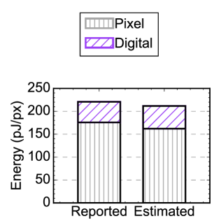
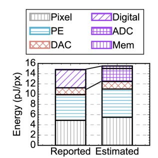
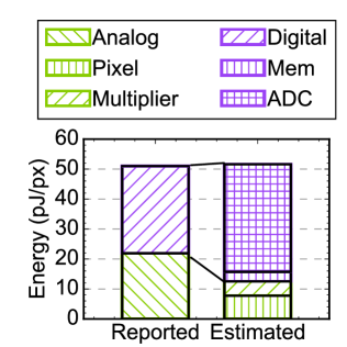
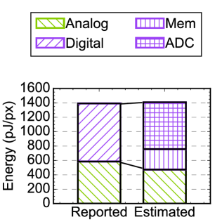
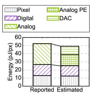
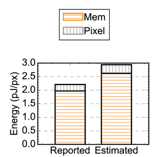
Fig. 7 compares the estimated and actual energy per pixel reported in the original papers. Our estimations closely match the measured results, which span several orders of magnitude, showing both the diversity of the CIS design styles and the wide system power/energy scale that CamJ can flexibly support and accurately model. Across all designs, CamJ achieves a Mean Absolute Percentage Error of 7.5% and a Pearson Correlation Coefficient of 0.9999.
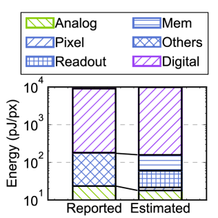
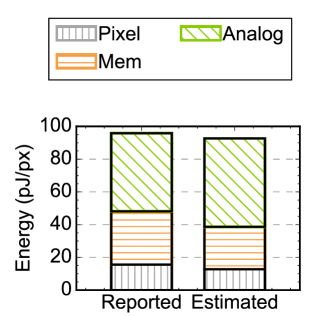
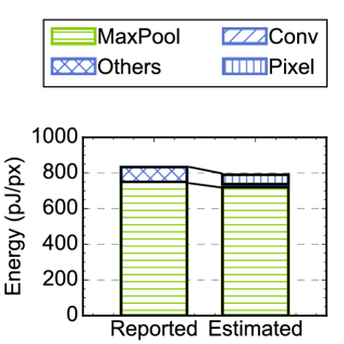
Fig. 7b – Fig. 7j compare the detailed energy breakdown across the nine designs. Whenever possible, we use the circuit parameters reported in the papers. For SRAMs, we use DESTINY (Poremba et al., 2015) to obtain per-access energy. The three papers that perform digital computation all execute DNNs, where a PE is a MAC unit; we use the synthesis result of a 65 nm MAC unit design for per-MAC energy (Bong et al., 2017a), and scale it to other process nodes based on classic CMOS scaling (Stillmaker and Baas, 2017; Sarangi and Baas, 2021).
While overall CamJ provides an accurate component-level and full-system energy estimation, we find two key reasons behind result mismatches. First, the results are less accurate when CamJ does not have access to detailed design parameters. For example, the pixel estimation in Fig. 7f, Fig. 7g, and Fig. 7j shows an absolute error of 12.4%, 38.9%, and 33.3%, respectively, due to insufficient circuit parameters on pixel ramp-generator (Fig. 7f), pixel parasitic capacitance (Fig. 7g), and photodiode voltage swing (Fig. 7j). Similarly, the analog PE in Fig. 7f and Fig. 7b shows an absolute error of 9.3% and 23.7% due to insufficient circuit parameters on sampling capacitance (Fig. 7f) and sense amplifier conversion energy (Fig. 7b), respectively. In contrast for Fig. 7c, where the detailed design parameters are provided for the analog PE, the estimation error is only 0.4%.
The other source of inaccuracy comes from the mismatch between the actual circuit design and CamJ’s default circuit template. For example, the ADCs in Fig. 7g and Fig. 7h show an absolute difference of 31.7% and 16%, respectively 222Both papers consider ADC as a digital unit, which is what we use here.; the original designs use low-power dynamic technique (Fig. 7g) whereas CamJ estimates the energy of ADC based on the FOM survey (Murmann, [n. d.]). The memory in Fig. 7j shows an estimation error of 33.0% because the original design uses customized 8T SRAMs while CamJ uses standard 6T SRAMs from DESTINY (Poremba et al., 2015), resulting in higher leakage power.
6. Architectural Exploration
We now demonstrate three complementary examples of using CamJ to explore architectural trade-offs. The three use-cases complement each other. First, we explore when moving computation inside the CIS brings energy benefits (Sec. 6.1). We show that the energy reduction is small in a conventional 2D design. We then show that introducing 3D stacking, which allows for hybrid integration, further improve the energy efficiency at a cost of higher power density (Sec. 6.2). Finally, we discuss the trade-off of moving computation into the analog domain (Sec. 6.3).
6.1. Computing Inside vs. Off Sensor

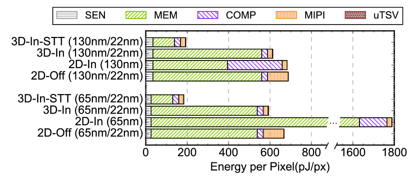
Computing inside CIS reduces the data transmission cost by consuming pixel data inside the sensor. To explore the benefits, we evaluate two recent papers, Rhythmic Pixel Regions (Kodukula et al., 2021b) and Ed-Gaze (Feng et al., 2022), both of which generate a small Region of Interest (ROI) from the original full-resolution image and, thus, can potentially benefit from in-sensor computing by moving the ROI generation inside the sensor.
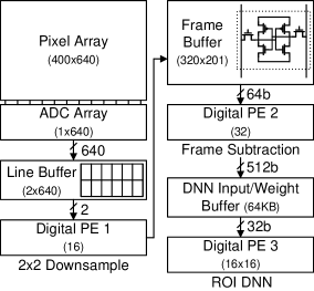
Fig. 8a and Fig. 8b illustrate the execution flow of the two algorithms, respectively. Everything after the ADC is executed outside the sensor in the original papers, and we use CamJ to evaluate the energy consumption after moving the entire execution inside the sensor. Specifically:
-
•
Rhythmic Pixel Regions: a pixel array is processed by a dedicated accelerator (Compare & Sample) to generate the ROI, which on average reduces the image size by 50%. The ROI generation performs roughly arithmetic operations per frame.
-
•
Ed-Gaze: a pixel array is first downsampled by , and then processed by an pixel-wise subtraction operation with respect to the previous frame to generate an event map, which is then processed by a DNN to generate the ROI. The ROI, on average, reduces the image size by 25%. The DNN dominates the computation and performs about MAC operations per frame.
We use CamJ to evaluate two hardware configurations:
-
•
2D-In (H): a 2D CIS fabricated in the H process node; the entire execution is performed inside the CIS.
-
•
2D-Off (H/L): a 2D CIS fabricated in the H process node; everything after the ADC takes place on an SoC, which is fabricated in the L process node. We evaluate two CIS process nodes, 130 nm and 65 nm, both common in CIS designs (Tbl. 2). We set the SoC process node to 22 nm.
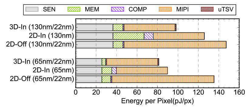
Fig. 9a shows the energy of Rhythmic Pixel Region under different designs. Overall, 2D-In reduces the energy compared to 2D-Off. When CIS process node is 130nm, 2D-In saves 14.5% compared to 2D-Off. This saving improves to 33.4% when the CIS process node is 65nm. The energy reduction comes from reducing the amount of data (full-resolution image vs. ROI) that has to be communicated through the MIPI CIS-2 interface (MIPI in the figure). This data communication cost reduction comes at the expense of increasing the computation (COMP) and memory access (MEM) cost, both of which increase because of the older process node in the CIS.
Ed-Gaze’s results are shown in Fig. 9b, which tells a different story. Computing inside the CIS ends up consuming much more energy than computing on the SoC. This is because communication cost is light for Ed-Gaze: the communication cost contributes to only 15.0% of the total energy in the off-sensor system to begin with. Thus, the additional energy costs of computation and memory accesses inside the sensor far outweigh the reduction in communication cost. Interestingly, 65nm 2D-In consumes more energy than its 130nm counterpart, because the 65nm node is known to have high leakage power (Gielen and Dehaene, 2005). In Ed-Gaze, the frame buffer must be on during the entire frame time without power gating, since a frame must always be retained in order for frame subtraction.
Finding 1: Computation inside CIS is less efficient than that off CIS. In-CIS computing saves energy only when the process node of the CIS is not too far behind that of the SoC and the application is communication-dominant.
6.2. Comparison of 2D CIS and 3D-stacked CIS
We use CamJ to explore the benefits of 3D stacked CIS. We use the same algorithms in Rhythmic Pixel Regions and Ed-Gaze and consider two additional 3D configurations:
-
•
3D-In (H/L): a two-layer stacked CIS, where the pixel layer is fabricated in the H process node and the compute layer is fabricated in an advanced process node L. All post-ADC operations take place in the compute layer.
-
•
3D-In-STT (H/L): similar to 3D-In (H/L) except the SRAM in the compute layer is replaced with a STT-RAM, which we model using NVMExplore (Pentecost et al., 2022). Rhythmic Pixel Regions lacks STT-RAM results, because it requires only a 2K memory, which NVMExplore does not support.
Comparing 3D-In and 2D-In in Fig. 9a shows that 3D integration reduces the energy by 15.8% on average for Rhythmic Pixel Regions. This is because the digital PEs and the SRAMs now use the same process node as that of the SoC; moving computation inside the sensor no longer increases the computation and memory energy but still enjoys the significant data volume reduction. The additional cost of moving data via TSV is insignificant, due to the low energy cost of TSV.
The energy reduction from 3D integration is even higher for Ed-Gaze. Comparing 3D-In and 2D-In in Fig. 9b, 3D stacking reduces the energy by 38.5% on average, because memory energy contributes to 71.3% of the total energy in 2D-In, which is significantly reduced when using a 22nm node.
That said, the memory energy still dominates in 3D-In, because the frame buffer cannot be power-gated as explained before, consuming non-trivial leakage power. To further reduce the memory energy, we explore STT-RAM, which is known to have low leakage. By replacing SRAM with STT-RAM, 3D-In-STT further reduces the overall energy by 69.1% and 68.5% compared to 3D-In under the 65nm/22nm and the 130nm/22nm combination, respectively.
| Process Node | Rhythmic Pixel Regions | Ed-Gaze | ||||
|---|---|---|---|---|---|---|
| Pixel/Compute | 2D-Off | 2D-In | 3D-In | 2D-Off | 2D-In | 3D-In |
| 130nm/22nm | 0.05 | 0.09 | 0.06 | 0.19 | 0.30 | 0.78 |
| 65nm/22nm | 0.03 | 0.05 | 0.04 | 0.11 | 2.24 | 0.70 |
Power Density.
While 3D stacking is known to increase power density, we use CamJ to show that the impact on power density is algorithm-specific. We use a conservative area estimation to obtain a power density upper bound while leaving a comprehensive area modeling to future work. Specifically, we use the pixel array to approximate the analog area and use SRAM area to approximate the digital area.
Tbl. 3 compares the power density across the three sensor variants for the two algorithms. The power density of Rhythmic Pixel Regions shows no significant difference among the three variants, because the power of Rhythmic Pixel Regions is dominated by communication, which is not greatly affected by stacking. In contrast, the power density of Ed-Gaze more than doubles by 3D stacking under the 130nm/22nm combination. This is because 3D-In is 3 smaller in area than 2D-In. Under the 65nm/22nm combination, 2D-In has higher power density due to the high leakage power of 65nm process, which is avoided in the stacked design.
It is worth noting that the absolute power density of 3D-stacked sensors is still very low, in fact three to four orders of magnitude lower than the power density of typical CPUs (up to 1 (Danowitz et al., 2012)) and GPUs (up to 0.3 (Chen, 2009)). Such a low power density will unlikely lead to thermal hotspots and create a cooling challenge (Yu and Wu, 2018). However, higher power density increases the thermal-induced noise and worsens the imaging and computing quality (Kodukula et al., 2021a). End-to-end application optimization must take into account the noise impact, an exploration that CamJ enables and that we leave to future work.
Finding 2: 3D stacking saves energy but increases power density — for compute-dominant applications. The absolute power density is not high enough to create thermal hotspots but could increase noise, warranting further studies.
6.3. Comparison of Analog and Digital Computing

We use CamJ to explore the benefits of in-sensor analog computing. In particular, we use Ed-Gaze for the case study and consider a mixed-signal configuration:
-
•
2D-In-Mixed: a 2D CIS, where the first two stages in the algorithm (Fig. 8b), downsampling and frame subtraction, are implemented in analog while last stage (ROI DNN) is implemented in the digital domain.
Fig. 10 shows how the Ed-Gaze is mapped to a mixed-signal CIS. Inside the pixel array, the downsampling is done through pixel binning (similar to that in Fig. 5). The analog frame buffer stores the downsampled analog pixel values, which are read by an analog PE array for frame subtraction. Each analog PE consists of a switched-capacitor subtractor/ multiplier for absolute subtraction and a comparator for frame delta digitization. The output of the Analog PE array enters the SRAM array, at which point the hardware is the same as that in 2D-In. For a fair comparison and to ensure area overhead is well accounted for, we conservatively set all the capacitors to 100fF. Despite the over-sizing, analog design still yields at least 27% less area than the digital counterpart.
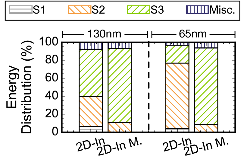
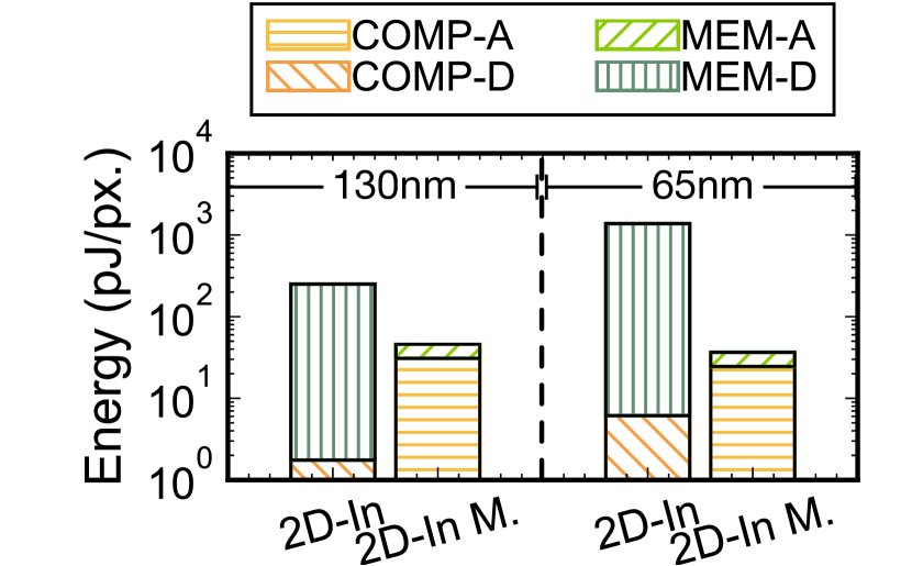
Fig. 11 compares 2D-In-Mixed and 2D-In. Moving the first stages of the Ed-Gaze algorithm to the analog domain reduces the energy by 38.8% and 77.1%. The energy reduction comes from two sources: removing the ADCs (indicated by lower SEN) and replacing SRAMs in the first two stages with analog buffers (indicated by lower MEM-D). The reduction in MEM-D is particularly significant for the 65nm node, where the SRAM leakage power is high. To corroborate the results, Fig. 13 shows the normalized energy breakdown among the three stages (S1, S2, and S3). S3 (DNN) becomes the dominant stage after moving first two stages into analog domain, showing the effectiveness of analog processing.
Interestingly, the energy reduction is obtained when the compute energy of the first two stages slightly increase. Fig. 13 shows the energy breakdown of the first two stages. While the memory energy reduces, the compute energy increases in the mixed-signal mode. This is because to maintain an 8-bit precision the OpAmp consumes too much energy (Equ. 6). A caveat is that the analog design presented here, which uses active switched-capacitor circuits, is based on our specific implementation choice. It is conceivable that different designs would yield different efficiency results.
Finding 3: While analog computing is known for reducing ADC and computing energy, the energy saving is also attributed to lower analog memory energy, especially for memory-intensive applications, which many in-CIS use-cases are.
7. Related Work
Power Modeling.
Power/energy modeling is a cornerstone of architectural exploration. Prior power models of CPUs (Brooks et al., 2000; Li et al., 2009; Shao and Brooks, 2013), GPUs (Leng et al., 2013; Kandiah et al., 2021; Hong and Kim, 2010), and memory (Balasubramonian et al., 2017; Poremba et al., 2015; Guthaus et al., 2016; Pentecost et al., 2022) have enabled a plethora of power/energy optimizations. Fundamentally, CamJ shares the same, bottom-up modeling methodology, where energy is estimated from access counts and per-access energy. Additionally, CamJ provides a clean programming interface to integrate other architectural simulators (Shao et al., 2014; Samajdar et al., 2018; Feng et al., 2019; Gao et al., 2017) and memory modeling tools (Poremba et al., 2015; Pentecost et al., 2022) to model bespoke accelerators and memories.
Prior analog power modeling requires either detailed transistor-level parameters (Svensson and Wikner, 2010) or is based on the statistic models of particular analog circuits (Lauwers and Gielen, 2002). Lim et al. (Lim and Horowitz, 2019) decomposes a mixed-signal circuit into basic cells and accelerate the mixed-signal simulation by approximating the transfer function of each cell. CamJ uses a similar decomposition methodology but specifically targets CIS.
CIS Modeling.
No comprehensive CIS modeling framework exists. Two recent papers from Meta use first-order analytical model to estimate the energy of their custom CIS design, i.e., 3D stacking with DPS (Gomez et al., 2022; Liu et al., 2019). It does not provide the level of flexibility to accommodate general CIS design and architecture exploration as supported by CamJ.
LiKamWa et al. (LiKamWa et al., 2013) provide a coarse-grained CIS power model using the idle and active period/power without considering the hardware implementation details. CamJ, instead, models the hardware with finer granularity to achieve finer-grained architectural exploration. Kodukula et al. (Kodukula et al., 2021a) cite coarse-grained component energy of typical CIS designs and builds a thermal model. CamJ, can provide more accurate power/energy modeling that feeds into such thermal model.
Visual Computing Optimizations.
Recent work discusses the possibility of processing inside an CIS to reduce the data transmission cost, e.g., Ed-Gaze (Feng et al., 2022), Rhythmic Pixel Regions (Kodukula et al., 2021b), Reid et al. (Pinkham et al., 2020), and SplitNets (Dong et al., 2022). All, however, rely on first-order energy models. Using CamJ, we study the algorithms in Ed-Gaze and Rhythmic Pixel Regions and quantify their benefits (Sec. 6). Many recent visual computing optimizations use motion vectors that can be naturally generated during imaging to simplify downstream vision processing (Zhu et al., 2018; Feng et al., 2019). It is interesting to explore how motion estimation can be integrated into the CIS using CamJ. CamJ can also be integrated with visual computing benchmarks (Kwon et al., 2022; Huzaifa et al., 2021) to study in-CIS computing for different workloads.
8. Conclusion
CamJ is a silicon-validated, component-level energy modeling and architecture exploration framework for computational CIS. It accepts high-level descriptions of image processing algorithms and hardware designs, and enables exploration of architectural trade-offs, e.g., in vs. off CIS, 2D vs. 3D design, and analog vs. digital processing. CamJ is the first step in the promising field of in-sensor visual computing.
References
- (1)
- ird ([n. d.]) [n. d.]. International Roadmap for Devices and Systems. https://irds.ieee.org/.
- Akhlaghi et al. (2018) Vahideh Akhlaghi, Amir Yazdanbakhsh, Kambiz Samadi, Rajesh K Gupta, and Hadi Esmaeilzadeh. 2018. Snapea: Predictive early activation for reducing computation in deep convolutional neural networks. In 2018 ACM/IEEE 45th Annual International Symposium on Computer Architecture (ISCA). IEEE, 662–673.
- Balasubramonian et al. (2017) Rajeev Balasubramonian, Andrew B Kahng, Naveen Muralimanohar, Ali Shafiee, and Vaishnav Srinivas. 2017. CACTI 7: New tools for interconnect exploration in innovative off-chip memories. ACM Transactions on Architecture and Code Optimization (TACO) 14, 2 (2017), 1–25.
- Bigas et al. (2006) M Bigas, Enric Cabruja, Josep Forest, and Joaquim Salvi. 2006. Review of CMOS image sensors. Microelectronics journal 37, 5 (2006), 433–451.
- Bong et al. (2017a) Kyeongryeol Bong, Sungpill Choi, Changhyeon Kim, Donghyeon Han, and Hoi-Jun Yoo. 2017a. A low-power convolutional neural network face recognition processor and a CIS integrated with always-on face detector. IEEE Journal of Solid-State Circuits 53, 1 (2017), 115–123.
- Bong et al. (2017b) Kyeongryeol Bong, Sungpill Choi, Changhyeon Kim, Sanghoon Kang, Youchang Kim, and Hoi-Jun Yoo. 2017b. 14.6 A 0.62 mW ultra-low-power convolutional-neural-network face-recognition processor and a CIS integrated with always-on haar-like face detector. In 2017 IEEE International Solid-State Circuits Conference (ISSCC). IEEE, 248–249.
- Brooks et al. (2000) David Brooks, Vivek Tiwari, and Margaret Martonosi. 2000. Wattch: A framework for architectural-level power analysis and optimizations. ACM SIGARCH Computer Architecture News 28, 2 (2000), 83–94.
- Cao et al. (2022) Weidong Cao, Yilong Zhao, Adith Boloor, Yinhe Han, Xuan Zhang, and Li Jiang. 2022. Neural-PIM: Efficient Processing-In-Memory With Neural Approximation of Peripherals. IEEE Trans. Comput. 71, 9 (2022), 2142–2155.
- Capoccia et al. (2020) Raffaele Capoccia, Assim Boukhayma, and Christian Enz. 2020. Experimental Verification of the Impact of Analog CMS on CIS Readout Noise. IEEE Transactions on Circuits and Systems I: Regular Papers 67, 3 (2020), 774–784.
- Chandrasekar et al. (2012) Karthik Chandrasekar, Christian Weis, Yonghui Li, Benny Akesson, Norbert Wehn, and Kees Goossens. 2012. DRAMPower: Open-source DRAM power & energy estimation tool. URL: http://www. drampower. info 22 (2012).
- Chen (2009) John Y Chen. 2009. GPU technology trends and future requirements. In 2009 IEEE International Electron Devices Meeting (IEDM). IEEE, 1–6.
- Cheng et al. (2008) Chih-Chi Cheng, Chia-Hua Lin, Chung-Te Li, and Liang-Gee Chen. 2008. iVisual: An intelligent visual sensor SoC with 2790 fps CMOS image sensor and 205 GOPS/W vision processor. IEEE Journal of Solid-State Circuits 44, 1 (2008), 127–135.
- Choi et al. (2020) Jaihyuk Choi, Sungjae Lee, Youngdoo Son, and Soo Youn Kim. 2020. Design of an always-on image sensor using an analog lightweight convolutional neural network. Sensors 20, 11 (2020), 3101.
- Danowitz et al. (2012) Andrew Danowitz, Kyle Kelley, James Mao, John P Stevenson, and Mark Horowitz. 2012. CPU DB: recording microprocessor history. Commun. ACM 55, 4 (2012), 55–63.
- Dong et al. (2022) Xin Dong, Barbara De Salvo, Meng Li, Chiao Liu, Zhongnan Qu, HT Kung, and Ziyun Li. 2022. SplitNets: Designing Neural Architectures for Efficient Distributed Computing on Head-Mounted Systems. In Proceedings of the IEEE/CVF Conference on Computer Vision and Pattern Recognition. 12559–12569.
- Eki et al. (2021) Ryoji Eki, Satoshi Yamada, Hiroyuki Ozawa, Hitoshi Kai, Kazuyuki Okuike, Hareesh Gowtham, Hidetomo Nakanishi, Edan Almog, Yoel Livne, Gadi Yuval, et al. 2021. 9.6 A 1/2.3 inch 12.3 Mpixel with on-chip 4.97 TOPS/W CNN processor back-illuminated stacked CMOS image sensor. In 2021 IEEE International Solid-State Circuits Conference (ISSCC), Vol. 64. IEEE, 154–156.
- Feng et al. (2022) Yu Feng, Nathan Goulding-Hotta, Asif Khan, Hans Reyserhove, and Yuhao Zhu. 2022. Real-Time Gaze Tracking with Event-Driven Eye Segmentation. In 2022 IEEE Conference on Virtual Reality and 3D User Interfaces (VR). IEEE, 399–408.
- Feng et al. (2019) Yu Feng, Paul Whatmough, and Yuhao Zhu. 2019. Asv: Accelerated stereo vision system. In Proceedings of the 52nd Annual IEEE/ACM International Symposium on Microarchitecture. 643–656.
- Gao et al. (2017) Mingyu Gao, Jing Pu, Xuan Yang, Mark Horowitz, and Christos Kozyrakis. 2017. Tetris: Scalable and efficient neural network acceleration with 3d memory. In Proceedings of the Twenty-Second International Conference on Architectural Support for Programming Languages and Operating Systems. 751–764.
- Gielen and Dehaene (2005) Georges Gielen and Wim Dehaene. 2005. Analog and digital circuit design in 65 nm CMOS: End of the road?. In Design, Automation and Test in Europe. IEEE, 37–42.
- Gomez et al. (2022) Jorge Gomez, Saavan Patel, Syed Shakib Sarwar, Ziyun Li, Raffaele Capoccia, Zhao Wang, Reid Pinkham, Andrew Berkovich, Tsung-Hsun Tsai, Barbara De Salvo, et al. 2022. Distributed On-Sensor Compute System for AR/VR Devices: A Semi-Analytical Simulation Framework for Power Estimation. arXiv preprint arXiv:2203.07474 (2022).
- Group (2021) Camare Working Group. 2021. MIPI White Paper: An Introductory Guide to MIPI Automotive SerDes Solutions (MASS). https://www.mipi.org/introductory-guide-to-mass
- Guthaus et al. (2016) Matthew R Guthaus, James E Stine, Samira Ataei, Brian Chen, Bin Wu, and Mehedi Sarwar. 2016. OpenRAM: An open-source memory compiler. In 2016 IEEE/ACM International Conference on Computer-Aided Design (ICCAD). IEEE, 1–6.
- Han et al. (2016) Song Han, Xingyu Liu, Huizi Mao, Jing Pu, Ardavan Pedram, Mark A Horowitz, and William J Dally. 2016. EIE: Efficient inference engine on compressed deep neural network. ACM SIGARCH Computer Architecture News 44, 3 (2016), 243–254.
- Haruta et al. (2017) Tsutomu Haruta, Tsutomu Nakajima, Jun Hashizume, Taku Umebayashi, Hiroshi Takahashi, Kazuo Taniguchi, Masami Kuroda, Hiroshi Sumihiro, Koji Enoki, Takatsugu Yamasaki, et al. 2017. 4.6 A 1/2.3 inch 20Mpixel 3-layer stacked CMOS Image Sensor with DRAM. In 2017 IEEE International Solid-State Circuits Conference (ISSCC). IEEE, 76–77.
- Hegarty et al. (2014) James Hegarty, John Brunhaver, Zachary DeVito, Jonathan Ragan-Kelley, Noy Cohen, Steven Bell, Artem Vasilyev, Mark Horowitz, and Pat Hanrahan. 2014. Darkroom: compiling high-level image processing code into hardware pipelines. ACM Trans. Graph. 33, 4 (2014), 144–1.
- Hirata et al. (2021) Tomoki Hirata, Hironobu Murata, Hideaki Matsuda, Yojiro Tezuka, and Shiro Tsunai. 2021. 7.8 A 1-inch 17Mpixel 1000fps Block-Controlled Coded-Exposure Back-Illuminated Stacked CMOS Image Sensor for Computational Imaging and Adaptive Dynamic Range Control. In 2021 IEEE International Solid-State Circuits Conference (ISSCC), Vol. 64. IEEE, 120–122.
- Hong and Kim (2010) Sunpyo Hong and Hyesoon Kim. 2010. An integrated GPU power and performance model. In Proceedings of the 37th annual international symposium on Computer architecture. 280–289.
- Hsu et al. (2022) Tzu-Hsiang Hsu, Guan-Cheng Chen, Yi-Ren Chen, Chung-Chuan Lo, Ren-Shuo Liu, Meng-Fan Chang, Kea-Tiong Tang, and Chih-Cheng Hsieh. 2022. A 0.8 V Intelligent Vision Sensor with Tiny Convolutional Neural Network and Programmable Weights Using Mixed-Mode Processing-in-Sensor Technique for Image Classification. In 2022 IEEE International Solid-State Circuits Conference (ISSCC), Vol. 65. IEEE, 1–3.
- Hsu et al. (2020) Tzu-Hsiang Hsu, Yi-Ren Chen, Ren-Shuo Liu, Chung-Chuan Lo, Kea-Tiong Tang, Meng-Fan Chang, and Chih-Cheng Hsieh. 2020. A 0.5-V real-time computational CMOS image sensor with programmable kernel for feature extraction. IEEE Journal of Solid-State Circuits 56, 5 (2020), 1588–1596.
- Huzaifa et al. (2021) Muhammad Huzaifa, Rishi Desai, Samuel Grayson, Xutao Jiang, Ying Jing, Jae Lee, Fang Lu, Yihan Pang, Joseph Ravichandran, Finn Sinclair, et al. 2021. ILLIXR: Enabling End-to-End Extended Reality Research. In 2021 IEEE International Symposium on Workload Characterization (IISWC). IEEE, 24–38.
- Jespers (2010) Paul G Jespers. 2010. The gm/ID Methodology, a sizing tool for low-voltage analog CMOS Circuits. Springer.
- Kandiah et al. (2021) Vijay Kandiah, Scott Peverelle, Mahmoud Khairy, Junrui Pan, Amogh Manjunath, Timothy G Rogers, Tor M Aamodt, and Nikos Hardavellas. 2021. AccelWattch: A Power Modeling Framework for Modern GPUs. In MICRO-54: 54th Annual IEEE/ACM International Symposium on Microarchitecture. 738–753.
- Kaur et al. (2020) Amandeep Kaur, Deepak Mishra, KM Amogh, and Mukul Sarkar. 2020. On-array compressive acquisition in cmos image sensors using accumulated spatial gradients. IEEE Transactions on Circuits and Systems for Video Technology 31, 2 (2020), 523–532.
- Kim et al. (2005) Seong-Jin Kim, Kwang-Hyun Lee, Sang-Wook Han, and Euisik Yoon. 2005. A 200/spl times/160 pixel CMOS fingerprint recognition SoC with adaptable column-parallel processors. In ISSCC. 2005 IEEE International Digest of Technical Papers. Solid-State Circuits Conference, 2005. IEEE, 250–596.
- Kodukula et al. (2021a) Venkatesh Kodukula, Saad Katrawala, Britton Jones, Carole-Jean Wu, and Robert LiKamWa. 2021a. Dynamic temperature management of near-sensor processing for energy-efficient high-fidelity imaging. Sensors 21, 3 (2021), 926.
- Kodukula et al. (2021b) Venkatesh Kodukula, Alexander Shearer, Van Nguyen, Srinivas Lingutla, Yifei Liu, and Robert LiKamWa. 2021b. Rhythmic pixel regions: multi-resolution visual sensing system towards high-precision visual computing at low power. In Proceedings of the 26th ACM International Conference on Architectural Support for Programming Languages and Operating Systems. 573–586.
- Kumagai et al. (2018) Oichi Kumagai, Atsumi Niwa, Katsuhiko Hanzawa, Hidetaka Kato, Shinichiro Futami, Toshio Ohyama, Tsutomu Imoto, Masahiko Nakamizo, Hirotaka Murakami, Tatsuki Nishino, et al. 2018. A 1/4-inch 3.9 Mpixel low-power event-driven back-illuminated stacked CMOS image sensor. In 2018 IEEE International Solid-State Circuits Conference-(ISSCC). IEEE, 86–88.
- Kwon et al. (2022) Hyoukjun Kwon, Krishnakumar Nair, Jamin Seo, Jason Yik, Debabrata Mohapatra, Dongyuan Zhan, Jinook Song, Peter Capak, Peizhao Zhang, Peter Vajda, et al. 2022. XRBench: An Extended Reality (XR) Machine Learning Benchmark Suite for the Metaverse. arXiv preprint arXiv:2211.08675 (2022).
- Kwon et al. (2020) Minho Kwon, Seunghyun Lim, Hyeokjong Lee, Il-Seon Ha, Moo-Young Kim, Il-Jin Seo, Suho Lee, Yongsuk Choi, Kyunghoon Kim, Hansoo Lee, et al. 2020. A Low-Power 65/14nm Stacked CMOS Image Sensor. In 2020 IEEE International Symposium on Circuits and Systems (ISCAS). IEEE, 1–4.
- Lauwers and Gielen (2002) E. Lauwers and G. Gielen. 2002. Power estimation methods for analog circuits for architectural exploration of integrated systems. IEEE Transactions on Very Large Scale Integration (VLSI) Systems 10, 2 (2002), 155–162.
- Lee and Wong (2017) Edward H. Lee and S. Simon Wong. 2017. Analysis and Design of a Passive Switched-Capacitor Matrix Multiplier for Approximate Computing. IEEE Journal of Solid-State Circuits 52, 1 (2017), 261–271.
- Leng et al. (2013) Jingwen Leng, Tayler Hetherington, Ahmed ElTantawy, Syed Gilani, Nam Sung Kim, Tor M Aamodt, and Vijay Janapa Reddi. 2013. GPUWattch: Enabling energy optimizations in GPGPUs. ACM SIGARCH Computer Architecture News 41, 3 (2013), 487–498.
- Li et al. (2009) Sheng Li, Jung Ho Ahn, Richard D Strong, Jay B Brockman, Dean M Tullsen, and Norman P Jouppi. 2009. McPAT: An integrated power, area, and timing modeling framework for multicore and manycore architectures. In Proceedings of the 42nd annual ieee/acm international symposium on microarchitecture. 469–480.
- LiKamWa et al. (2016) Robert LiKamWa, Yunhui Hou, Julian Gao, Mia Polansky, and Lin Zhong. 2016. Redeye: analog convnet image sensor architecture for continuous mobile vision. ACM SIGARCH Computer Architecture News 44, 3 (2016), 255–266.
- LiKamWa et al. (2013) Robert LiKamWa, Bodhi Priyantha, Matthai Philipose, Lin Zhong, and Paramvir Bahl. 2013. Energy characterization and optimization of image sensing toward continuous mobile vision. In Proceeding of the 11th annual international conference on Mobile systems, applications, and services. 69–82.
- Lim and Horowitz (2019) Byong Chan Lim and Mark Horowitz. 2019. An Analog Model Template Library: Simplifying Chip-Level, Mixed-Signal Design Verification. IEEE Transactions on Very Large Scale Integration (VLSI) Systems 27, 1 (2019), 193–204.
- Liu et al. (2019) Chiao Liu, Andrew Berkovich, Song Chen, Hans Reyserhove, Syed Shakib Sarwar, and Tsung-Hsun Tsai. 2019. Intelligent vision systems–bringing human-machine interface to AR/VR. In 2019 IEEE International Electron Devices Meeting (IEDM). IEEE, 10–5.
- Liu et al. (2022) Chiao Liu, Song Chen, Tsung-Hsun Tsai, Barbara De Salvo, and Jorge Gomez. 2022. Augmented Reality-The Next Frontier of Image Sensors and Compute Systems. In 2022 IEEE International Solid-State Circuits Conference (ISSCC), Vol. 65. IEEE, 426–428.
- Ma et al. (2022) Tianrui Ma, Weidong Cao, Fei Qiao, Ayan Chakrabarti, and Xuan Zhang. 2022. HOGEye: neural approximation of hog feature extraction in rram-based 3d-stacked image sensors. In Proceedings of the ACM/IEEE International Symposium on Low Power Electronics and Design. 1–6.
- Mittal et al. (2017) Sparsh Mittal, Rujia Wang, and Jeffrey Vetter. 2017. DESTINY: A comprehensive tool with 3D and multi-level cell memory modeling capability. Journal of Low Power Electronics and Applications 7, 3 (2017), 23.
- Murakami et al. (2022) Hirotaka Murakami, Eric Bohannon, John Childs, Grace Gui, Eric Moule, Katsuhiko Hanzawa, Tomofumi Koda, Chiaki Takano, Toshimasa Shimizu, Yuki Takizawa, et al. 2022. A 4.9 Mpixel Programmable-Resolution Multi-Purpose CMOS Image Sensor for Computer Vision. In 2022 IEEE International Solid-State Circuits Conference (ISSCC), Vol. 65. IEEE, 104–106.
- Murmann ([n. d.]) B. Murmann. [n. d.]. ADC Performance Survey 1997-2022. http://web.stanford.edu/~murmann/adcsurvey.html.
- Park et al. (2021) Chanmin Park, Wenda Zhao, Injun Park, Nan Sun, and Youngcheol Chae. 2021. A 51-pJ/pixel 33.7-dB PSNR 4 compressive CMOS image sensor with column-parallel single-shot compressive sensing. IEEE Journal of Solid-State Circuits 56, 8 (2021), 2503–2515.
- Pentecost et al. (2022) Lillian Pentecost, Alexander Hankin, Marco Donato, Mark Hempstead, Gu-Yeon Wei, and David Brooks. 2022. NVMExplorer: A Framework for Cross-Stack Comparisons of Embedded Non-Volatile Memories. In 2022 IEEE International Symposium on High-Performance Computer Architecture (HPCA). IEEE, 938–956.
- Pinkham et al. (2020) Reid Pinkham, Tanner Schmidt, and Andrew Berkovich. 2020. Algorithm-aware neural network based image compression for high-speed imaging. In 2020 IEEE International Conference on Artificial Intelligence and Virtual Reality (AIVR). IEEE, 196–199.
- Poremba et al. (2015) Matt Poremba, Sparsh Mittal, Dong Li, Jeffrey S Vetter, and Yuan Xie. 2015. Destiny: A tool for modeling emerging 3d nvm and edram caches. In 2015 Design, Automation & Test in Europe Conference & Exhibition (DATE). IEEE, 1543–1546.
- Qadeer et al. (2013) Wajahat Qadeer, Rehan Hameed, Ofer Shacham, Preethi Venkatesan, Christos Kozyrakis, and Mark A Horowitz. 2013. Convolution engine: balancing efficiency & flexibility in specialized computing. In Proceedings of the 40th IEEE Annual International Symposium on Computer Architecture.
- Samajdar et al. (2018) Ananda Samajdar, Yuhao Zhu, Paul Whatmough, Matthew Mattina, and Tushar Krishna. 2018. Scale-sim: Systolic cnn accelerator simulator. arXiv preprint arXiv:1811.02883 (2018).
- Sarangi and Baas (2021) Satyabrata Sarangi and Bevan Baas. 2021. DeepScaleTool: A tool for the accurate estimation of technology scaling in the deep-submicron era. In 2021 IEEE International Symposium on Circuits and Systems (ISCAS). IEEE, 1–5.
- Seo et al. (2021) Min-Woong Seo, Myunglae Chu, Hyun-Yong Jung, Suksan Kim, Jiyoun Song, Junan Lee, Sung-Yong Kim, Jongyeon Lee, Sung-Jae Byun, Daehee Bae, Minkyung Kim, Gwi-Deok Lee, Heesung Shim, Changyong Um, Changhwa Kim, In-Gyu Baek, Doowon Kwon, Hongki Kim, Hyuksoon Choi, Jonghyun Go, JungChak Ahn, Jaekyu Lee, Changrok Moon, Kyupil Lee, and Hyoung-Sub Kim. 2021. A 2.6 e-rms Low-Random-Noise, 116.2 mW Low-Power 2-Mp Global Shutter CMOS Image Sensor with Pixel-Level ADC and In-Pixel Memory. In 2021 Symposium on VLSI Circuits. 1–2.
- Shao and Brooks (2013) Yakun Sophia Shao and David Brooks. 2013. Energy characterization and instruction-level energy model of Intel’s Xeon Phi processor. In International Symposium on Low Power Electronics and Design (ISLPED). IEEE, 389–394.
- Shao et al. (2014) Yakun Sophia Shao, Brandon Reagen, Gu-Yeon Wei, and David Brooks. 2014. Aladdin: A pre-rtl, power-performance accelerator simulator enabling large design space exploration of customized architectures. In 2014 ACM/IEEE 41st International Symposium on Computer Architecture (ISCA). IEEE, 97–108.
- Stillmaker and Baas (2017) Aaron Stillmaker and Bevan Baas. 2017. Scaling equations for the accurate prediction of CMOS device performance from 180 nm to 7 nm. Integration 58 (2017), 74–81.
- Svensson and Wikner (2010) Christer Svensson and J Jacob Wikner. 2010. Power consumption of analog circuits: a tutorial. Analog Integrated Circuits and Signal Processing 65, 2 (2010), 171–184.
- Theuwissen (2021) Albert Theuwissen. 2021. 1.4 There’s More to the Picture Than Meets the Eye*, and in the future it will only become more so. In 2021 IEEE International Solid-State Circuits Conference (ISSCC), Vol. 64. IEEE, 30–35.
- Tsugawa et al. (2017) H. Tsugawa, H. Takahashi, R. Nakamura, T. Umebayashi, T. Ogita, H. Okano, K. Iwase, H. Kawashima, T. Yamasaki, D. Yoneyama, J. Hashizume, T. Nakajima, K. Murata, Y. Kanaishi, K. Ikeda, K. Tatani, T. Nagano, H. Nakayama, T. Haruta, and T. Nomoto. 2017. Pixel/DRAM/logic 3-layer stacked CMOS image sensor technology. In 2017 IEEE International Electron Devices Meeting (IEDM). 3.2.1–3.2.4.
- Whatmough et al. (2019) Paul N Whatmough, Chuteng Zhou, Patrick Hansen, Shreyas Kolala Venkataramanaiah, Jae-sun Seo, and Matthew Mattina. 2019. Fixynn: Efficient hardware for mobile computer vision via transfer learning. arXiv preprint arXiv:1902.11128 (2019).
- Xie and Zhao (2015) Yuan Xie and Jishen Zhao. 2015. Die-stacking architecture. Synthesis Lectures on Computer Architecture 10, 2 (2015), 1–127.
- Xu et al. (2021) Han Xu, Ningchao Lin, Li Luo, Qi Wei, Runsheng Wang, Cheng Zhuo, Xunzhao Yin, Fei Qiao, and Huazhong Yang. 2021. Senputing: An ultra-low-power always-on vision perception chip featuring the deep fusion of sensing and computing. IEEE Transactions on Circuits and Systems I: Regular Papers 69, 1 (2021), 232–243.
- Yang et al. (2015) Minhao Yang, Shih-Chii Liu, and Tobi Delbruck. 2015. A Dynamic Vision Sensor With 1% Temporal Contrast Sensitivity and In-Pixel Asynchronous Delta Modulator for Event Encoding. IEEE Journal of Solid-State Circuits 50, 9 (2015), 2149–2160.
- Young et al. (2019) Christopher Young, Alex Omid-Zohoor, Pedram Lajevardi, and Boris Murmann. 2019. A data-compressive 1.5/2.75-bit log-gradient QVGA image sensor with multi-scale readout for always-on object detection. IEEE Journal of Solid-State Circuits 54, 11 (2019), 2932–2946.
- Yu and Wu (2018) Ying-Ju Yu and Carole-Jean Wu. 2018. Designing a temperature model to understand the thermal challenges of portable computing platforms. In 2018 17th IEEE Intersociety Conference on Thermal and Thermomechanical Phenomena in Electronic Systems (ITherm). IEEE, 992–999.
- Zhu et al. (2018) Yuhao Zhu, Anand Samajdar, Matthew Mattina, and Paul Whatmough. 2018. Euphrates: Algorithm-SoC Co-Design for Low-Power Mobile Continuous Vision. In 2018 ACM/IEEE 45th Annual International Symposium on Computer Architecture (ISCA). IEEE Computer Society, 547–560.