MA2Z4 Family Heterostructures: Promises and Prospects
Abstract
Recent experimental synthesis of ambient-stable monolayer have garnered enormous research interests. The intercalation morphology of – composed of a transition metal nitride (Mo-N) inner sub-monolayer sandwiched by two silicon nitride (Si-N) outer sub-monolayers – have motivated the computational discovery of an expansive family of synthetic monolayers with no bulk (3D) material counterpart (where M = transition metals or alkaline earth metals; A = Si, Ge; and N = N, P, As). monolayers exhibit interesting electronic, magnetic, optical, spintronic, valleytronic and topological properties, making them a compelling material platform for next-generation device technologies. Furthermore, heterostructure engineering enormously expands the opportunities of . In this review, we summarize the recent rapid progress in the computational design of -based heterostructures based on first-principle density functional theory (DFT) simulations - a central work horse widely used to understand the physics, chemistry and general design rules for specific targeted functions. We systematically classify the -based heterostructures based on their contact types, and review their physical properties, with a focus on their performances in electronics, optoelectronics and energy conversion applications. We review the performance and promises of -based heterostructures for device applications that include electrical contacts, transistors, spintronic devices, photodetectors, solar cells, and photocatalytic water splitting. We present several prospects for the computational design of -based heterostructures, which hold the potential to guide the next phase of exploration, moving beyond the initial ’gold rush’ of research. This review unveils the vast device application potential of -based heterostructures, and paves a roadmap for the future development of -based functional heterostructures and devices.
I Introduction
Two-dimensional (2D) materials offer an exciting platform for next-generation device and renewable energy technology, such as ultrascaled transistors [1], high-efficiency solar cells [2], catalysts [3], energy storage systems [4], neuromorphic devices [5], valleytronics [6, 7, 8, 9, 10] and quantum technology [11]. The family of 2D materials, such as transition metal dichalcogenides [12], phosphorene [13], and elemental monolayers [14], have been continually expanding since the past decade, which greatly enriches the device applications potential of 2D materials and concretely establishes 2D materials as compelling building blocks for a large array of future solid-state device technology.
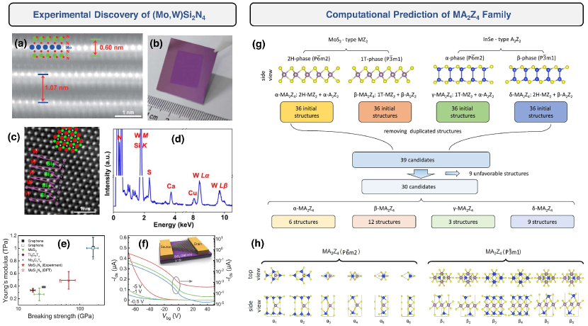
Recently, 2D semiconducting monolayers MoSi2N4 and WSi2N4 have been synthesized experimentally [15] via chemical vapor deposition (CVD) and characterized [see Fig. 1(a)-(d)]. Such monolayers are composed of unstable transition metal nitride cores passivated by two sandwiching Si-N outer-layers. The MoSi2N4 and WSi2N4 monolayers represent an unusual septuple-atomic-layered monolayers that are synthesized exclusively via ‘bottom-up’ approach since they have no 3D counterparts [15]. Importantly, monolayer exhibits excellent mechanical properties, with Young’s modulus (491.4139.1 GPa) and tensile strength (65.818.3 GPa) higher than that of Mxenes and [see Fig. 1(e)]. The optical transmittance of is comparable to that of graphene. Furthermore, can be used as -type channel material for field-effect transistor (FET) -type transistor applications, exhibiting a high on/off ratio of 4000 at 77K [see Fig. 1(f) for the transfer characteristic]. Together with its exceptional ambient stability, optical [16] and excitonic [17] properties, is a promising 2D material for electronics and optoelectronics device applications.
The morphology of MoSi2N4 and WSi2N4 can be generalized into an expansive family of MA2Z4 monolayers. A high throughput computational screening exploring the intercalation of an MoS2-liked MZ2 monolayer in 1T or 2H phase with two InSe-liked A2Z2 outer monolayers in or phase [see Fig. 1(g)] (M = ealy transition metal, alkali-earth metal, VIB element; A = Al, Ga, Si, Ge; Z = S, Se, Te, N, P, As) predicts 72 thermodynamically and dynamically stable monolayers [18]. Structurally, the intercalation morphology of enables four phases (, , , ) with each phase consisting of several substructures [see Fig. 1(h)]. Typically, the , , , structures are the most energetically stable, and their electronic properties can be classified according to the number of valence electrons (i.e. 32, 33 or 34), which gives rise to rich phenomena, such as ferromagnetism, nontrivial band topologies, valleytronic properties and superconductivity [18].
Following the experimental discovery of MoSi2N4 and WSi2N4 monolayers and the computational high-throughput discovery of the broader family, intensive theoretical and computational efforts have been devoted to investigate the physical properties and the potential device application of . As it is impossible for experimental probes to explore the family of , predictive materials modelling via DFT provides a powerful tool to identify that are promising for specific device applications. The proof-of-concept demonstrations of applications, such as transistors [19, 20, 21, 22, 23, 24], contacts [25], photodetectors [26, 27], solar cells [28, 29, 30, 31, 32], photocatalysts [33, 34, 35, 36], luminescence devices [37, 38, 31], thermal management systems [36], battery [39], gas sensors [40, 41] and piezoelectric devices [42], have firmly established as a potential building block of materials for future device technology.
Beyond monolayers, 2D materials can be stacked vertically to form van der Waals heterostructures (vdWHs) [43]. Unlike traditional 3D materials, the absence of dangling bonds on 2D material surfaces allows vertical stacking via weak interlayer van der Waals (vdW) forces, with minimal strain-induced lattice mismatch and interfacial disorder. Such vertical van der Waals (vdW) stacking architecture further enables the use of rotational degree of freedom between layers to engineer the properties unique to vdWHs [44]. vdWHs thus offer a versatile route for synergizing the physical properties of different 2D materials, which enormously expands the design space and functionalities of 2D material devices [45].
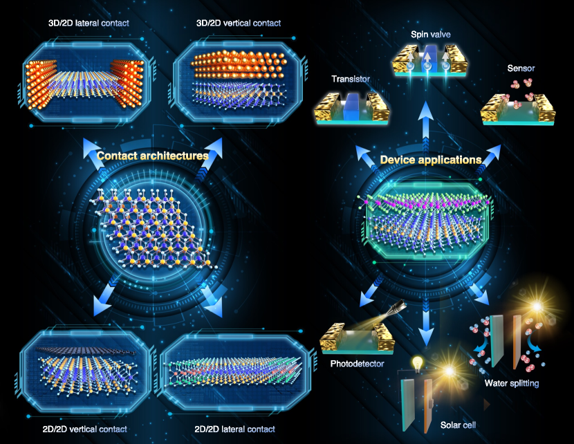
Motivated by the enormous progress made in transition metal dichalcogenide (TMDC)-based vdWHs, -based vdWHs and lateral heterostructures have been extensively studied. In contrast to the monolayer forms of (see Ref. [46] for a recent review of monolayers), -based vdWHs possess greater design challenges due to the enormously large possibilities of material combinations. A bird’s-eye view on the current progress of -based heterostructures, which is needed to tame the enormous design space of -based vdWHs, remains largely incomplete thus far. In this work, we provide a comprehensive review on the theoretical and computational studies of -based heterostructures [see Fig. 2 for an overview of -based heterostructures and their applications]. The physical and interfacial properties of -based vdWHs as well as their potential applications and device performance characteristics are summarized, with specific focus on electronics, optoelectroncis and renewable energy applications. This review aims to provide a summary on the current progress and design challenges of -based vdWHs, and guide the development of novel -based heterostructure device technology.
Outline of this review. This review is presented as followed: Section II provides an overview of MA2Z4 contact heterostructures; Section III discuss the general classification and an overview of MA2Z4-based contacts; Section IV focuses on the physical properties of MA2Z4-based SS vdWH contacts; Section V summarizes the properties of MA2Z4-based heterostructures beyond bilayer vdWHs, such as lateral heterostructures and more complex vdWHs consisting of more than two monolayers; Section IV.3 provides an in-depth discussions on the photocatalytic and photovoltaic abilities of MA2Z4-based SS vdWHs; Section VI provides an outlook on the challenges of MA2Z4-based heterostructures before the conclusion of this review.
II Overview of MA2Z4-based Heterostrutures
The -based heterostructures can be classified, based on the metallic or semiconducting nature of the constituent monolayers, into two main categories: (A) Metal/Semiconductor (MS) vdWHs; and (B) Semiconductor/Semiconductor (SS) vdWHs. For MS vdWHs, two subcategories can be defined: (A1) Ohmic contact in which charge injection can be efficiently achieved without traversing through a potential barrier; and (A2) Schottky contact in which charge injection is significantly impeded by a potential barrier arising from the mismatch of the metal work function and semiconductor band edge energies.
For SS vdWHs, four subcategories arise depending on the relative alignment of the conduction band minimum (CBM) and the valence band maximum (VBM) of the contacting semiconductors: (B1) Type-I vdWHs in which the CBM and VBM originate exclusively from only one of the two contacting semiconductors (straddling band gap); (B2) Type-II vdWHs in which the CBM and VBM are contributed distinctively from two different semiconductors (staggered band gap); (B3) Type-III vdWHs in which the CBM of one semiconductor crosses energetically with the VBM of the other semiconductor (broken band gap), such that this overlapping leads to an overall metallic (or semimetallic) nature of the resulting heterostructure; and (B4) Type-H vdWHs in which the VBM of the heterostructure is contributed by the VBM states of the two different semiconductors (hybridized).
-based heterostructures can be generally constructed via lateral stitching or vertical stacking configurations to form covalently bonded lateral heterostructures or vdWHs, respectively (see Fig. 2). Motivated by the continual discovery of new 2D materials and the advancement of vdW engineering in recent years [47, 48, 49, 50, 51, 52, 53], the physical and chemical properties of -based vdWHs have been intensively studied using DFT simulations in recent years. DFT simulations have predicted a large variety of -based vdWHs having promising application in the areas of optoelectronics [29, 37, 38, 25, 30, 54, 28], in clean energy research pertaining to photocatalysts [35, 34, 33, 29], heat retention [55], and beyond conventional charge transport devices such as spintronics [56] and valleytronics [57]. It should be noted that the Anderson rule, which determines the band alignment of heterostructures solely by aligning the vacuum levels of the constituent materials without considering the interface effects, often yield incorrect predictions of the band alignment [58] due to the omission of interlayer interactions, interfacial charge transfer, interfacial dipole [59], and orbital hybridization [60] that are inevitably present in vdWHs. Explicit direct DFT calculations are thus neccessarily in order to predict the band alignment and contact types of -based heterostructures.
In the following sections, we systematically review the physical properties and the applicaitons of heterostructures based on the contact classifications outlined above. The physical properties of -based contact hetersotructures are summarized in Tables I, II, III, IV.
III Metal/Semiconductor Heterostructures
III.1 -based MS Contacts
Metal/Semiconductor Contact Physics. At the interface of a MS Schottky contact, an energy barrier called Schottky barrier height (SBH) is formed, caused by the difference between the work function of metal and electron affinity (-type Schottky barrier)/ionization potential (-type Schottky barrier) of the semiconductor. Electric current flows across metal and semiconductor components in many modern electronics, therefore the study of SBH formation and its tunability are crucial in mitigating device performance. The SBH can be controlled by appropriately aligning the metal work function with the semiconductor band edge energies according to the Schottky-Mott rule:
| (1a) | |||
| (1b) |
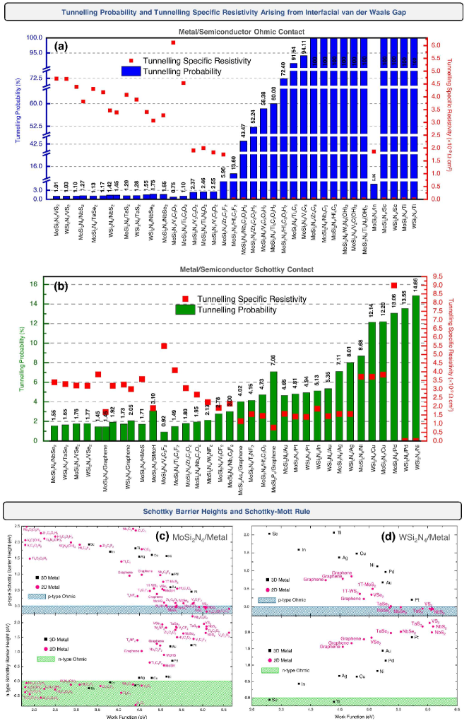
where is the electron/hole SBH, is the electron affinity/ionization potential (or the energies of CBM/VBM relative to vacuum), is the metal work function, and is the slope parameter which characterizes the extend of Fermi level pinning at the interface [71] with denoting the Schottky-Mott limit of a non-interacting MS contact. Most 3D/2D and 3D/3D MS contacts deviate from the Schottky-Mott limit due to the formation of metal-induced gap states (MIGS) and orbital hybridization effects [72]. Such strong interfacial interactions arise due to the presence of many dangling bonds in 3D materials, thus when used as electrode contacts with semiconductor channels, high densities of MIGS can form which pins the Fermi level to a narrow range of values. Monolayer metals, on the other hand, do not have dangling bonds on their surfaces. The absence of MIGS in 2D/2D vdWH metal/semiconductor contact thus suppresses the Fermi level pinning effect [73]. The absence of SH in MS Ohmic contacts provides a low resistance path for charge carriers transport, which is beneficial for energy-efficient device operation [74]. Although SBH is undesirable for electrode applications (such as metal contact to a transistor), they form important functional building blocks for non-reciprocal electronic devices, such as Schottky diodes [75]. Understanding the physics of MS contact formation and the engineering of SBH are thus tremendously important for electronics and optoelectronics applications [71].
For 2D/2D MS contacts, the MIGS and FLP are substantially suppressed due to the weak vdWs coupling between the two constituent monolayers [73]. Nevertheless, substantial deviation of the SBH from the Schottky-Mott rule [Eq. (1)] can still occur due to the formation of interface dipole potential [76] and strain-induced band edge energy shifting [27]. For MoSi2N4 and WSi2N4 – key representative semiconducting monolayers of the MA2Z4 family [15], the MIGS and FLP effects is further suppressed due to two unique aspects: (i) The ‘ultrathick’ morphology of MA2Z4 spatially separates the contacting metal further away from the semiconductor, thus minimizing the wave function penetration of the metallic states into the semiconductor; (ii) The presence of an chemically inert outer Si-N sublayer protects the VBM and CBM states residing in the inner Mo-N (or W-N) corelayer from being hybridized by the contacting metal [77, 78], even for the case where the metal is closely contacted to MoSi2N4 or WSi2N4 monolayers [77]. The combination of these two aspects allows the SBH to be more effectively tuned by appropriate choosing the contacting metal. This aspect is in stark contrast to many other 2D semiconductors such as MoS2 in which the FLP effect is severe, thereby making monolayers attractive candidates for designing MS Ohmic or Schottky contacts.
In addition to SBH, the interfacial potential barrier situated at the vdW gap separated the two contacting monolayers may impede charge ejection efficiency. The charge injection efficiency can be characterized by the tunnelling probability () which is obtained via the Wentzel-Kramers-Brillouin (WKB) approximation, and the tunnelling specific resistivity () via the Simmons formula [79]:
| (2a) | |||
| (2b) |
where , , is the charge of the electron, reduced Planck constant, mass of the electron, respectively, and and are the tunnelling barrier height and width, respectively. Equation 2b is used under intermediate bias voltages, which may give negative unphysical results of its tunnelling current when is too small [77]. The very low voltage approximation of Simmons formula [79] can be used [Equation 3]:
| (3) |
In the following section, we review the SBH, and of MA2Z4-based MS contacts under both 3D/2D and 2D/2D configurations.
Bulk (3D) vs 2D metals. The calculated of MoSi2N4 and WSi2N4-based MS contacts with several representative 3D metals are found to be in the order of [77], which is comparable to low-contact-resistance Bi/MoS2 [80]. In Fig. 3(a), we rank MoSi2N4 and WSi2N4 Ohmic contacts in increasing values of , and also the corresponding . Generally, decreases with increasing since large tunneling probability promotes charge transport across the contact. The is completely absent with = 100% when Sc and Ti are used as 3D metal contacts, thus indicating Sc and Ti as promising candidates for achieving high charge ejection efficiency in MoSi2N4 and WSi2N4. The of 3D/2D MS contacts are generally higher than those of 2D/2D MS contacts due to the stronger coupling between metal and semiconductor in 3D/2D MS contacts [62] [see Fig. 3(b)]. The SBHs of MoSi2N4-and WSi2N4-based 3D/2D and 2D/2D MS contacts are summarized in Figs. 3(c) and (d). 3D metals (In, Sc, Ti) predominantly form -type Ohmic contact, whereas 2D metals () predominantly form -type Ohmic contact.
Recent computational designs of MXene metal contacts to MoSi2N4 reveals that -type Ohmic contacts (e.g. W3N2(OH), V2C(OH)2, Ti4C3) can also be achieved due to the low work function nature such MXenes and the presence of an appropriate interface dipole potential that leads to a proper metal work function alignment with the conduction band continuum of MoSi2N4 [65, 66]. Importantly, the presence of both -and -type Ohmic contacts in MXene/MoSi2N4 heterostructures suggest MXene metal contact can potentially enable the complementary metal-oxide-semiconductor (CMOS) implementation of MoSi2N4 in which both -type and -type devices are needed [81], thus providing a route to greatly expanding the potential usefulness of MoSi2N4-based electronic devices. It should be noted that achieving Ohmic band alignment across a 2D/2D MS contact does not immediately correspond to a low contact resistance. Interfacial tunnelling potential barrier, as discussed above, may still be present due to the vdW coupling nature of the MXene/MA2Z4 contact heterostructure. The tunnelling-specific contact resistivity of MXene/MA2Z4, however, has yet to be catalogued in the literature thus far, and we expect a comprehensive study on the tunneling charge transport to yield important light on the feasibility and performance of MXene/MA2Z4 contacts.
| Materials | Ref. | ||||
|---|---|---|---|---|---|
| Electron | Hole | Electron | Hole | ||
| a0.15 | a0.98 | z0.16 | z1.01 | [37] | |
| z0.213510 | z0.562150 | a0.142057 | a0.063423 | [83] | |
| a9.08 | a9.48 | z15.26 | z9.02 | [38] | |
| z0.273305 | z1.794131 | a0.133276 | a0.179049 | [83] | |
| 1.61951 | 0.1349 | 1.77916 | 0.0657 | [35] | |
| z8.14 | z2.50 | a6.36 | a2.01 | [28] | |
| 0.27 | 1.2 | 0.27 | 1.2 | [15] | |
| 2.32709 | 0.28510 | 2.97531 | 0.26947 | [35] | |
| 0.98376 | 0.10658 | 1.22954 | 0.09998 | [84] | |
| z0.37749 | z0.609322 | a0.37147 | a0.60984 | [85] | |
| z1.73 | z0.172 | a1.721 | a0.174 | [86] | |
| z0.47 | z0.82 | a0.58 | a1.16 | [28] | |
| 4.8832 | 0.0065 | 7.0747 | 0.0065 | [87] | |
| z0.40423 | z0.01047 | a0.3793 | a0.00827 | [85] | |
| z0.48213 | z0.004 | a0.44066 | a0.0028 | [85] | |
| 1.11797 | 0.10649 | 1.28499 | 0.11448 | [84] | |
| z1.732925 | z0.273762 | a1.155009 | a0.266595 | [83] | |
| z2.172 | z0.205 | a2.162 | a0.203 | [86] | |
| z0.826 | z0.085 | a0.125 | a0.075 | [86] | |
| z0.206 | z1.182 | a0.966 | a0.706 | [86] | |
| z1.226 | z1.248 | a1.225 | a1.045 | [86] | |
| z0.386 | z1.874 | a0.446 | a1.476 | [86] | |
| z0.932 | z1.889 | a0.736 | a2.169 | [86] | |
| z0.141 | z1.695 | a10.370 | a0.815 | [86] | |
| z0.093 | z0.076 | a0.25 | a0.694 | [86] | |
| a1.84 | a22.35 | z1.86 | z22.39 | [37] | |
| a1.44 | a24.86 | z2.54 | z43.28 | [38] | |
| 12.67688 | 0.25185 | 12.20292 | 0.23630 | [35] | |
| z1.15 | z3.17 | a0.86 | a2.02 | [28] | |
| 2.06648 | 0.31404 | 2.03585 | 0.29029 | [84] | |
| 58.5223 | 0.0722 | 48.7546 | 0.0746 | [87] | |
| 1.584591 | 25.146891 | 1.187452 | 10.496258 | [83] | |
| 2.342283 | 32.832080 | 2.461746 | 33.032965 | [83] | |
| K→Γ5.555902 | Γ→M0.38638 | - | - | [82] | |
| K→Γ5.85706 | Γ→M0.24851 | - | - | [82] | |
| Γ→M6.04843 | Γ→M0.26266 | - | - | [82] | |
| K→Γ5.63101 | Γ→M0.22369 | - | - | [82] | |
Beyond MoSi2N4 and WSi2N4 monolayers, CrSi2N4 and CrC2N4 from the MA2Z4 family [88] have also been predicted computationally, using DFT and NEGF quantum transport simulations, to exhibit ideal -type Ohmic contacts with Ag and Ti bulk metals at both the vertical MS contact and the lateral contact/channel interface, which are beneficial for achieving high charge injection efficiency across the MS contacts. Figures 3(c) and (d) show the SBH of MS contacts as a function of the metal work function () compiled from the DFT simulation data extracted from previous literature. In general, the two extreme ends of very large and of very small tends to form -type and -type Ohmic contact (or quasi-Ohmic contact with ultralow SBH), respectively, with MoSi2N4 and WSi2N4, due to the alignment of the metal fermi level with the band edges of the semiconducting monolayer. Particularly, 2D Mxenes exhibit a wider range of SBH as compared to bulk metals since the large variety of MXenes broader values [65, 66]. In fact, for the 2D metals that have been investigated so far, MXenes are the only electrode materials predicted to form -type Ohmic contacts with MoSi2N4. As -type and -type contacts are both needed in the implementation of complementary metal-oxide-semiconductor (CMOS) technology which requires both -and -type transistors [89], MXene represents a promising 2D metal family in enabling CMOS functionality in the MA2Z4 family.
We further note that apart being an indispensable structure nearly present in all electronics and optoelectronics devices, MS contacts can also be used as a functional energy conversion device. For example, MoN2/MoSi2N4 can be used as a nanogenerator when MoN2 is dragged along MoSi2N4 in the in-plane direction [42]. An alternating voltage will be induced by the effect of sliding ferroelectricity, which is approximately eight times larger than that of the voltage supplied by a previously studied C/BN nanogenerator.
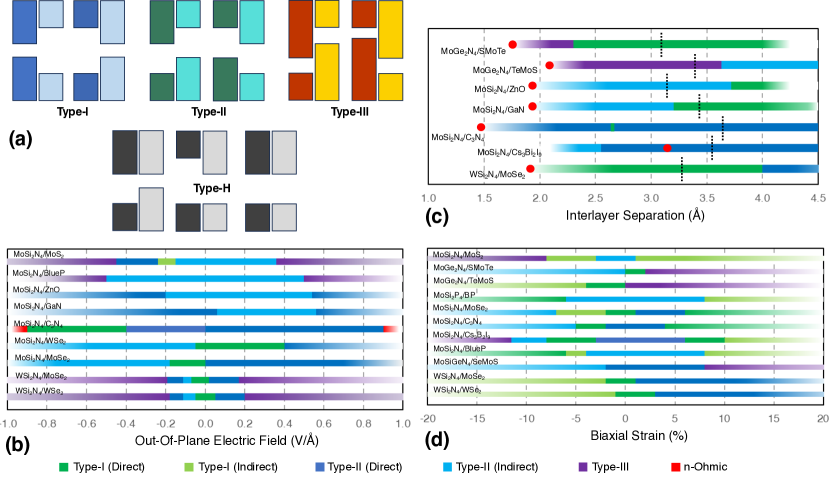
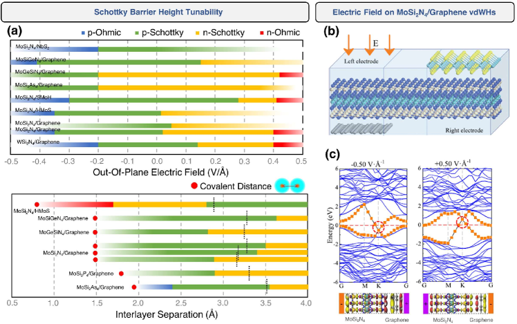
SBH tuning through electric field, strain and Janus phase engineering. A tunable SBH is highly desirable for electronics device applications. Akin to many 2D/2D MS contacts, the MA2Z4-based MS contacts exhibit electric field and strain tunable SBHs. In Fig. 4(a)(Top), we summarize the out-of-plane electric field-tunable SBH of various reported MA2Z4-based MS contacts, and their transitions between Ohmic and Schottky contacts. We define the positive direction of the electric field as pointing from to the contacting metal. We note that forms Ohmic contact as reported in Ref. [77] and Ref. [61], but is reported as a -type Schottky contact with ultra-low -type SBH in Ref. [67]. Such difference arises from different strain and stacking orientation which modifies the electronic bands. Nevertheless, field-tunable SBH is observed in a large variety of MA2Z4-based MS contacts. For example, over the field range of -0.5 to 0.5 V/Å, changes its polarity from -type Ohmic contact to -type Schottky contact. For other MS contacts, a larger positive external electric field can substantially lower the CBM of the semiconducting monolayer to achieve a -type Schottky contact or even -type Ohmic contact. Particularly, /graphene MS contacts exhibit the most versatile field-tunability which transits between various -type Schottky and Ohmic contacts, thus rendering them useful as reconfigurable diode applications [see Fig. 4(b),(c)] [67, 70, 68, 69].
Janus phase engineering provides additional freedom for tuning the SBH heights or even for changing the contact type by reversing the side of the contacting surface. Janus-MoSH when in contact with can form a -type Schottky barrier height of either 0.50 eV or 0.11 eV (ultra-low) by simply reversing the contacting surface of Janus-MoSH [62], whereas Janus-/graphene contact exhibits either an -type or -type Schottky contact depending on its contacting surface [69].
External strain can be used to tune the electronic structures of contact heterostructures [92, 93]. Vertical strain, which modifies mainly the interlayer spacing between the constituent two sub-monolayers, has been widely explored as an efficient tool to tune the SBH and contact types of -based MS Ohmic contacts. Vertical strain can be experimentally achieved through nanomechanical engineering [94], thermal annealing [95], or the insertion of a dielectric between the layers [96]. Figure 4(a)(Bottom) shows the transitions between Ohmic and Schottky contact of 2D/2D MS contacts that are tunable within the vertical compressive/tensile strain range. and are only weakly tunable with vertical strain and retain -type Schottky contact over a large range of vertical strain. , and Janus-MoSiGeN4/graphene, on the other hand, can be tuned between Schottky and Ohmic contacts by varying their interlayer spacings [62, 70, 69, 68]. It should be noted that the interlayer spacings cannot be indefinitely decreased since the contacting atoms could eventually reach the covalent distance to form strongly coupled interfaces. The covalent distance is marked by a red filled circle in Fig. 4(a)(Bottom) which denotes the lower limit of vertical strain tuning.
IV Semiconductor/semiconductor Heterostructures
IV.1 -based Heterostructure Mobility
Carrier mobility enhancement. The mobility of electrons and holes in 2D materials can be significantly enhanced when in heterostructures which stems from either an increased in the in-plane stiffness or a reduction of the effective mass or the deformation potential. Based on the Bardeen-Shockley deformation potential theory (BS-DPT) [97, 98], the carrier mobility due to longitudinal acoustic (LA) phonon scattering in 2D semiconductors can be expressed as:
| (4) |
where , , , , , is the elastic modulus, Boltzmann constant, temperature (taken as about 300 K), effective mass of the carrier in the transport direction, average effective mass of the carrier, deformation potential respectively. High carrier mobility is generally desirable for the construction of transistors [63], photocatalysts [99], excitonic solar cells [100], and many other applications that involve charge current. In transistors application, high carrier mobility directly translates to faster switching speeds and larger current-carrying capabilities, which allows for high speed information processing and greater power output respectively. In solar cell and photocatalytic applications, higher carrier mobility increases the drift and diffusion photocurrent to the collection terminals (in solar cells) or to the oxidation/reduction sites (in photocatalysts) before carrier recombination can take place. Carrier mobility is thus an indispensable quantity for consideration when constructing modern electronics and optoelectronics devices.
Carrier mobility enhancement via vdWH engineering have been investigated for various MA2Z4-based SS contacts, where we summarized the result in Table 1 for the electron and hole mobility of MA2Z4-based SS vdWHs. The carrier mobility of the constituent monolayers are also shown for a comparison. Generally, the carrier mobility of MA2Z4-based SS vdWHs are enhanced when compared to their monolayer counterparts. For instance, [38] and [37] forms Type-I SS vdWH with a significantly larger hole mobility when compared to both the standalone MoSi2N4 and MoSe2. The electron mobility of only in and in MoSi2N4 can be enhanced by an order of magnitude when forming . vdWH engineering thus is an effective method for enhancing carrier mobility.
IV.2 -based SS Contacts
Band alignment. SS vdWHs can be classified into four band alignment types according to the relative position of the building materials’ CBM and VBM. [see Fig. 5(a)]: (i) Type-I, (ii) Type-II, (iii) Type-III, and (iv) Type-H. Type-I materials with direct band gap are useful in light-emitting devices such as diodes and lasers, since the photogenerated carriers easily recombine at the same monolayer. Type-II materials are useful as photocatalysts and solar cells since the photogenerated carriers of opposite polarity can be efficiently separated across different monolayers. Type-III materials are useful for engineering tunneling FET since the electrons from the monolayer with higher energy valence band can occupy the lower energy conduction band of the other monolayer through various tunneling mechanisms. Type-H materials however, are intermediate between Type-I and Type-II, which limits its potential in optoelectronics and photocatalytic applications due to not reaping the full benefits of their distinguishable properties. Type-H materials arised due to hybridization of the out-of-plane orbitals in the vdW gap, and are observed in , , [27] and in vdWHs composed of TMDC monolayers [58, 101].
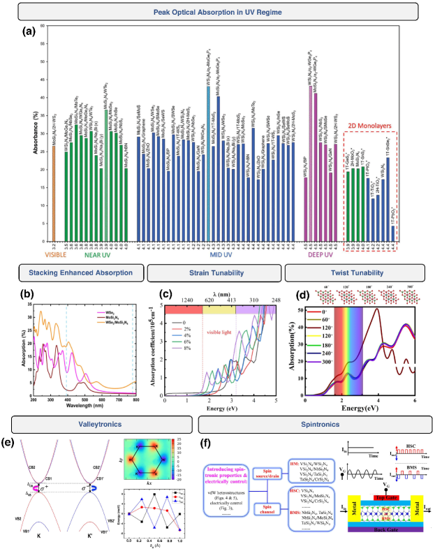
Enhanced optical absorption. Figures 5(b)-(d) shows the band alignment tunability of SS contact vdWHs through the application of out-of-plane electric field and strain (in-plane and vertical). We define the direction of the positive electric field as pointing from to the other semiconductor. The in-plane strain being applied is the biaxial strain () defined as , where and are the strained and unstrained lattice constant respectively. 2D materials are able to withstand a larger strain as compared to 3D materials due to their delayed plastic deformation and fracture phenomena [102]. In the family, has a tensile strength of 50.6 GPa and an in-plane critical strain of 19.5%, making it a suitable material to build vdWHs that show resistance to bond breakage when strain is applied to alter their physical properties. The bandgaps and band edge positions of the SS vdWHs are much more sensitive to biaxial strain than vertical strain [see Figs. 5(c),(d)], rendering the first strain approach useful for constructing optoelectronics that operate in different light absorption regimes. In general, the -based SS contacts show better optical absorption property than their constituent monolayer with absorption peaks at the ultraviolet (UV) regime [see Fig. 6(a),(b)], and the application of strain to manipulate the band alignment can be used to improve their optical absorption spectrum in this regime [see Fig. 6(c) for as a representative material] such as in the case of [83], [83], [37], [33], Janus- [54]. Optical absorption can also be varied based on the stacking orientation of the monolayers, such as in the case of [28] where five different orientations are investigated [see Fig. 6(d)].
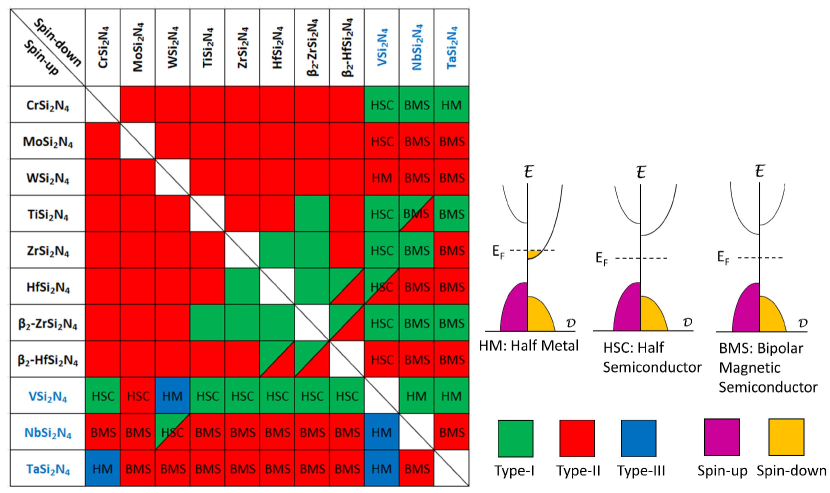
Valleytronics and spintronics. Magnetic semiconducting monolayers can be stacked with other monolayers to form novel vdWHs that have potential applications in valleytronics and spintronics [9]. The broken inversion symmetry of can be exploited when stacked with ferromagnetic to lift the valley degeneracy at the K and K’ valleys through the valley Zeeman effect [57]. Vertical strain can tune the amount of valley splitting thereby demonstrating the potential use of -based magnetic vdWHs for valleytronics devices [see Fig. 6(e)]. Group V-B monolayers , and are magnetic semiconductors due to one unpaired electron in their orbital [56]. vdWHs made from these Group V-B monolayers can be stacked with other monolayers to form half-metals (, , , ), with one spin channel exhibiting Type-III band alignment and the other spin channel having a sizable energy bandgap. on the other hand is a half-semiconductor where the VBM and CBM are contributed from the same spin channel. The realization of half-metals and half-semiconductors through stacking monolayers without the use of external perturbations or chemical modifications, offers a new alternative paradigm in the construction of spintronic devices [see Fig. 6(f)]. The band alignments of various vdWHs based on M = Group IV-B, V-B, VI-B reveals that most of them are potential materials for photodetection (i.e. Type-II band alignment) and for spintronics applications (i.e. spin-polarised metals and semiconductors) [Fig. 7].
Solar-to-hydrogen (STH) efficiency. gas production is a solution towards clean and renewable energy. The solar-to-hydrogen (STH) efficiency which determines the efficiency of hydrogen production from photocatalytic water splitting, is required to be above 10% for the material to be commercially viable [103]. The band edge alignment of (BlueP) results in a high STH efficiency of 21.1%, demonstrating an enhancement over that of monolayer (6.5%) and BlueP (5.1%) [33]. On the other hand, the STH efficiency of which is found to be 9.1%, falls short of the 10% benchmark but is still higher than that of its constituent monolayers [84]. These results show that constructing vdWHs is a suitable approach to improve the photocatalytic capability of the monolayers. In Section IV.3, we discuss in details the photocatalytic properties of MA2Z4 monolayers and SS vdWHs in which the water-splitting performance can be externally tuned via strain and using different pH conditions.
| Metal | Contact Type | Schottky Barrier Height (eV) | Tunnelling Barrier Height (eV) | Tunnelling Barrier Width (Å) | Tunnelling Barrier Probability | Tunnelling Specific Resistivity (10-9 cm2) | Electric Field Tunable? | Vertical Strain Tunable? | Ref. | ||
| n-type | p-type | ||||||||||
| Ohmic | 1.96 | -0.02 | 5.29 | 1.95 | 1.01 | 4.71 | - | - | [61] | ||
| Schottky | 1.94 | 0.53 | 4.40 | 1.88 | 1.76 | 3.20 | - | - | [61] | ||
| Ohmic | 1.87 | -0.04 | 5.21 | 1.93 | 1.10 | 4.39 | - | - | [61] | ||
| Ohmic | 1.65 | -0.03 | 5.14 | 1.88 | 1.27 | 3.82 | - | - | [77] | ||
| Schottky | 0.042 | - | - | - | - | ✗ | ✗ | [67] | |||
| Schottky | 1.63 | 0.09 | 4.74 | 1.87 | 1.55 | 3.39 | - | - | [61] | ||
| Ohmic | 1.86 | -0.03 | 5.12 | 1.91 | 1.2 | 4.08 | - | - | [61] | ||
| Ohmic | 1.86 | -0.03 | 5.14 | 1.93 | 1.13 | 4.31 | - | - | [61] | ||
| Graphene | Schottky | 1.03 | 0.98 | 4.04 | 1.92 | 1.92 | 3.19 | - | - | [61] | |
| Schottky | 1.28 | 0.38 | 4.45 | 1.96 | 1.45 | 3.85 | - | - | [77] | ||
| Schottky | 1.14 | 1.06 | - | - | - | - | ✓ | ✓ | [70] | ||
| Schottky | 0.92 | 0.80 | - | - | - | - | ✓ | ✓ | [67] | ||
| Schottky | 0.68 | 0.97 | 9.98 | 1.3 | 1.45 | 1.67 | ✓ | ✓ | [63] | ||
| HMoS | Schottky | 0.54 | 0.5 | 4.04 | 1.98 | 1.71 | 3.58 | ✓ | ✓ | [62] | |
| SMoH | Schottky | 0.9 | 0.11 | 4.27 | 1.63 | 3.10 | 1.89 | ✓ | ✓ | [62] | |
| Ti4C3 | Ohmic | -0.396 | 1.393 | 0.124 | 0.245 | 91.54 | 1.6 | - | - | [65] | |
| Ti4C3F2 | Schottky | 0.639 | 0.473 | 4.057 | 2.037 | 1.49 | 4.09 | - | - | [65] | |
| Ti4C3O2 | Ohmic | 1.791 | -0.17 | 5.002 | 1.967 | 1.1 | 4.54 | - | - | [65] | |
| Ti4C3O2H2 | Ohmic | -0.446 | 1.483 | 0.684 | 0.603 | 60 | 2.57 | - | - | [65] | |
| V4C3 | Ohmic | -0.151 | 1.779 | 0.106 | 0.182 | 94.11 | 1.25 | - | - | [65] | |
| V4C3F2 | Schottky | 1.445 | 0.1 | 5.015 | 2.044 | 0.92 | 5.49 | - | - | [65] | |
| V4C3O2 | Ohmic | 1.657 | -0.085 | 5.573 | 2.023 | 0.75 | 6.12 | - | - | [65] | |
| V4C3O2H2 | Ohmic | -0.375 | 1.913 | 0.637 | 0.68 | 58.38 | 2.79 | - | - | [65] | |
| Zr4C3 | Ohmic | -0.813 | 2.366 | 0 | 0 | 100 | 0 | - | - | [65] | |
| Zr4C3F2 | Ohmic | -0.164 | 1.879 | 2.866 | 1.626 | 5.96 | 1.75 | - | - | [65] | |
| Zr4C3O2 | Schottky | 1.753 | 0.098 | 4.511 | 1.847 | 1.8 | 3.05 | - | - | [65] | |
| Zr4C3O2H2 | Ohmic | -0.561 | 2.281 | 0.716 | 0.749 | 52.24 | 3.58 | - | - | [65] | |
| Nb4C3 | Ohmic | -0.109 | 2.418 | 0 | 0 | 100 | 0 | - | - | [65] | |
| Nb4C3F2 | Schottky | 1.217 | 0.97 | 3.901 | 1.733 | 3 | 2.16 | - | - | [65] | |
| Nb4C3O2 | Schottky | 2.217 | 0.075 | 4.723 | 1.768 | 1.95 | 2.68 | - | - | [65] | |
| Nb4C3O2H2 | Ohmic | -0.065 | 2.489 | 0.902 | 0.856 | 43.47 | 4.38 | - | - | [65] | |
| Hf4C3 | Ohmic | -0.915 | 2.711 | 0 | 0 | 100 | 0 | - | - | [65] | |
| Hf4C3F2 | Ohmic | -0.118 | 1.921 | 2.304 | 1.283 | 13.6 | 1.31 | - | - | [65] | |
| Hf4C3O2 | Schottky | 1.5 | 0.5453 | 3.981 | 1.493 | 4.73 | 1.45 | - | - | [65] | |
| Hf4C3O2H2 | Ohmic | -0.284 | 2.174 | 0.419 | 0.487 | 72.4 | 2.19 | - | - | [65] | |
| T2NF2 | Schottky | 1.4 | 0.31 | 4.12 | 1.53 | 4.15 | 1.55 | - | - | [66] | |
| W2NF2 | Schottky | 1.83 | 0.02 | 5.18 | 1.65 | 2.13 | 2.24 | - | - | [66] | |
| V2CF2 | Schottky | 1.83 | 0.02 | 4.72 | 1.61 | 2.78 | 1.91 | - | - | [66] | |
| V3C2O2 | Ohmic | 1.92 | -0.2 | 5.48 | 1.56 | 2.37 | 1.91 | - | - | [66] | |
| V4C3O2 | Ohmic | 1.79 | -0.1 | 5.34 | 1.55 | 2.55 | 1.83 | - | - | [66] | |
| Ti4N3O2 | Ohmic | 1.76 | -0.03 | 5.04 | 1.61 | 2.46 | 2 | - | - | [66] | |
| W3N2(OH)2 | Ohmic | -0.12 | 1.99 | 0 | 0 | 100 | 0 | - | - | [66] | |
| V2C(OH)2 | Ohmic | -0.2 | 2.06 | 0 | 0 | 100 | 0 | - | - | [66] | |
| Ti4N3(OH)2 | Ohmic | -0.26 | 2.11 | 0 | 0 | 100 | 0 | - | - | [66] | |
| Ohmic | 2.29 | -0.05 | 5.19 | 1.96 | 1.03 | 4.70 | - | - | [61] | ||
| Schottky | 1.84 | 0.34 | 4.39 | 1.88 | 1.77 | 3.19 | - | - | [61] | ||
| Ohmic | 2.18 | -0.06 | 5.12 | 1.92 | 1.17 | 4.18 | - | - | [61] | ||
| Ohmic | 2.00 | -0.04 | 5.04 | 1.84 | 1.45 | 3.39 | - | - | [77] | ||
| Ohmic | 2.02 | -0.01 | 4.68 | 1.88 | 1.55 | 3.41 | - | - | [61] | ||
| Ohmic | 2.18 | -0.05 | 5.02 | 1.90 | 1.28 | 3.89 | - | - | [61] | ||
| Schottky | 1.98 | 0.02 | 4.60 | 1.87 | 1.65 | 3.28 | - | - | [61] | ||
| Graphene | Schottky | 1.56 | 0.78 | 4.04 | 1.89 | 2.05 | 3.00 | - | - | [61] | |
| Schottky | 1.79 | 0.22 | 4.39 | 1.89 | 1.73 | 3.26 | - | - | [77] | ||
| Schottky | 1.67 | 0.85 | 0 | 0 | 100 | 0 | ✓ | ✗ | [64] | ||
| Graphene | Schottky | 0.63 | 1.13 | - | - | - | - | ✓ | ✓ | [68] | |
| Graphene | Schottky | 1.03 | 0.74 | - | - | - | - | ✓ | ✓ | [68] | |
| Graphene | Schottky | 0.13 | 0.60 | 6.11 | 1.04 | 7.08 | 0.77 | ✓ | ✓ | [63] | |
| Graphene | Schottky | 0.32 | 0.31 | 5.67 | 1.31 | 4.02 | 1.14 | ✓ | ✓ | [63] | |
| Graphene | Schottky | 0.03 | 0.45 | 4.35 | 1.89 | 1.77 | 3.226 | - | - | [88] | |
| Graphene | Schottky | 0.05 | 1.85 | 4.08 | 1.69 | 3.02 | 2.046 | - | - | [88] | |
| Metal | Contact Type | Schottky Barrier Height (eV) | Tunnelling Barrier Height (eV) | Tunnelling Barrier Width (Å) | Tunnelling Barrier Probability | Tunnelling Specific Resistivity (10-9 cm2) | Ref. | ||
| n-type | p-type | ||||||||
| Sc | Ohmic | -0.06 | 2.03 | 0 | 0 | 100 | 0 | [77] | |
| Ti | Ohmic | -0.12 | 2.06 | 0 | 0 | 100 | 0 | [77] | |
| Ni | Schottky | 0.82 | 1.13 | 2.08 | 1.29 | 14.86 | 1.27 | [77] | |
| Cu | Schottky | 0.65 | 1.48 | 2.80 | 1.23 | 12.14 | 3.71 | [77] | |
| Pd | Schottky | 1.14 | 0.97 | 2.98 | 1.13 | 13.55 | 1.02 | [77] | |
| Ag | Schottky | 0.67 | 1.37 | 3.01 | 1.42 | 8.01 | 1.56 | [77] | |
| In | Schottky | 0.43 | 1.59 | 2.94 | 1.69 | 5.13 | 1.86 | [77] | |
| Pt | Schottky | 1.85 | 0.20 | 4.04 | 1.46 | 4.94 | 1.39 | [77] | |
| Au | Schottky | 1.44 | 0.68 | 3,73 | 1.48 | 5.35 | 1.43 | [77] | |
| Ag | Ohmic | -0.03 | 0.54 | 2.91 | 1.3 | 10.45 | 1.954 | [88] | |
| Au | Schottky | 0.02 | 0.54 | 3.69 | 1.44 | 5.86 | 1.372 | [88] | |
| Cu | Ohmic | -0.03 | 0.52 | 2.79 | 1.09 | 15.48 | 8.9 | [88] | |
| Ni | Ohmic | -0.01 | 0.6 | 3.17 | 1.2 | 11.27 | 2.205 | [88] | |
| Pd | Ohmic | -0.02 | 0.74 | 2 | 0.8 | 31.42 | 3.81 | [88] | |
| Pt | Ohmic | -0.01 | 0.75 | 2.99 | 1.08 | 14.76 | 8.93 | [88] | |
| Ti | Ohmic | -0.04 | 0.58 | 2.04 | 1.03 | 22.21 | 6.87 | [88] | |
| Ag | Schottky | 0.07 | 1.84 | 3.52 | 1.51 | 5.55 | 1.499 | [88] | |
| Au | Schottky | 0.32 | 1.54 | 4.1 | 1.55 | 4.01 | 1.601 | [88] | |
| Cu | Ohmic | -0.06 | 1.79 | 1.24 | 0.6 | 50.48 | 2.3 | [88] | |
| Ni | Schottky | 0.15 | 1.81 | 0.32 | 0.13 | 88.74 | 5.23 | [88] | |
| Pd | Schottky | 0.14 | 1.81 | 3.64 | 1.3 | 7.84 | 1.294 | [88] | |
| Pt | Schottky | 0.19 | 1.73 | 3.69 | 1.22 | 9.07 | 1.340 | [88] | |
| Ti | Ohmic | -0.13 | 1.75 | 0 | 0 | 100 | 0 | [88] | |
| Semiconductor | Alignment Type | Bandgap (eV) | Bandgap Tunability | Optical Absorption Peaks | Application | Ref. | ||||
| Magnitude | Direct / Indirect | Electric Field | Vertical Strain | Biaxial Strain | ||||||
| Type-II | 1.26 (PBE), 1.84 (HSE) | Indirect | - | - | - | UV | Optoelectronics | [32] | ||
| Type-II | 1.12 (PBE) | Indirect | ✓ | - | ✓ | UV | Optoelectronics | [90] | ||
| Type-II | 1.93 (HSE) | Indirect | - | - | - | UV | H2O Photocatalyst | [104] | ||
| Type-I | 1.39 (PBE), 1.82 (HSE) | Direct | ✓ | - | ✓ | Visible, UV | FET, Optoelectronics | [37] | ||
| Type-I | 1.17 (PBE), 1.57 (HSE) | Direct | ✓ | - | - | Visible, UV | FET, Photovoltaic | [38] | ||
| Type-II | 1.38(PBE),1.81(HSE) | Indirect | - | - | - | Visible, UV | H2O Photocatalyst | [105] | ||
| InSe | Type-II | 1.35 (PBE), 1.61 (HSE) | Direct | - | - | - | UV | Photocatalyst | [35] | |
| ZnO | Type-II | 1.60 (PBE) | Indirect | ✓ | ✓ | - | - | Optoelectronics | [31] | |
| GaN | Type-I | 1.56 (PBE) | Direct | ✓ | ✓ | - | - | Optoelectronics | [31] | |
| Type-II | 1.74 (HSE) | Direct | - | - | - | Visible, UV | Photocatalyst | [34] | ||
| Type-II | 1.86 (PBE), 2.66 (HSE) | Direct | ✓ | ✓ | ✓ | Visible, UV | Optoelectronics | [30] | ||
| Type-II | , | Indirect | - | ✓ | - | - | Valleytronics | [57] | ||
| Type-II | 0.91 (PBE) | Direct | - | ✓ | ✓ | Visible, UV | Optoelectronics | |||
| Photocatalyst | [29] | |||||||||
| BlueP | Type-II | 1.13 (PBE), 2.02 (HSE) | Indirect | ✓ | - | ✓ | Visible, UV | FET, Optoelectronics | [91] | |
| Type-II | 1.18(PBE), 2.00(HSE) | Indirect | - | - | ✓ | Visible, UV | Photocatalyst | [33] | ||
| Type-II | 0.93 (PBE), 1.52 (HSE) | Indirect | - | ✓ | ✓ | Visible, UV | Photocatalyst | [106] | ||
| SeMoS | Type-I | 1.55 (HSE) | Indirect | - | - | - | Visible, UV | Optoelectronics | [104] | |
| Type-II | 1.70 (PBE), 2.15(HSE) | Indirect | - | - | - | Visible, UV | Photocatalyst | [84] | ||
| MoS2 | Type-II | 2.08 (HSE) | Indirect | - | - | - | UV | H2O Photocatalyst | [104] | |
| SeMoS | Type-II | 1.26 (HSE) | Indirect | - | - | - | Visible, UV | H2O Photocatalyst | [104] | |
| SMoTe | Type-I | 0.27 (PBE) | Direct | - | ✓ | ✓ | Visible, UV | Optoelectronics | [54] | |
| TeMoS | Type-III | 0 (PBE) | NA | - | ✓ | ✓ | Visible, UV | Optoelectronics | [54] | |
| BP | Type-II | 1.02 (HSE) | Direct | - | - | - | Visible, UV | Photovoltaic | [28] | |
| SeMoS | Type-II | 0.87 (PBE),1.28 (HSE) | Direct | - | ✓ | ✓ | Visible | Photovoltaic | [82] | |
| Infrared | ||||||||||
| MoSe2 | Type-II | 1.26 (PBE) | Direct | ✓ | ✓ | ✓ | Visible, UV | Optoelectronics | [83] | |
| WSe2 | Type-II | 1.16 (PBE) | Direct | ✓ | ✗ | ✓ | Visible, UV | Optoelectronics | [83] | |
IV.3 Photocatalyst & Solar Energy Conversion
IV.3.1 Photocatalytic water splitting
Photocatalytic water splitting (PCWS) is an effective way to solve the problem of energy crisis and environmental pollution. PCWS usually consists of the following steps [3, 107]: (1) Photons with energy larger than the photocatalyst’s bandgap excite electrons from its valence bands to conduction bands, generating electron-hole pairs; (2) photogenerated carriers diffuse or drift to the surfaces of the photocatalyst; and (3) photogenerated electrons participate in the hydrogen evolution reaction (HER) to generate hydrogen, whereas photogenerated holes participate in the oxygen evolution reaction (OER) to generate oxygen. The conventional PCWS photocatalyst should meet the following requirements to enable the two half-reactions to happen simultaneously [108, 109]: (i) photocatalyst having an appropriate bandgap to obtain sufficient light harvesting; (ii) band edge positions of photocatalyst should span the redox potential levels; and (iii) the photogenerated carriers should provide sufficient driving force to overcome the energy barriers in HER and OER processes, i.e. the potentials between the photocatalyst’s CBM and the reduction level must be large enough to provide strong reduction ability, while the potential between photocatalyst’s VBM and the oxidation level should be large enough to provide strong oxidation ability. 2D photocatalysts have drawn extensive attentions as they exhibit obvious advantages in improving the photocatalytic activities [110, 111], such as tuning their bandgaps through altering the thickness, introducing atomic defects, or applying strain. The ultrathin thickness of 2D materials could also shorten the photogenerated carriers’ migration distances, and their planar structures with high specific surface areas can provide more active sites and offer ideal platforms for combining with other co-catalysts.
The tunability of the bandgap of family for use as photocatalysts motivates further exploration of their potential PCWS ability. By exploring the electronic and photocatalytic features of (M = Cr, Mo, W; A = Si, Ge; Z = N, P) monolayers, Mortazavi [36] found that the and monolayers possess suitable band edge positions, high electron and hole mobility, and strong visible light harvesting ability, which makes these monolayers highly promising candidates for PCWS applications. By screening 54 kinds of possible combinations of family, Chen have confirmed that only and under feasible biaxial tensile strain possess the ability for overall PCWS [see Fig. 8] [112]. Theoretical study by Jian [113] reported that pristine and compressive are promising PCWS photocatalysts having excellent solar energy absorption abilities for water oxidation and reduction. Particularly, compressive strain leads to the spatial separation of photoexcited electrons and holes, which is favorable for enhancing their separation rates. Rehman explored the electronic and photocatalytic properties of (M = Cr, Mo, W) monolayers based on bandgap center [114]. These three monolayers possess sufficient kinetic potentials to drive both water redox reactions, with in-plane compressive strains found to enhance the overall PCWS of all these monolayers. However, pristine and biaxially strained is more favourable for PCWS application due to its strong absorption in the visible regime as compared to and which have strong absorption ability only in the ultraviolet regime. Ren evaluated the HER performances of MX2Y4 monolayers (M = Cr, Hf, Mo, Ti, W, Zr; X = Si, Ge; Y = N, P, As) and their mechanical properties, unearthing TiSi2N4 and ZrSi2N4 as highly efficient HER catalysts due to the small change in Gibbs free energy during adsorption [86].
By using high-throughput screening, Lin unearthed 35 -based monolayers with appropriate bandgap and suitable band edge positions from 648 candidates [115]. After further analysis of the structural stability, free energy change in OER, exciton property, and carrier mobility, - and - have been chosen as highly efficient OER photocatalysts. The bandgaps of monolayers are found to primarily dependent on their M-Z bonding strength and electron distribution, while their OER activities are closely related to the adsorption ability of the O atom on the reaction site. It is worthwhile to note that the potential of MA2Z4 family for CO2 reduction has also been investigated, such as the lateral . High-throughput screening on 104 types of Janus-MA2Z4 monolayers has uncovered and as efficient CO2 photocatalysts in the visible regime [116].
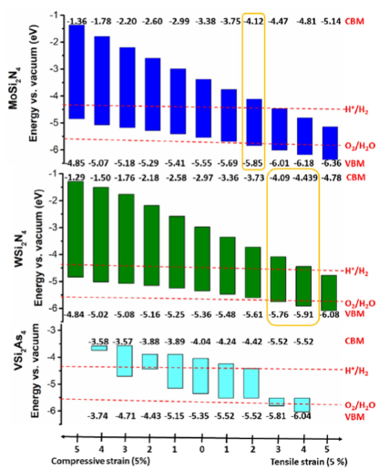
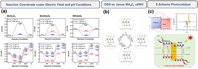
Role of electric field in PCWS. Recently, PCWS reactions based on Janus 2D materials have been proposed [117, 103]. The intrinsic electric field in Janus 2D materials not only promotes the spatial separation of electrons and holes but also breaks the conventional bandgap (1.23 eV) restriction required of PCWS. This enables the harvesting of photons with frequencies below the visible regime for PCWS. Inspired by the first synthesis of Janus-MoSSe, the photocatalytic performance of other Janus materials have been explored [118, 119, 120, 121]. Yu predicted the excellent stability of Janus- and Janus- monolayers for PCWS reactions, in which both of these two monolayers are semiconductors that have indirect bandgaps, suitable band edge positions, excellent optical absorption ability, and large carrier mobility anisotropy [85]. The intrinsic electric fields induced by these Janus structures not only boost the spatial separation of photogenerated carriers, but also provides a potential offset at the HER and OER catalytic sites which enables the photogenerated carriers to provide additional driving force to lower the Gibbs free energy in the redox reactions [see Fig. 9(a)]. Additionally, introducing N atom vacancies to the surface effectively lowers the HER and OER overpotentials. When pH is 3 or , the overall redox processes could proceed simultaneously and spontaneously on the surfaces of Janus- and Janus- under light irradiation [see Fig. 9(b) for a schematic of OER reaction taking place on Janus-]. Lv investigated the structure, electronic property, and carrier mobility of various stacking configurations of bilayer Janus- [87]. The dipole moment formed across the structure plays a big part in modulating the bandgaps through creating a built-in electric field, which causes a shift in the energy bands of each monolayer to achieve Type-II alignment. Additionally, the carrier mobility of bilayer Janus- () is enahcned by one order of magnitude compared to its monolayer form (), thus revealing Janus- as a multifunctional 2D materials that also has potential use in electronics device applications.
PCWS based on MA2Z4 vdWHs. The construction of vdWHs offer another effective avenue to design highly efficient PCWS catalysts [122, 123]. Based on the charge transfer path, the mechanism of PCWS catalysts in vdWHs can usually be divided into either Type-II or Z-scheme [124]. Since the first successful synthesis of , some -based Type-II and Z-scheme vdWH photocatalysts are proposed. Zeng reported the good thermodynamic stability and potential PCWS application of [34] which has efficient charge carrier separation at the interface and excellent optical absorption in the visible regime. Moreover the absolute value of its free energy in hydrogen adsorption is very close to zero. The thus exhibits excellent HER ability for gas generation. In addition, other -based vdWHs such as [105], [37], [106], [35], [84] are predicted to be potential vertical PCWS catalysts.
(BlueP) vdWH has potential in PCWS due to its Type-II band alignment [33]. There are three possible photoinduced carrier transfer paths in [see Fig. 9(c)(Top Left)]: (Path-I) electrons transfer from the ’s conduction bands to the BlueP’s valence bands and the ’s valence bands, (Path-II) electrons and holes recombine with each other between the BlueP’s conduction bands and the ’s valence bands, and (Path-III) electrons transfer from ’s conduction bands to the BlueP’s valence bands. The presence of a built-in electric field created by the interface dipole [see Fig. 9(c)(Top Right)] leads to the suppression of charge recombination through Path-I and Path-III. When the charges recombine along Path-II, the excess electrons at the ’s conduction bands participate in the HER and the excess holes at the BlueP’s valence bands participates in the OER [see Fig. 9(c)(Bottom)]. The energy difference between ’s CBM and HER potential, and the energy difference between BlueP’s VBM and OER potential at pH = 0, are 0.71 and 0.81 eV, respectively. These values are higher than the assumed energy loss in carrier migration of 0.2 in HER and 0.6 eV in OER [103], implying that vdWH has both good reduction and oxidation ability. Moreover, its light absorption performance could be further improved by applying tensile strain in the range of 0 to 8%. These findings show that vdWH is a promising Z-scheme PCWS catalyst. Huang theoretically screened 4 configurations of Janus- vdWHs as highly efficient Z-scheme PCWS catalysts from a total of 12 stacking configurations [125]. This suggests that stacking configurations and twist engineering [126] can potentially be used to further optimize the PCWS capabilities of MA2Z4 heterostructures. (X = S, Se) has been studied for their HER ability with the introduction of vacancy defects, showing that these vdWHs are Z-scheme PCWS photocatalysts, and S/Se vacancies are able to provide the most favourable vacant sites for the H atom to undergo HER at pH = 0 [104].
IV.3.2 Solar-to-electricity energy conversion
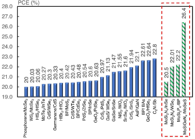
-based heterostructures have attracted much attention in solar cell applications due to the generally good spatial separation of photogenerated carriers in vdWHs [135]. For example, vdWH [28] has can effectively separate the photogenerated carriers due to its Type-II. The hole carrier mobility and optical absorption ability of are improved as compared to its constituent monolayers. Moreover, the predicted solar-to-electricity power conversion efficiency (PCE) based on an excitonic solar cell setup reaches 22.2%, which is comparable to other high-performance (PCE 15%) vdWHs obtained through high-throughput screening [127] and in several other works [130, 131, 132, 133, 134, 129, 27]. Janus-MoSSe/MoGeSiN4 is found to have multiple strain-tunable absorption peaks in the visible and infrared regime, and exhibits high PCE value of 27% through changing its interlayer distance and biaxial strain [82]. and are also potential candidates for excitonic solar cell with PCE of 20.5% and 22.0%, respectively. Fig. 10 shows the reported PCE values of MA2Z4-based vdWHs benchmarked against other high solar-to-electricity performance vdWHs that are potential candidates for constructing excitonic solar cells. We note that solar cell efficiency well over 20% has been achieved in other materials, such as crystalline silicon and perovskite [136, 137, 138]. The MA2Z4 heterostructure-based solar cell has several potential advantageous over bulk semiconductor and perovskites. For instance, vdWH engineering of MA2Z4 and other 2D materials can be used to broaden the absorption spectral range while still retaining their ultracompact device geometry, an aspect difficult to achieve using bulk semiconductors. The excellent ambient stability of MA2Z4 is also more advantageous than other nanomaterial-based solar cell, such as perovskites and organic solar cells [139], which are faced with long-term stability issues.
In heterostructure, a direct bandgap semiconductor with Type-II band alignment, possesses strong visible light absorption [30]. The band alignments could be switched between Type-I and Type-II by using external electric field, modulation of interlayer spacing, and in-plane strain [see Fig. 5(b)-(d)] which renders a promising candidate as a tunable optoelectronic materials. The contact type of can also be tuned by the same methods and a photodetector based on the vdWH has been proposed, which exhibits an enahcned the photocurrent when a tensile strain is applied across the device [90], suggesting potential coupled opto-electro-mechanical applications [140]. Other -based vdWHs [see Fig. 5(b)-(d)] have also been shown to possess tunable band alignment such as [29], [38], [31], [31] and Janus- [54].
V Heterostructures beyond vertical stacking
V.1 Trilayered Vertical Heterostructures
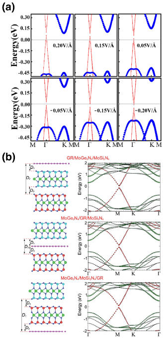
We now review the computational studies of -based multilayered vdWHs beyond bilayer morphology. Bandgap engineering of graphene can be achieved in a triple-layered structure of in which a small bandgap of either 47 meV or 39 meV in the Dirac point of graphene, depending on the stacking configuration, can be generated [69]. Interestingly, external electric field can induce transitions of the contact types between Schottky and Ohmic contact as shown in Fig. 11(a). Apart from using different monolayer combinations, the stacking sequence of graphene and MA2Z4 can also be used to engineer the bandgap and overal contact types of the trilayered-heterostructures. When combining graphene with and [25] to form the trilayered-heterostructures of , and , the bandgap of can be reduced and small band gap of (17-46) meV can be opened at the Dirac point of graphene [see Fig. 11(b)]. Importantly, the /-type Schottky barrier height between graphene with bilayer for all three contact positions, are lower than that obtained for graphene contacting with and monolayer [141], thus showing that stacking sequence beyond bilayer morphology can be harnessed to effectively tune the electronic and contact properties of vdWHs.
V.2 Lateral Heterostructure
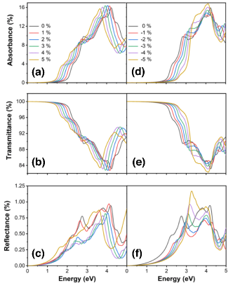
Besides -based vdWHs, -based lateral heterostructures have also been studied recently. To avoid structural instability, covalently bonded lateral heterostructures require small structural mismatch at the contacting interface due to the presence of edge dangling bonds that has to approach each other at appropriate angles. An edge contact transistor based on contacting with 3D Au electrodes reveals that low SBH can be obtained for three different configurations that benefits electrons injection between Au and [142]. The metallic members of MA2Z4 family, such as TaSi2N4 and NbSi2N4 can also be used as lateral edge contacts to MoSi2N4 and WSi2N4 semiconducting channels [143]. Interestingly, the metallic TaSi2N4 and NbSi2N4 are akin to highly -doped MoSi2N4 and WSi2N4 with heavy substitution of Mo and W atoms by Ta and Nb atoms. Because of the narrow-band nature [144] of metallic TaSi2N4 and NbSi2N4 monolayers around the Fermi level, such edge-type electrodes serve as cold source contacts [145] that are highly beneficial for achieving steep-slope transistor operation. The ultralow subthermionic 10 to 30 mV/decade subthreshold swing achieved in a 12-nm FETs composed of lateral heterostructure Si2N4/Si2S4 (where = Mo, W; and = Ta, Nb) [143] suggest the potential usefulness of MA2Z4 MS lateral heterostructures for constructing electronic devices with ultralow power consumption. Laterally stitched and exhibits strain-tunable optical properties with strong absorbance in the visible light regime [see Fig. 12(a)-(f)], thus further suggesting their potential usage in solar cell applications [146].
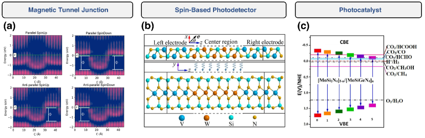
forms a magnetic tunnelling junction (MTJ) with a tunnelling magnetoresistance (TMR) mechanism based on the half-metallicity of [147]. is a ferromagnetic half-metal with Curie temperature of 500 K which is higher than that of other magnetic 2D monolayers, such as and (about 50 K). Thus, is potentially useful for spintronic applications at room temperature. Under a biased voltage range of 100 mV, the TMR which is defined as where is the charge current across the parallel/anti-parallel polarization between the ferromagnets, is about seven orders of magnitude larger than the previously studied heterostructure [148]. Under the same range of bias voltage, the spin injection efficiency, defined as where is the up/down polarization of the spin current, is almost 100% [see Fig. 13(a) for the local spin density of states along the device’s transport direction]. Quantum transport simulation shows that the photocurrent of [see Fig. 13(b) for the device structure] is dependent on the incident and polarization angle [26]. Using appropriate photon energies and polarization angles, the spin-filter and spin-valve effects can be generated, rendering the heterostructure a potential usage as a spin-based photodetector.
For electrochemical applications, [149] lateral heterostructure can be used as a photocatalyst for reduction [see Fig. 13(c)]. Changing the chemical composition of the structure via can effectively tune its optical and photocatalytic properties. In particular, exhibits the highest absorption in the visible regime and has the lowest activation energy for reduction. thus offers a promising platform for developing novel sustainable technology.
VI Prospects and Outlooks of MA2Z4 Heterostructures
Recent advances on the computational design of heterostructures, as reviewed in the previous sections, suggest the potential and strengths of heterostructures in electronics, optoelectronics and renewable energy applications. In this Section, we first provide a concise summary to contrast the strengths of MA2Z4-based heterostructures as compared with other commonly studied 2D materials. This is then followed by a discussion on the prospects and outlooks on the design of MA2Z4 heterostructures moving forward. Recommendations on future research based on emerging computational design techniques, such as data-driven design and computational simulations of the experimental growth of MA2Z4 heterostructures, are presented.
VI.1 Comparing MA2Z4 heterostructures with other 2D material heterostructures: Strengths and opportunities
Metal/semiconductor contact interface. Metal-induced gapped states and metallization effect are considerably weaker at the contact interface in MoSi2N4 and WSi2N4-based MS contacts when compared to other 2D semiconductors such as MoS2 in which severe metallization is a commonplace [150]. Such distinctive behavior arises from the outer Si-N sublayer which acts as a built-in protection layers that protect the band edge electronics states, which predominantly localized in the inner Mo-N core-layer [77]. As the band edges states are well ‘insulated’ from the external contacting metals, the Fermi level pinning effect is substantially weaker, even when contacted by 3D bulk metals that are known to substantially metalize 2D TMDCs, than many other 2D semiconductors. The suppression of the Fermi level pinning effect also suggest that the SBH in MoSi2N4 and WSi2N4 MS contacts can be more flexibility engineered via contacting metal electrodes of different Fermi level.
We further note that the unusual built-in sublayer protection – a distinctive feature not found in TMDC and many other 2D semiconductors such as phosphorene and InSe – has only been characterized and discussed in MoSi2N4 and WSi2N4 [77, 61]. Whether such behavior is a general feature universal to the MA2Z4 family remains a question that is still open for computational investigation. In terms of experimental investigations, transport measurements should be carried out using different work function metals to determine the pinning factors, metal evaporation rates, degree of surface damage and resist residue, and transferred versus deposited contacts. Transfer length method (TLM) and four-point measurements are expected to be useful in determining the contact resistances, which should also be measured at different temperatures to determine the carrier injection mechanisms. We highlight that TLM design should include both short-and long-channel devices, so to separately investigate the contact-limited and the channel-limited transport mechanisms, respectively.
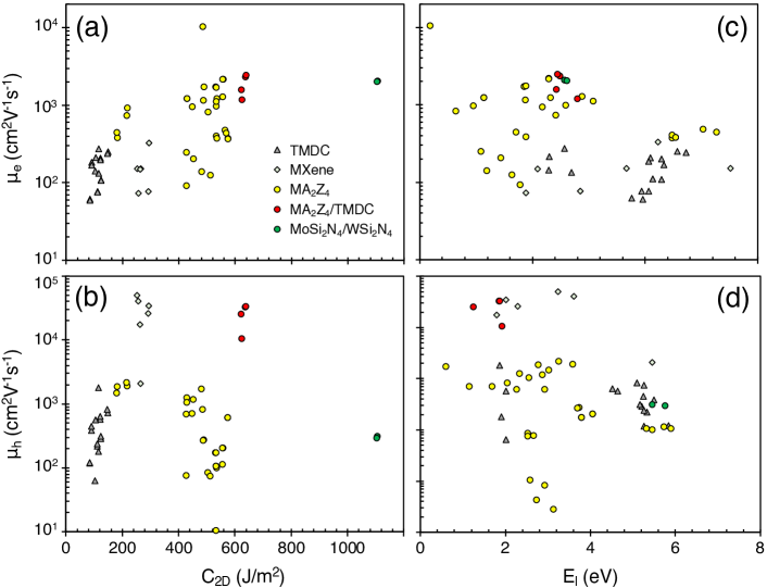
Carrier mobility. Several semiconducting MA2Z4 monolayers, such as the MoSi2N4, WSi2N4, MoGe2N4 and the Janus subfamily of MoSiGeN4, exhibits higher carrier mobility than TMDC monolayers (see Table I). According to the Bardeen Shockley deformation potential theory (BS-DPT) (see Eq. 4), the carrier mobility is proportional to the elastic modulus . In Fig. 14, we examine the correlations between the carrier mobility with elastic modulus and deformation potential, for five representative classes of: (i) TMDC monolayers (MX2 where M = Mo, W and X); (ii) MXene (MCO2 where M = Hf, Ti, Zr); (iii) MA2Z4 monolayers (MoSi2N4, WSi2N4, CrSi2N4, HfSi2N4, ZrSi2N4, TiSi2N4, MoGe2N4, MoSi2As4, MoSi2P4, MoSiGeN4, WSiGeN4); (iv) MA2Z4/TMDC heterostructures (WSi2N4/MoSe2, WSi2N4/WSe2); and (v) MoSi2N4/WSi2N4 heterostructure. Generally, the electron mobility of MA2Z4 monolayers are higher than that of the other 2D semiconductors [Fig. 14(a)]. Interestingly, the higher electron mobility can be well correlated with their high elastic modulus which arises from their thicker lattice where larger force is required to deform the lattice [153, 87]. The thus provides a good single descriptor of higher electron carrier mobility in MA2Z4 monolayers and heterostructures. In contrast, the hole mobility does not strongly correlate with [Fig. 14(b)] as the hole mobility is influenced by a more complex interplay between , and the carrier effective masses. For the deformation potential, higher electron and hole mobility can generally be observed in MA2Z4 and their heterostructures with lower [Figs. 14(c) and 14(d)], which arises from the relation of according to the BS-DPT in Eq. (4).
The excellent mechanical properties of MA2Z4 provides another avenue to engineer their carrier mobility. The MA2Z4 family members, such as MoSi2N4 and WSi2N4 , have exceptionally high Young’s modulus and mechanical breaking strength [15, 154] (i.e. 479 and 49 GPa, respectively), which are significantly higher than TMDC monolayers. The exceptional mechanical properties suggest that strain engineering – a commonly used method to enhance carrier mobility [155, 156] – can potentially be employed to MA2Z4 and their heterostructures over a wider range of mechanical strain to achieve more dramatic mobility tuning. The potential of achieving high carrier mobility suggests that MA2Z4 monolayer and their heterostructures can potentially be more advantageous than many other 2D material counterparts in applications that requires good transport properties, such as transistors, solar cell and photocatalysts [157].
We further note that beyond the BS-DPT which includes only the contribution of LA phonon scattering [97, 98], semiclassical transport formalism that rigorously takes into account electron-phonon coupling (EPC) strengths of different phonon modes have been recently applied to calculate the intrinsic phonon-limited mobility of 2D semiconductors [158, 159, 160]. In particular, BS-DFPT is found to yield inaccurate results for the 2D TMDC family due to the omission of important longitudinal optical (LO) phonon scattering process [161]. We thus propose the EPC-based mobility formalism to be carried out to characterize the intrinsic carrier mobility of MA2Z4 monolayers and heterostructures. Such investigations shall yield insights on the phonon modes that limit the carrier conduction of MA2Z4 family. Furthermore, recent high-throughput screening of 2D semiconductor with high room-temperature mobility have demonstrated a simpler carrier mobility calculation that includes the effect of both LA and LO phonons, which can be expressed via a Matthiessen’s rule, , where and are the LA phonon-limited carrier mobility calculated via BS-DPT and the LO phonon-limited carrier mobility due to Frohlich scattering [162]. The simplified nature of may provide an accelerated method to characterize the intrinsic carrier mobility for the expansive family of MA2Z4 monolayers and their heterostructures beyond the potentially oversimplified BS-DPT description.
Optical absorption and solar energy conversion performance. Many MA2Z4-based vdWHs are predicted to have high optical absorption ability in the visible and UV regime, which are aspects also found in TMDC-based vdWHs [163, 164, 165, 166, 167, 168, 169, 170, 171] though more notably in the visible regime for the latter. The predicted PCE values of a few MA2Z4-based vdWHs have been simulated [35, 27, 82], showing high PCE reaching 20% [127]. The competitive PCE values, coupled with the strong optical absorption properties and high carrier mobility of MA2Z4-based vdWHs, suggest that these materials are promising for photovoltaic applications. Furthermore, the generally larger thickness of Janus-MA2Z4 monolayers, as compared to Janus-TMDC, is expected to produce a larger spatial separation of the photoexcited electron-hole pairs, which is beneficial for preventing the recombination loss in solar cell application. We further note that the studies of MA2Z4 vdWH excitonic solar cell mostly estimate the maximal PCE assuming the incident solar spectrum is 100% absorbed – a feature not straightforwardly achievable in practical implementations. We note that the simulation of excitonic solar cell PCE that takes into account the actual optical absorption properties of the MA2Z4 vdWHs, instead of assuming 100% absorption, have yet to be conducted. We propose such calculations to be carried out, so as to facilitate a more realistic characterizations of the solar energy conversion performance of MA2Z4 vdWHs. In particular, the G0W0-BSE optical calculations should be used to determine more accurate band gap values and the excitonic effects are better captured in the modelling [172].
VI.2 Prospects and outlook of -based heterostructures
As the initial ‘gold rush’ of MA2Z4 is settling down, it is now important to list the bottlenecks and challenges as well as to re-strategize towards potential new research frontiers of monolayers and their heterostructures. Below we summarize several key prospects of heterostructures that are potentially useful in driving the next-phase of heterostructure research.
Prospect 1. Experimental realization of MA2Z4 and heterostructures. Although a large variety of monolayers have been predicted and studied computationally [46], only and have been experimentally synthesized thus far. The progress of synthesizing the broader MA2Z4 monolayer family is further impeded by the lack of bulk parent, thus making mechanical exfoliation – one of the primary and relatively straightforward tools in isolating 2D monolayers [173] – impossible. The lack of experimental realization of the monolayers represent a major roadblock in the quests of transforming MA2Z4 heterostructure from theoretical research into practical device implementations [174]. Experimental efforts focusing on synthesizing MA2Z4 monolayers beyond and , so to confirm previous theoretical predictions and to narrow down the experimentally feasible candidate pool for subsequent theoretical investigations. Recently, high-throughput experimental fabrication and characterization methods have been employed for nanomaterials discovery and design [175, 176], including 2D material heterostructures [177]. Leveraging on highly-automated and highly-parallel fabrication as well as measurement workflows [178], we anticipate high-throughput experiments to provide a viable route towards the synthesis of MA2Z4 monolayers and heterostructures. In particular, recent demonstration of rapid CVD growth of MoS2 wafer suggests [179] that similar method could potentially be developed to navigate the huge combinatorial space that covers various growth parameters, such as the substrate species, precursors species and concentrations, temperature and precursor gas flow rate that sensitively influence the growth outcomes, thus enabling the rapid identification the growth recipe for a specific MA2Z4. This aspect also highlights the importance of computational simulations in providing guidance on the material candidates and growth mechanisms (see also the Prospects 2 and 3 below), so that the potentially tremendous experimental efforts needed to realize a specific functional MA2Z4 can be narrowed down towards a smaller pool of more promising candidates.
We further note that a peculiar ‘super-thick’ MoSi2N4(MoN)n monolayer, formed by the intercalation of submonolayers of MoN with Si-N outer submonolayers, has been very recently demonstrated experimentally [180]. The super-thick synthetic MoSi2N4(MoN)n monolayers hinted that such intercalation architecture may be generalized to other members MA2Z4 family to yield a new family of MA2Z4(MZ)n intercalated monolayers or even to render a Janus morphology of MA2Z4(M’Z’)n (where M M’ and Z Z’). We thus anticipate more surprises to emerge from the ‘super-thick’ MA2Z4(MZ)n and their Janus counterpart MA2Z4(M’Z’)n, which shall further expand the potential usefulness of MA2Z4 family.
Prospect 2. Computational simulation of MA2Z4 and heterostructure growth mechanisms. In relevance to the experimental challenges mentioned above, first-principles-based computational simulations provide powerful predictive tools to understand the growth mechanism [181, 182, 183] of MA2Z4 monolayers and heterostructures. As DFT generates only the ground state properties, DFT alone is insufficient to model the dynamical material growth process. Dynamical methods, such as kinetic Monte Carlo (KMC), classical molecular dynamics (MD) or the computationally more expensive AIMD are needed combined with DFT to model the growth mechanisms of 2D materials and heterostructures [184]. Various DFT-based MD and KMC simulations have been employed to understand the CVD growth and nucleation processes of 2D materials, such as graphene [185], MoS2 [186], WSe2 [187]. Such DFT-based simulations shed lights on the interactions between precursors and substrates [188], edge termination [189] and vertical heterostructure growth mechanisms [190], which are useful for the experimental CVD synthesis of 2D materials and heterostructures. Critically, as MA2Z4 is synthetic without bulk parents, exfoliation synthesis methods [191] which are widely used in producing high-quality 2D materials are not compatible for the MA2Z4 family. This aspect emphasizes the importance conducting DFT-based simulations to extract the underlying physics and chemistry of the CVD growth mechanisms, so to yield critical insights on the optimal growth conditions, such as substrate, precursors and temperature, that are crucial for achieving high-quality and large-area samples critically needed for constructing heterostructures.
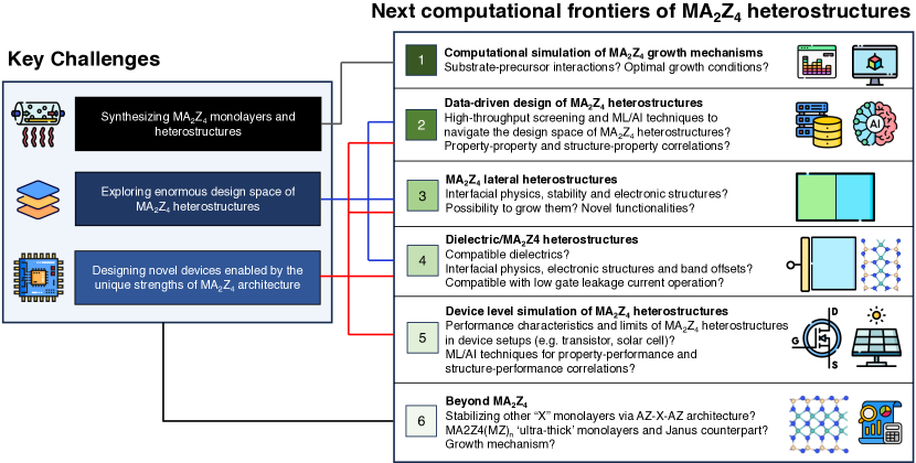
Prospect 3. Data-driven approach of heterostructures design and discovery: High-throughput screening and machine learning models. High-throughput material screening offers an emerging route for the discovery and design of functional 2D materials [192], thanks to the recent advancements of supercomputing facilities and large-scale material databases, such as 2DMatPedia [193] and C2DB [194, 195]. High-throughput material screening typically starts with a large material database containing hundreds or thousands of initial candidates. The candidate pool is then subsequently reduced based on the sequential implementation of filters with increasing computational cost, such as composing elements, band gap, lattice symmetry, mobility, mechanical/thermodynamical/dynamical stability and so on [196, 197]. The screening process eventually produces a smaller pool of material candidates, in which computationally costly can then be performed to understand the performance characteristics and limits for specific target function(s). Based on high-throughput screening methods, a large variety of 2D materials with specific functionalities, such as ferroelectricity [198], ferroelasticity [199], excitonic solar cell [200], topological insulator [201], high-photocatalysts [202] and superconductivity [203], have been catalogued computationally. High-throughput screening has also been employed to the discovery 2D/2D heterostructures, for examples, for solar cell and electrodes applications. However, it should be noted that due to the enormous design space of 2D material heterostructures, the procedures is often limited by: (i) the use of oversimplified methods, such as the Anderson rule which omits the important interfacial interactions between the two contacting surfaces; (ii) a smaller initial candidate pool for screening to reduce the computational cost, which may not fully capture high-performing candidates that lie beyond the smaller initial candidate pool.
High-throughput screening combined with machine learning (ML) methods provide an alternatively route towards data-driven material design and discovery. For example, the band alignment types of 2D/2D heterostructures have been investigated using ML models in recent works [204, 205, 206]. Explicit DFT calculations is first conducted to form the training and testing dataset. An appropriate ML model is first trained using monolayer properties, such as the band edge positions, which are computationally less costly or are readily available in existing material databases. The validity ML model prediction is then verified using the test dataset. Such ML-based method generates useful property-property correlation that streamlines the discovery of new heterostructures and accelerates the prediction of their performance characteristics wihtout the need of costly explicit DFT calculations. Furthermore, ML models can also be used to extract structure-property correlations, which are particularly useful in understanding how structural defects are correlated with the material properties [207].
The emergence of data-driven material discovery and design approaches, either based solely on high-throughput ‘brute force’ method or a combination of high-throughput and ML methods for property-property and structure-property correlations extractions, shall provide a feasible avenue to tame the enormous design space of MA2Z4 heterostructures. We anticipate high-throughput and ML methods to shed light on the following critical unresolved issues that may impact the performance of electronics and optoelectronics devices based on MA2Z4 and their heterostructures:
(1) Interfacial band alignment - The vdW interactions in 2D/2D heterostructures are beneficial in preserving the brand structures of the constituent monolayers, but interfacial charge transfer is still a commonplace in most contact heterostructures. Such transfer gives rise to a built-in electric dipole potential difference , which shifts the relative band alignments between the two constituent monolayers and causes them to deviate from the Anderson rule [208]. Currently, the determination of requires explicit DFT calculations that are computationally costly. Simple analytical model of that may circumvent DFT calculations are challenging to construct due to the intricate and complex interactions at the contact interface. Here data-driven approach may provide an alternative route to predict without explicit DFT calculations. In particular, ML models can be used to extract generalizable property-property correlations of , i.e. , based on dataset generated via high-throughput heterostructure DFT calculations, thus resurrecting the Anderson rule using as a correction term. Similar data-driven approach can also be implemented in MS contact heterostructures for the rapid identification of SBH values.
(2) Interfacial defects - Defects are known to substantially modulate the interfacial properties of 2D materials [209]. The diverse choices of atomic site substitution in MA2Z4, together with the large combinatorial space of contact heterostructures (i.e. stacking orientations and material combinations [210]) shall be benefited from the high-throughput and ML approach.
(3) Heterostructure device performance - A more ambitious application of data-driven method is the extraction of direct correlations between structure, property and device-level performance (such as carrier mobility and solar cell power conversion efficiency), namely the structure-performance and property-performance correlations. ML techniques have been previously demonstrated in the modelling of transistor, such as compact modelling [211, 212] and failure analysis [213, 214], chiefly at the device level. How the data-driven approach can be utilized to link the material-level properties and device-level performance characteristics, which are otherwise challenging and overly complex using physics-based models, remain an open question thus far. Such a data-driven correlations extraction workflow is expected to involve the generation of large dataset using high-throughput DFT simulations and additional device-level simulations (also see Prospect 4 below), before employing ML model to extract practically useful structure-performance and property-performance correlations. We anticipate such data-driven extractions of structure-performance and property-performance correlations to provide a powerful platform for accelerating the design of MA2Z4 heterostructure devices, which can potentially be further generalized to other classes of 2D materials and devices.
Finally, we note that the constructions of ML models require sufficiently large data sets. Due to the limited availability of experimental data, computationally generated data shall play an important role for ML model constructions for MA2Z4 heterostructure design. Such computational data sets can be generated via automated high-throughput calculation workflow that scan through existing large material databases [193, 195]. Apart from performing explicit high-throughput DFT calculations for data generation, specialized small data ML methods, such as imbalance data learning, transfer learning, and active learning, can also be used to tackle the challenges of limited data sets, and such methods have been widely employed in material science research [215].
Prospect 4. Device-level simulation and novel device architectures. Although -based vdWHs have been predicted to exhibit myriads of promising capabilities for device applications, most of the theoretical predictions report only the basic physical quantities (e.g. band alignment, absorption coefficients and Schottky barrier heights), but the performance at the device level (such as transistor, photodetector and solar cell) remains largely unexplored thus far. Such device-level simulations are urgently needed to convincingly establish the technological and industrial relevance of -based heterostructures. Furthermore, novel functional devices, beyond current or conventional device architecture, that are uniquely enabled by the material properties of MA2Z4-based vdWHs has rarely been explored, such as investigation into the nanodiode architecture based on graphene/MoSi2N4/NbS2. We thus expect the computational device simulations and novel device designs to be the next key areas to explore. The simulation results can also be incorporated with high-throughput and ML methods as discussed in Prospect 4 above to yield useful device design rules.
Prospect 5. Dielectric/MA2Z4 heterostructures. Recent investigations of MA2Z4 heterostructures focus mainly on MS and SS contact types. Interfacing MA2Z4 with dielectric materials, such as 3D bulk dielectrics of SiO2 and HfO2 [216] as well as the emerging 2D counterparts [217, 218], such as hBN [219] and Bi2SeO5 [220], has yet to be systematically explored thus far. As dielectric/semiconductor interface is an indispensable component of FET [216], the important contact class of dielectric/MA2Z4 heterostructures is expected to yield important knowledge on the feasibility of MA2Z4 in electronics applications. Importantly, an appropriately engineered dielectric interface, such as the use of high-k dielectrics [221] and dielectric substrate roughness [222, 223], can lead to mobility enhancement in 2D semiconductor. Scrutinizing the interfacial contact physics of dielectric/MA2Z4 heterostructures is thus expected to yield insights on the following open research questions: (i) Does dielectric/MA2Z4 interface exhibit ideal band alignment with sufficiently large conduction and/or valance band offsets that are desirable in suppressing the gate leakage current? (ii) In 2D semiconductors like TMDC, the pristine surfaces have proved to be a double edge sword, useful in preserving carrier mobility down to the monolayer limit, but also severely limiting the dielectric integration via industrial techniques such as atomic layer deposition as precursor nucleation is inhibited. Will MA2Z4 face similar challenges in dielectric integration? (iii) Can high-k dielectric be used to enhance the carrier mobility in an appropriately designed dielectric/MA2Z4 interface? We propose dielectric/MA2Z4 contact heterostructures to be one of the next frontiers of MA2Z4 heterostructure research.
Prospect 6. MA2Z4 lateral heterostructures. Laterally stitched -based heterostructures remains a largely unexplored area. Such heterostructure architecture can be beneficial for lowering contact resistance when compared to vertical heterostructures which are often plagued by the presence of a vdW tunneling barrier [224]. Furthermore, as current state-of-the-art methods of degenerately doping the source and drain contacts of the silicon FET to lower contact resistance poses a huge challenge to map onto atomically thin materials, the growth of lateral MS heterostructures can provide a route to seamlessly attach metallic and semiconducting monolayers together, thus circumventing the need of degenerately doping the source and drain contact.
In fact, the design space of lateral heterostructures is comparable, if not larger, than that of the vertical heterostructures. The construction of lateral heterostructure involves: (1) materials combination; (2) stitching configuration; and (3) defects. Furthermore, because the monolayers are covalently bonded with potentially larger lattice distortion [225], in contrast to the weak vdW coupling of vertical heterostructures, the structural stability can be a more severe issue for lateral heterostructures. This aspect necessitates more a stringent stability verification via phonon spectrum, AIMD and elastic calculations, thus suggesting a higher computational cost. Importantly, unlike vertical heterostructure stacking, lateral stitching of two 2D materials cannot be achieved via mechanical transfer [226, 227]. The growth mechanism of lateral MA2Z4 heterostructures (related to Prospect 2 above) is thus expected to serve as a key practicality indicator that is useful to avoid the ‘pseudo-discovery’ of spurious lateral heterostructure that cannot be realized experimentally. We thus expect computational studies of lateral heterostructures to be another vibrant area of MA2Z4 heterostructures research.
Prospect 7. Generalizing the intercalation architecture for designing novel AZ--AZ monolayer. One of the original motivations of synthesizing MoSi2N4 and WSi2N4 monolayers is to demonstrate that the unstable transition metal nitride monolayers (i.e. MoN2 and WN2) can be stabilized using Si-N outer layers based on an intercalation architecture with SiN-MoN2-SiN morphology [15]. Such approach motivates the discovery of the broader MA2Z4 family [18] with the morphology of AZ-MZ2-AZ. Very recently, such intercalation architecture has been applied to graphene, yielding CSiN monolayer with the same morphology, i.e. SiN-graphene-SiN [228]. This exploration opens up the question of whether such intercalation approach can be generalized to stabilize other monolayers that are relatively unstable or prone to rapid degradation under ambient conditions, such as the sister structures of graphene [229] including silicene [230], germanene [231], stanene [232] and phosphorene [233]. We expect the computational exploration of AZ--AZ monolayers, where is an inherently unstable monolayer or monolayer prone to rapid degradation, and how such synthetic monolayers can be grown via CVD method (related to Prospect 2 above) to represent another exciting frontiers to explore beyond the ‘conventional’ MA2Z4 family.
VI.3 Summary of challenges and new computational frontiers of MA2Z4 heterostructure.
We summarize the challenges and potential new computational/theoretical research frontiers for the MA2Z4 heterostructure outlined in Sections VI.A and VI.B above in Fig. 15. Computational tools, such as DFT, MD and quantum transport device simulations, can potentially address the three key challenges of MA2Z4 heterostructures, namely (i) synthesizing MA2Z4 monolayers beyond MoSi2N4 and WSi2N4 monolayers [15] as well as their heterostructures; (ii) how to efficiently navigate through the enormously large design space of MA2Z4 heterostructures; and (iii) constructing a comprehensive ‘catalogue’ of performance characterization and limits for the expansive family of MA2Z4 heterosturctures, via six research directions which remains largely incomplete thus far (see Fig. 14). For instance, the growth mechanisms (Frontier 1) shall yield insights that can accelerate the experimental realization of MA2Z4 monolayers and heterostructures [i.e. Challenge (i)]. Data-driven approach and the investigations of lateral heterostructure as well as dielectric/MA2Z4 contacts (Frontiers 2 to 4) shall enable the interfacial physics, properties and the design guidelines of MA2Z4 heterostructures to be better understood, thus closing some of the knowledge gap related to Challenge (ii). Frontiers 2 to 4, combined with device-level simulations, shall enable the performance characterizations and limits to be catalogued for conventional devices (such as sub-10-nm transistor and solar cell) as well as novel functional devices (such as spintronic and valleytronic devices), thus addressing Challenge (iii). Finally, the computational material discovery and design outlined in Frontier 6 may yield (1) new subfamily that exhibits a similar intercalation morphology of AZ--AZ; (ii) ultra-thick monolayers of MA2Z4(MZ)n; and (iii) various Janus variations of (i) and (ii), which shall further enrich the field of MA2Z4 heterostructure.
VII Conclusion
In summary, the interfacial properties and contact types of MA2Z4-based heterostructures have been reviewed. MA2Z4-based heterostructures provide a versatile platform to explore a myriad of next-generation devices that are critically needed to resolve some of the ongoing challenges, such as beyond silicon nanoelectronics and clean energy technologies. For -based MS contacts, the tunnelling probability and specific resistivity across the MS vdWHs are more favourable when the monolayer is in contact with 3D metals. On the other hand, -based SS vdWHs can be classified into either Type-I, Type-II, Type-III or Type-H, whereby Type-II category has been extensively studied due to the solar cell and photocatalytic ability of these materials. Type-II -based SS vdWHs with a strong intrinsic electric field not only promote the efficient spatial separation of electrons and holes, but also surmounts the minimum 1.23 eV bandgap requirement for water splitting through either partaking in the Z-scheme photocatalytic process or aided by the additional potential provided by the vacuum level offset at the different monolayers. The photocatalytic abilities of -based heterostructures further suggest their capabilities in high-performance renewable energy applications which are critically needed to achieve sustainable future development. Finally, we discussed the challenges and potential new frontiers of -based heterostructures. We hope that the prospects presented in this work can provide potential new directions on the computational and theoretical simulations of heterostructures that may potentially lead to fruitful results after the initial ‘gold rush’ of research.
Supplementary Material
See the supplementary material for data plotted in Fig. 14.
Acknowledgement
This work is funded by the Singapore Ministry of Education (MOE) Academic Research Fund (AcRF) Tier 2 Grant (MOE-T2EP50221-0019) and SUTD-ZJU IDEA Visiting Professor Grant (SUTD-ZJU (VP) 202001). Figure 15 has been designed using images from Flaticon.com.
Author Declarations
Conflicts of Interest
The authors have no conflicts to disclose.
Author Contributions
Che Chen Tho: Data curation (lead); Formal analysis (lead); Investigation (equal); Writing – original draft (equal); Visualization (lead); Writing – review & editing (supporting); San-Dong Guo: Writing – review & editing (supporting); Shi-Jun Liang: Writing – review & editing (supporting); Wee Liat Ong: Writing – review & editing (supporting); Chit Siong Lau: Writing – review & editing (supporting); Liemao Cao: Writing – review & editing (supporting); Guangzhao Wang: Conceptualization (supporting); Data curation (supporting); Writing – original draft (supporting); Writing – review & editing (supporting); Yee Sin Ang: Conceptualization (lead); Investigation (equal); Formal analysis (supporting); Supervision (lead); Funding acquisition (lead); Visualization (supporting); Writing – original draft (equal); Writing – review & editing (lead).
Data Availability Statement
Data sharing is not applicable to this article as no new data were created in this study.
References
- Quhe et al. [2021] R. Quhe, L. Xu, S. Liu, C. Yang, Y. Wang, H. Li, J. Yang, Q. Li, B. Shi, Y. Li, et al., Sub-10 nm two-dimensional transistors: Theory and experiment, Phys. Rep. 938, 1 (2021).
- Wang et al. [2018a] L. Wang, L. Huang, W. C. Tan, X. Feng, L. Chen, X. Huang, and K.-W. Ang, 2d photovoltaic devices: progress and prospects, Small Methods 2, 1700294 (2018a).
- Wang et al. [2022a] G. Wang, J. Chang, W. Tang, W. Xie, and Y. S. Ang, 2d materials and heterostructures for photocatalytic water-splitting: A theoretical perspective, J. Phys. D 55, 293002 (2022a).
- Zhang et al. [2016a] X. Zhang, L. Hou, A. Ciesielski, and P. Samorì, 2d materials beyond graphene for high-performance energy storage applications, Adv. Energy Mater. 6, 1600671 (2016a).
- Huh et al. [2020] W. Huh, D. Lee, and C.-H. Lee, Memristors based on 2d materials as an artificial synapse for neuromorphic electronics, Adv. Mater. 32, 2002092 (2020).
- Goh et al. [2023] K. E. J. Goh, C. P. Y. Wong, and T. Wang, Valleytronics in 2D materials (World Scientific, 2023).
- Vitale et al. [2018] S. A. Vitale, D. Nezich, J. O. Varghese, P. Kim, N. Gedik, P. Jarillo-Herrero, D. Xiao, and M. Rothschild, Valleytronics: opportunities, challenges, and paths forward, Small 14, 1801483 (2018).
- Schaibley et al. [2016] J. R. Schaibley, H. Yu, G. Clark, P. Rivera, J. S. Ross, K. L. Seyler, W. Yao, and X. Xu, Valleytronics in 2d materials, Nat. Rev. Mater. 1, 1 (2016).
- Goh et al. [2020] K. E. J. Goh, F. Bussolotti, C. S. Lau, D. Kotekar-Patil, Z. E. Ooi, and J. Y. Chee, Toward valley-coupled spin qubits, Adv. Quantum Technol. 3, 1900123 (2020).
- Ang et al. [2017] Y. S. Ang, S. A. Yang, C. Zhang, Z. Ma, and L. K. Ang, Valleytronics in merging dirac cones: All-electric-controlled valley filter, valve, and universal reversible logic gate, Phys. Rev. B 96, 245410 (2017).
- Liu and Hersam [2019] X. Liu and M. C. Hersam, 2d materials for quantum information science, Nat. Rev. Mater. 4, 669 (2019).
- Choi et al. [2017] W. Choi, N. Choudhary, G. H. Han, J. Park, D. Akinwande, and Y. H. Lee, Recent development of two-dimensional transition metal dichalcogenides and their applications, Mater. Today 20, 116 (2017).
- Sang et al. [2019] D. K. Sang, H. Wang, Z. Guo, N. Xie, and H. Zhang, Recent developments in stability and passivation techniques of phosphorene toward next-generation device applications, Adv. Funct. Mater. 29, 1903419 (2019).
- Zhang et al. [2016b] S. Zhang, M. Xie, F. Li, Z. Yan, Y. Li, E. Kan, W. Liu, Z. Chen, and H. Zeng, Semiconducting group 15 monolayers: a broad range of band gaps and high carrier mobilities, Angew. Chem. 128, 1698 (2016b).
- Hong et al. [2020] Y.-L. Hong, Z. Liu, L. Wang, T. Zhou, W. Ma, C. Xu, S. Feng, L. Chen, M.-L. Chen, D.-M. Sun, et al., Chemical vapor deposition of layered two-dimensional materials, Science 369, 670 (2020).
- Bafekry et al. [2021a] A. Bafekry, M. Faraji, D. M. Hoat, M. Shahrokhi, M. Fadlallah, F. Shojaei, S. Feghhi, M. Ghergherehchi, and D. Gogova, Mosi2n4 single-layer: a novel two-dimensional material with outstanding mechanical, thermal, electronic and optical properties, J. Phys. D 54, 155303 (2021a).
- Kong et al. [2022] M. Kong, S. Murakami, and T. Zhang, A comprehensive study of complex non-adiabatic exciton dynamics in mosi2n4, Mater. Today Phys. 27, 100814 (2022).
- Wang et al. [2021a] L. Wang, Y. Shi, M. Liu, A. Zhang, Y.-L. Hong, R. Li, Q. Gao, M. Chen, W. Ren, H.-M. Cheng, et al., Intercalated architecture of family layered van der waals materials with emerging topological, magnetic and superconducting properties, Nat. Commun. 12, 1 (2021a).
- Zhao et al. [2021a] H. Zhao, G. Yang, Y. Liu, X. Yang, Y. Gu, C. Wei, Z. Xie, Q. Zhang, B. Bian, X. Zhang, et al., Quantum transport of sub-10 nm monolayer transistors, ACS Appl. Electron. Mater. 3, 5086 (2021a).
- Sun et al. [2021] X. Sun, Z. Song, N. Huo, S. Liu, C. Yang, J. Yang, W. Wang, and J. Lu, Performance limit of monolayer transistors, J. Mater. Chem. C 9, 14683 (2021).
- Huang et al. [2021] J. Huang, P. Li, X. Ren, and Z.-X. Guo, Promising properties of a sub-5-nm monolayer transistor, Phys. Rev. Appl. 16, 044022 (2021).
- Ye et al. [2022] B. Ye, X. Jiang, Y. Gu, G. Yang, Y. Liu, H. Zhao, X. Yang, C. Wei, X. Zhang, and N. Lu, Quantum transport of short-gate mosfets based on monolayer , Phys. Chem. Chem. Phys. 24, 6616 (2022).
- Nandan et al. [2021] K. Nandan, B. Ghosh, A. Agarwal, S. Bhowmick, and Y. S. Chauhan, Two-dimensional : An excellent 2-d semiconductor for field-effect transistors, IEEE Trans. Electron Devices 69, 406 (2021).
- Nandan et al. [2022] K. Nandan, S. Bhowmick, Y. S. Chauhan, and A. Agarwal, Designing power efficient transistors using narrow bandwidth materials from the monolayer series, arXiv:2211.09540 (2022).
- Pham [2021] D. Pham, Electronic properties of a two-dimensional van der waals heterobilayer: Effect of the insertion of a graphene layer and interlayer coupling, RSC Adv. 11, 28659 (2021).
- Shu et al. [2022] L. Shu, L. Qian, X. Ye, and Y. Xie, Multifunctional two-dimensional photodetector driven by the photogalvanic effect, Phys. Rev. Appl. 17, 054010 (2022).
- Tho et al. [2023] C. C. Tho, C. Yu, Q. Tang, Q. Wang, T. Su, Z. Feng, Q. Wu, C. Nguyen, W.-L. Ong, S.-J. Liang, et al., Cataloguing and van der waals heterostructures: An exceptional material platform for excitonic solar cell applications, Adv. Mater. Interfaces 10, 2201856 (2023).
- Guo et al. [2022a] Y. Guo, J. Min, X. Cai, L. Zhang, C. Liu, and Y. Jia, Two-dimensional type-ii vdw heterostructures for high-performance solar cells, J. Phys. Chem. C 126, 4677 (2022a).
- Liu et al. [2022] C. Liu, Z. Wang, W. Xiong, H. Zhong, and S. Yuan, Effect of vertical strain and in-plane biaxial strain on type-ii van der waals heterostructure, J. Appl. Phys. 131, 163102 (2022).
- Nguyen et al. [2022a] C. Q. Nguyen, Y. S. Ang, S.-T. Nguyen, N. V. Hoang, N. M. Hung, and C. V. Nguyen, Tunable type-ii band alignment and electronic structure of heterostructure: Interlayer coupling and electric field, Phys. Rev. B 105, 045303 (2022a).
- Ng et al. [2022a] J. Q. Ng, Q. Wu, L. K. Ang, and Y. S. Ang, Tunable electronic properties and band alignments of and van der waals heterostructures, Appl. Phys. Lett. 120, 103101 (2022a).
- Bafekry et al. [2021b] A. Bafekry, M. Faraji, A. A. Ziabari, M. Fadlallah, C. V. Nguyen, M. Ghergherehchi, and S. Feghhi, A van der waals heterostructure of : a first-principles study, New J. Chem. 45, 8291 (2021b).
- Xuefeng et al. [2022] C. Xuefeng, H. Wenna, J. Minglei, R. Fengzhu, P. Chengxiao, G. Qinfen, W. Bing, and Y. Huabing, A direct z-scheme vdw heterostructure for photocatalytic overall water splitting, J. Phys. D 55, 215502 (2022).
- Zeng et al. [2021] J. Zeng, L. Xu, Y. Yang, X. Luo, H.-J. Li, S. Xiong, and L.-L. Wang, Boosting the photocatalytic hydrogen evolution performance of monolayer coupled with : density-functional theory calculations, Phys. Chem. Chem. Phys. 23, 8318 (2021).
- He et al. [2022] Y. He, Y.-h. Zhu, M. Zhang, J. Du, W.-h. Guo, S.-m. Liu, C. Tian, H.-x. Zhong, X. Wang, and J.-j. Shi, High hydrogen production in the inse/mosi2n4 van der waals heterostructure for overall water splitting, Phys. Chem. Chem. Phys. 24, 2110 (2022).
- Mortazavi et al. [2021] B. Mortazavi, B. Javvaji, F. Shojaei, T. Rabczuk, A. Shapeev, and X. Zhuang, Exceptional piezoelectricity, high thermal conductivity and stiffness and promising photocatalysis in two-dimensional family confirmed by first-principles, Nano Energy 82, 105716 (2021).
- Cai et al. [2021a] X. Cai, Z. Zhang, Y. Zhu, L. Lin, W. Yu, Q. Wang, X. Yang, X. Jia, and Y. Jia, A two-dimensional van der waals heterostructure with high carrier mobility and diversified regulation of its electronic properties, J. Mater. Chem. C 9, 10073 (2021a).
- Cai et al. [2021b] X. Cai, Z. Zhang, A. Song, G. Chen, W. Yu, X. Jia, X. Yang, Y. Liu, and Y. Jia, Indirect to direct bandgap transition and enhanced optoelectronic properties in monolayer through forming bilayer, Available at SSRN 3968855 (2021b).
- Li et al. [2022a] X.-M. Li, Z.-Z. Lin, L.-R. Cheng, and X. Chen, Layered as electrode material of zn–air battery, Phys. Status Solidi - Rapid Res. Lett. 16, 2200007 (2022a).
- Xiao et al. [2022] C. Xiao, Z. Ma, R. Sa, Z. Cui, S. Gao, W. Du, X. Sun, and Q.-h. Li, Adsorption behavior of environmental gas molecules on pristine and defective : Possible application as highly sensitive and reusable gas sensors, ACS Omega 7, 8706 (2022).
- Bafekry et al. [2021c] A. Bafekry, M. Faraji, M. Fadlallah, A. A. Ziabari, A. B. Khatibani, S. Feghhi, M. Ghergherehchi, and D. Gogova, Adsorption of habitat and industry-relevant molecules on the monolayer, Appl. Surf. Sci. 564, 150326 (2021c).
- Zhong et al. [2021] T. Zhong, Y. Ren, Z. Zhang, J. Gao, and M. Wu, Sliding ferroelectricity in two-dimensional (a= si or ge) bilayers: high polarizations and moiré potentials, J. Mater. Chem. A 9, 19659 (2021).
- Geim and Grigorieva [2013] A. K. Geim and I. V. Grigorieva, Van der waals heterostructures, Nature 499, 419 (2013).
- Xin et al. [2022] K. Xin, X. Wang, K. Grove-Rasmussen, and Z. Wei, Twist-angle two-dimensional superlattices and their application in (opto) electronics, J. Semicond. 43, 011001 (2022).
- Pham et al. [2022] P. V. Pham, S. C. Bodepudi, K. Shehzad, Y. Liu, Y. Xu, B. Yu, and X. Duan, 2d heterostructures for ubiquitous electronics and optoelectronics: principles, opportunities, and challenges, Chem. Rev. 122, 6514 (2022).
- Yin et al. [2023] Y. Yin, Q. Gong, M. Yi, and W. Guo, Emerging versatile two-dimensional mosi2n4 family, Adv. Funct. Mater. 33, 2214050 (2023).
- Castellanos-Gomez et al. [2014] A. Castellanos-Gomez, M. Buscema, R. Molenaar, V. Singh, L. Janssen, H. S. J. van der Zant, and G. A. Steele, Deterministic transfer of two-dimensional materials by all-dry viscoelastic stamping, 2d Mater. 1, 011002 (2014).
- Gurarslan et al. [2014] A. Gurarslan, Y. Yu, L. Su, Y. Yu, F. Suarez, S. Yao, Y. Zhu, M. Ozturk, Y. Zhang, and L. Cao, Surface-energy-assisted perfect transfer of centimeter-scale monolayer and few-layer films onto arbitrary substrates, ACS Nano 8, 11522 (2014).
- Cui et al. [2018] X. Cui, Z. Kong, E. Gao, D. Huang, Y. Hao, H. Shen, C.-a. Di, Z. Xu, J. Zheng, and D. Zhu, Rolling up transition metal dichalcogenide nanoscrolls via one drop of ethanol, Nat. Commun. 9, 1301 (2018).
- Desai et al. [2016] S. B. Desai, S. R. Madhvapathy, M. Amani, D. Kiriya, M. Hettick, M. Tosun, Y. Zhou, M. Dubey, J. W. Ager III, D. Chrzan, and A. Javey, Gold-mediated exfoliation of ultralarge optoelectronically-perfect monolayers, Adv. Mater. 28, 4053 (2016).
- Zaretski and Lipomi [2015] A. V. Zaretski and D. J. Lipomi, Processes for non-destructive transfer of graphene: widening the bottleneck for industrial scale production, Nanoscale 7, 9963 (2015).
- Zaretski et al. [2015] A. V. Zaretski, H. Moetazedi, C. Kong, E. J. Sawyer, S. Savagatrup, E. Valle, T. F. O’Connor, A. D. Printz, and D. J. Lipomi, Metal-assisted exfoliation (mae): green, roll-to-roll compatible method for transferring graphene to flexible substrates, Nanotechnology 26, 045301 (2015).
- Bae et al. [2017] S.-H. Bae, X. Zhou, S. Kim, Y. S. Lee, S. S. Cruz, Y. Kim, J. B. Hannon, Y. Yang, D. K. Sadana, F. M. Ross, H. Park, and J. Kim, Unveiling the carrier transport mechanism in epitaxial graphene for forming wafer-scale, single-domain graphene, PNAS 114, 4082 (2017).
- Wang et al. [2021b] J. Wang, X. Zhao, G. Hu, J. Ren, and X. Yuan, Manipulable electronic and optical properties of two-dimensional van der waals heterostructures, Nanomaterials 11, 3338 (2021b).
- Hussain et al. [2022a] G. Hussain, M. Asghar, M. W. Iqbal, H. Ullah, and C. Autieri, Exploring the structural stability, electronic and thermal attributes of synthetic 2d materials and their heterostructures, Appl. Surf. Sci. 590, 153131 (2022a).
- Ren et al. [2022] Y.-T. Ren, L. Hu, Y.-T. Chen, Y.-J. Hu, J.-L. Wang, P.-L. Gong, H. Zhang, L. Huang, and X.-Q. Shi, Two-dimensional monolayers and van der waals heterostructures: Promising spintronic properties and band alignments, Phys. Rev. Mater. 6, 064006 (2022).
- Zhao et al. [2021b] J. Zhao, X. Jin, H. Zeng, C. Yao, and G. Yan, Spin-valley coupling and valley splitting in the van der waals heterostructure, Appl. Phys. Lett. 119, 213101 (2021b).
- Besse et al. [2021a] R. Besse, J. F. Silveira, Z. Jiang, D. West, S. Zhang, and J. L. Da Silva, Beyond the anderson rule: importance of interfacial dipole and hybridization in van der waals heterostructures, 2d Mater. 8, 041002 (2021a).
- Tersoff [1984] J. Tersoff, Theory of semiconductor heterojunctions: The role of quantum dipoles, Phys. Rev. B 30, 4874 (1984).
- Koda et al. [2017] D. S. Koda, F. Bechstedt, M. Marques, and L. K. Teles, Tuning electronic properties and band alignments of phosphorene combined with and , J. Phys. Chem. C 121, 3862 (2017).
- Liang et al. [2023] Q. Liang, X. Luo, G. Qian, Y. Wang, Y. Wang, Y. Liang, and Q. Xie, Van der waals stacking-induced efficient ohmic contacts and the weak fermi level pinning effect in and contact with two-dimensional metals, Physica E Low Dimens. Syst. Nanostruct. 149, 115686 (2023).
- Nguyen et al. [2022b] C. V. Nguyen, C. Q. Nguyen, S.-T. Nguyen, Y. S. Ang, and N. V. Hieu, Two-dimensional metal/semiconductor contact in a janus van der waals heterostructure, J. Phys. Chem. Lett. 13, 2576 (2022b).
- Li et al. [2023a] Z. Li, J. Han, S. Cao, and Z. Zhang, Graphene/mosi2x4: A class of van der waals heterojunctions with unique mechanical and optical properties and controllable electrical contacts, Appl. Surf. Sci. 614, 156095 (2023a).
- Ma et al. [2023] X. Ma, H. Bo, X. Gong, G. Yuan, Z. Peng, J. Lu, and Q. Xie, Tunable schottky barrier of wsi2n4/graphene heterostructure via interface distance and external electric field, Appl. Surf. Sci. 615, 156385 (2023).
- He et al. [2023] X. He, W. Li, Z. Gao, Z. Zhang, and Y. He, Achieving real ohmic contact by the dual protection of outer layer atoms and surface functionalization in 2d metal mxenes/mosi2n4 heterostructures, J. Mater. Chem. C 11, 4728 (2023).
- Zhang et al. [2023a] X. Zhang, J.-Y. Zheng, Y.-C. Xiang, D. Wu, J. Fan, Y.-Y. Sun, L.-J. Chen, L.-Y. Gan, and X. Zhou, Ohmic contacts in mxene/mosi2n4 heterojunctions, Appl. Phys. Lett. 123 (2023a).
- Cao et al. [2021] L. Cao, G. Zhou, Q. Wang, L. K. Ang, and Y. S. Ang, Two-dimensional van der waals electrical contact to monolayer , Appl. Phys. Lett. 118, 013106 (2021).
- Binh et al. [2021] N. T. T. Binh, C. Q. Nguyen, T. V. Vu, and C. V. Nguyen, Interfacial electronic properties and tunable contact types in graphene/janus- heterostructures, J. Phys. Chem. Lett. 12, 3934 (2021).
- Guo et al. [2022b] Y. Guo, Y. Dong, X. Cai, L. Liu, and Y. Jia, Controllable schottky barriers and contact types of bn intercalation layers in vdw heterostructures via applying an external electrical field, Phys. Chem. Chem. Phys. 24, 18331 (2022b).
- Yuan et al. [2022] G. Yuan, Z. Cheng, Y. Cheng, W. Duan, H. Lv, Z. Liu, C. Han, and X. Ma, Highly sensitive band alignment of the heterojunction via an external electric field, ACS Appl. Electron. Mater. 4, 2897 (2022).
- Tung [2014] R. T. Tung, The physics and chemistry of the schottky barrier height, Appl. Phys. Rev. 1, 011304 (2014).
- Kang et al. [2014] J. Kang, W. Liu, D. Sarkar, D. Jena, and K. Banerjee, Computational study of metal contacts to monolayer transition-metal dichalcogenide semiconductors, Phys. Rev. X 4, 031005 (2014).
- Liu et al. [2016] Y. Liu, P. Stradins, and S.-H. Wei, Van der waals metal-semiconductor junction: Weak fermi level pinning enables effective tuning of schottky barrier, Sci. Adv. 2, e1600069 (2016).
- Ang et al. [2021] Y. S. Ang, L. Cao, and L. K. Ang, Physics of electron emission and injection in two-dimensional materials: Theory and simulation, InfoMat 3, 502 (2021).
- Sze et al. [2021] S. M. Sze, Y. Li, and K. K. Ng, Physics of semiconductor devices (John wiley & sons, 2021).
- Li et al. [2022b] J. Li, W. Zhou, L. Xu, J. Yang, H. Qu, T. Guo, B. Xu, S. Zhang, and H. Zeng, Revealing the weak fermi level pinning effect of 2d semiconductor/2d metal contact: A case of monolayer in2ge2te6 and its janus structure in2ge2te3se3, Materials Today Physics 26, 100749 (2022b).
- Wang et al. [2021c] Q. Wang, L. Cao, S.-J. Liang, W. Wu, G. Wang, C. H. Lee, W. L. Ong, H. Y. Yang, L. K. Ang, S. A. Yang, and Y. S. Ang, Efficient ohmic contacts and built-in atomic sublayer protection in and monolayers, NPJ 2D Mater. Appl. 5, 71 (2021c).
- Wu et al. [2022] Y. Wu, Z. Tang, W. Xia, W. Gao, F. Jia, Y. Zhang, W. Zhu, W. Zhang, and P. Zhang, Prediction of protected band edge states and dielectric tunable quasiparticle and excitonic properties of monolayer mosi2n4, npj Computational Materials 8, 129 (2022).
- Simmons [1963] J. G. Simmons, Generalized formula for the electric tunnel effect between similar electrodes separated by a thin insulating film, J. Appl. Phys. 34, 1793 (1963).
- Shen et al. [2021] P.-C. Shen, C. Su, Y. Lin, A.-S. Chou, C.-C. Cheng, J.-H. Park, M.-H. Chiu, A.-Y. Lu, H.-L. Tang, M. M. Tavakoli, et al., Ultralow contact resistance between semimetal and monolayer semiconductors, Nature 593, 211 (2021).
- Li et al. [2023b] Q. Li, C. Yang, L. Xu, S. Liu, S. Fang, L. Xu, J. Yang, J. Ma, Y. Li, B. Wu, et al., Symmetric and excellent scaling behavior in ultrathin n-and p-type gate-all-around inas nanowire transistors, Adv. Funct. Mater. , 2214653 (2023b).
- Zhang et al. [2023b] Q.-K. Zhang, W.-H. Zhao, Z.-P. Zhou, L.-M. Cao, W.-J. Yin, X.-L. Wei, Z.-K. Tang, and H. Zhang, 2d janus mosse/mogesin4 vdw heterostructures for photovoltaic and photocatalysis applications, J. Alloys Compd. 938, 168708 (2023b).
- Pei et al. [2023] M. Pei, X. Zhao, C. Xia, T. Wang, X. Dai, and S. Wei, Tuning the band alignment and electronic properties of xse2/wsi2n4 (x = mo, w) van der waals heterostructures with high carrier mobility, Physica E Low Dimens. Syst. Nanostruct. 149, 115656 (2023).
- Zhao et al. [2022a] P. Zhao, Z.-Y. Jiang, J.-M. Zheng, Y.-M. Lin, and A. Du, Theoretical study of a novel heterostructure with ultrafast carrier transport, J. Phys. Chem. C 126, 11380 (2022a).
- Yu et al. [2021] Y. Yu, J. Zhou, Z. Guo, and Z. Sun, Novel two-dimensional janus and as highly efficient photocatalysts for spontaneous overall water splitting, ACS Appl. Mater. Interfaces 13, 28090 (2021).
- Ren et al. [2023] K. Ren, H. Shu, K. Wang, and H. Qin, Two-dimensional mx2y4 systems: Ultrahigh carrier transport and excellent hydrogen evolution reaction performances, Phys. Chem. Chem. Phys. 25, 4519 (2023).
- Lv et al. [2022] X. Lv, H. Huang, B. Mao, G. Liu, G. Zhao, and J. Yang, Dipole-regulated bandgap and high electron mobility for bilayer janus , Appl. Phys. Lett. 120, 213101 (2022).
- Shu et al. [2023] Y. Shu, Y. Liu, Z. Cui, R. Xiong, Y. Zhang, C. Xu, J. Zheng, C. Wen, B. Wu, and B. Sa, Efficient ohmic contact in monolayer crx2n4 (x= c, si) based field-effect transistors, Adv. Electron. Mater. 9, 2201056 (2023).
- Wang et al. [2022b] S. Wang, X. Liu, and P. Zhou, The road for 2d semiconductors in the silicon age, Adv. Mater. 34, 2106886 (2022b).
- Xu et al. [2023a] X. Xu, L. Yang, Q. Gao, X. Jiang, D. Li, B. Cui, and D. Liu, Type-ii van der waals heterostructure with excellent optoelectronic performance and tunable electronic properties, J. Phys. Chem. C 127, 7878 (2023a).
- Fang et al. [2022] L. Fang, Y. Ni, J. Hu, Z. Tong, X. Ma, H. Lv, and S. Hou, First-principles insights of electronic properties of blue van der waals heterostructure via vertical electric field and biaxial strain, Physica E Low Dimens. Syst. Nanostruct. 143, 115321 (2022).
- Nguyen et al. [2020] H. T. Nguyen, M. M. Obeid, A. Bafekry, M. Idrees, T. V. Vu, H. V. Phuc, N. N. Hieu, L. T. Hoa, B. Amin, and C. V. Nguyen, Interfacial characteristics, schottky contact, and optical performance of a van der waals heterostructure: Strain engineering and electric field tunability, Phys. Rev. B 102, 075414 (2020).
- Huang et al. [2019] S. Huang, G. Zhang, F. Fan, C. Song, F. Wang, Q. Xing, C. Wang, H. Wu, and H. Yan, Strain-tunable van der waals interactions in few-layer black phosphorus, Nat. Commun. 10, 2447 (2019).
- Dienwiebel et al. [2004] M. Dienwiebel, G. S. Verhoeven, N. Pradeep, J. W. M. Frenken, J. A. Heimberg, and H. W. Zandbergen, Superlubricity of graphite, Phys. Rev. Lett. 92, 126101 (2004).
- Tongay et al. [2014] S. Tongay, W. Fan, J. Kang, J. Park, U. Koldemir, J. Suh, D. S. Narang, K. Liu, J. Ji, J. Li, R. Sinclair, and J. Wu, Tuning interlayer coupling in large-area heterostructures with cvd-grown and monolayers, Nano Lett. 14, 3185 (2014).
- Fang et al. [2014] H. Fang, C. Battaglia, C. Carraro, S. Nemsak, B. Ozdol, J. S. Kang, H. A. Bechtel, S. B. Desai, F. Kronast, A. A. Unal, G. Conti, C. Conlon, G. K. Palsson, M. C. Martin, A. M. Minor, C. S. Fadley, E. Yablonovitch, R. Maboudian, and A. Javey, Strong interlayer coupling in van der waals heterostructures built from single-layer chalcogenides, PNAS 111, 6198 (2014).
- Bardeen and Shockley [1950] J. Bardeen and W. Shockley, Deformation potentials and mobilities in non-polar crystals, Phys. Rev. 80, 72 (1950).
- Lang et al. [2016] H. Lang, S. Zhang, and Z. Liu, Mobility anisotropy of two-dimensional semiconductors, Phys. Rev. B 94, 235306 (2016).
- Mir et al. [2020a] S. H. Mir, V. K. Yadav, and J. K. Singh, Recent advances in the carrier mobility of two-dimensional materials: a theoretical perspective, ACS Omega 5, 14203 (2020a).
- Gregg [2003] B. A. Gregg, Excitonic solar cells (2003).
- Silveira et al. [2022] J. F. Silveira, R. Besse, A. C. Dias, N. A. Caturello, and J. L. Da Silva, Tailoring excitonic and optoelectronic properties of transition metal dichalcogenide bilayers, J. Phys. Chem. C 126, 9173 (2022).
- Tian et al. [2021] Y. Tian, A. Sun, Z. Ge, Y. Zhang, S. Huang, S. Lv, and H. Li, Strain tunable electronic states of monolayer, Chem. Phys. Lett. 765, 138286 (2021).
- Fu et al. [2018a] C.-F. Fu, J. Sun, Q. Luo, X. Li, W. Hu, and J. Yang, Intrinsic electric fields in two-dimensional materials boost the solar-to-hydrogen efficiency for photocatalytic water splitting, Nano Lett. 18, 6312 (2018a).
- Jalil et al. [2023] A. Jalil, T. Zhao, A. Kanwal, and I. Ahmed, Prediction of direct z-scheme h and H́-phase of (x= s, se) van der waals heterostructures: A promising candidate for photocatalysis, Chem. Eng. J. , 144239 (2023).
- Liu et al. [2023a] Y. Liu, Z. Jiang, J. Jia, J. Robertson, and Y. Guo, 2d wse2/mosi2n4 type-ii heterojunction with improved carrier separation and recombination for photocatalytic water splitting, Appl. Surf. Sci. 611, 155674 (2023a).
- Li et al. [2022c] R.-X. Li, X.-L. Tian, S.-C. Zhu, Q.-H. Mao, J. Ding, and H.-D. Li, van der waals heterostructure with high solar-to-hydrogen efficiency, Physica E Low Dimens. Syst. Nanostruct. 144, 115443 (2022c).
- Fu et al. [2018b] C.-F. Fu, X. Wu, and J. Yang, Material design for photocatalytic water splitting from a theoretical perspective, Adv. Mater. 30, 1802106 (2018b).
- Chen et al. [2017] S. Chen, T. Takata, and K. Domen, Particulate photocatalysts for overall water splitting, Nat. Rev. Mater. 2, 1 (2017).
- Kudo and Miseki [2009] A. Kudo and Y. Miseki, Heterogeneous photocatalyst materials for water splitting, Chem. Soc. Rev. 38, 253 (2009).
- Liu et al. [2018] G. Liu, C. Zhen, Y. Kang, L. Wang, and H.-M. Cheng, Unique physicochemical properties of two-dimensional light absorbers facilitating photocatalysis, Chem. Soc. Rev. 47, 6410 (2018).
- Su et al. [2018] T. Su, Q. Shao, Z. Qin, Z. Guo, and Z. Wu, Role of interfaces in two-dimensional photocatalyst for water splitting, ACS Catal. 8, 2253 (2018).
- Chen and Tang [2021] J. Chen and Q. Tang, The versatile electronic, magnetic and photo-electro catalytic activity of a new 2d family, Chem. Eur. J 27, 9925 (2021).
- Jian et al. [2021] C.-c. Jian, X. Ma, J. Zhang, and X. Yong, Strained monolayers with excellent solar energy absorption and carrier transport properties, J. Phys. Chem. C 125, 15185 (2021).
- Rehman et al. [2022] S. U. Rehman, Z. Tariq, F. K. Butt, X. Zhang, B. U. Haq, and C. Li, Novel two-dimensional (m= cr, mo, w) monolayers for overall water splitting with high visible-light absorption, Sol Energy 241, 416 (2022).
- Lin et al. [2022] C. Lin, X. Feng, D. Legut, X. Liu, Z. W. Seh, R. Zhang, and Q. Zhang, Discovery of efficient visible-light driven oxygen evolution photocatalysts: Automated high-throughput computational screening of , Adv. Funct. Mater. 32, 2207415 (2022).
- Zhang et al. [2022a] W. Zhang, W. Yang, Y. Liu, Z. Liu, and F. Zhang, Computational exploration and screening of novel janus (m= sc-zn, y-ag, hf-au; a= si, ge; z= n, p) monolayers and potential application as a photocatalyst, Front. Phys. 17, 63509 (2022a).
- Li et al. [2014] X. Li, Z. Li, and J. Yang, Proposed photosynthesis method for producing hydrogen from dissociated water molecules using incident near-infrared light, Phys. Rev. Lett. 112, 018301 (2014).
- Peng et al. [2019] R. Peng, Y. Ma, B. Huang, and Y. Dai, Two-dimensional janus ptsse for photocatalytic water splitting under the visible or infrared light, J. Mater. Chem. A 7, 603 (2019).
- Ma et al. [2018] X. Ma, X. Wu, H. Wang, and Y. Wang, A janus mosse monolayer: a potential wide solar-spectrum water-splitting photocatalyst with a low carrier recombination rate, J. Mater. Chem. A 6, 2295 (2018).
- Ju et al. [2020] L. Ju, M. Bie, X. Tang, J. Shang, and L. Kou, Janus wsse monolayer: an excellent photocatalyst for overall water splitting, ACS Appl. Mater. Interfaces 12, 29335 (2020).
- Luo et al. [2021] Y. Luo, M. Sun, J. Yu, and U. Schwingenschlogl, , , and : candidate two-dimensional janus materials for photocatalytic water splitting, Chem. Mater. 33, 4128 (2021).
- Moniz et al. [2015] S. J. Moniz, S. A. Shevlin, D. J. Martin, Z.-X. Guo, and J. Tang, Visible-light driven heterojunction photocatalysts for water splitting–a critical review, Energy & Environmental Science 8, 731 (2015).
- Wang et al. [2014a] H. Wang, L. Zhang, Z. Chen, J. Hu, S. Li, Z. Wang, J. Liu, and X. Wang, Semiconductor heterojunction photocatalysts: design, construction, and photocatalytic performances, Chem. Soc. Rev. 43, 5234 (2014a).
- Zhou et al. [2021] Z. Zhou, S. Yuan, and J. Wang, Theoretical progress on direct z-scheme photocatalysis of two-dimensional heterostructures, Front. Phys. 16, 1 (2021).
- Huang et al. [2022] X. Huang, L. Xu, B. Xiao, K. Dong, K. Yang, L. Li, and L.-L. Wang, High-efficiency photocatalyst based on a heterojunction, J. Mater. Sci. 57, 16404 (2022).
- Cao et al. [2018] Y. Cao, V. Fatemi, S. Fang, K. Watanabe, T. Taniguchi, E. Kaxiras, and P. Jarillo-Herrero, Unconventional superconductivity in magic-angle graphene superlattices, Nature 556, 43 (2018).
- Linghu et al. [2018a] J. Linghu, T. Yang, Y. Luo, M. Yang, J. Zhou, L. Shen, and Y. P. Feng, High-throughput computational screening of vertical 2d van der waals heterostructures for high-efficiency excitonic solar cells, ACS Appl. Mater. Interfaces 10, 32142 (2018a).
- Kaur et al. [2018] S. Kaur, A. Kumar, S. Srivastava, K. Tankeshwar, and R. Pandey, Monolayer, bilayer, and heterostructures of green phosphorene for water splitting and photovoltaics, J. Phys. Chem. C 122, 26032 (2018).
- Huang et al. [2020] X. Huang, L. Zhou, L. Yan, Y. Wang, W. Zhang, X. Xie, Q. Xu, and H.-Z. Song, (x = cl, br, i) monolayer and type ii heterostructures with promising photovoltaic characteristics, Chinese Phys. Lett. 37, 127101 (2020).
- Mohanta et al. [2019] M. K. Mohanta, A. Rawat, N. Jena, Dimple, R. Ahammed, and A. De Sarkar, Interfacing boron monophosphide with molybdenum disulfide for an ultrahigh performance in thermoelectrics, two-dimensional excitonic solar cells, and nanopiezotronics, ACS Appl. Mater. Interfaces 12, 3114 (2019).
- Mohanta et al. [2020] M. K. Mohanta, A. Kishore, and A. De Sarkar, Two-dimensional ultrathin van der waals heterostructures of indium selenide and boron monophosphide for superfast nanoelectronics, excitonic solar cells, and digital data storage devices, Nanotechnology 31, 495208 (2020).
- Mao et al. [2019] Y. Mao, C. Xu, J. Yuan, and H. Zhao, A two-dimensional gese/snse heterostructure for high performance thin-film solar cells, J. Mater. Chem. A 7, 11265 (2019).
- Xie et al. [2016] M. Xie, S. Zhang, B. Cai, Y. Huang, Y. Zou, B. Guo, Y. Gu, and H. Zeng, A promising two-dimensional solar cell donor: Black arsenic–phosphorus monolayer with 1.54 ev direct bandgap and mobility exceeding 14,000 cm2v-1s-1, Nano Energy 28, 433 (2016).
- Wang et al. [2018b] X. Wang, R. Quhe, W. Cui, Y. Zhi, Y. Huang, Y. An, X. Dai, Y. Tang, W. Chen, Z. Wu, et al., Electric field effects on the electronic and optical properties in van der waals heterostructure, Carbon 129, 738 (2018b).
- Liu et al. [2021] J. Liu, Z. Li, X. Zhang, and G. Lu, Unraveling energy and charge transfer in type-ii van der waals heterostructures, NPJ Comput. Mater. 7, 191 (2021).
- Correa-Baena et al. [2017] J.-P. Correa-Baena, M. Saliba, T. Buonassisi, M. Grätzel, A. Abate, W. Tress, and A. Hagfeldt, Promises and challenges of perovskite solar cells, Science 358, 739 (2017).
- McMeekin et al. [2019] D. P. McMeekin, S. Mahesh, N. K. Noel, M. T. Klug, J. Lim, J. H. Warby, J. M. Ball, L. M. Herz, M. B. Johnston, and H. J. Snaith, Solution-processed all-perovskite multi-junction solar cells, Joule 3, 387 (2019).
- Tu et al. [2021] Y. Tu, J. Wu, G. Xu, X. Yang, R. Cai, Q. Gong, R. Zhu, and W. Huang, Perovskite solar cells for space applications: progress and challenges, Advanced Materials 33, 2006545 (2021).
- Chen [2019] L. X. Chen, Organic solar cells: Recent progress and challenges (2019).
- Midolo et al. [2018] L. Midolo, A. Schliesser, and A. Fiore, Nano-opto-electro-mechanical systems, Nat. Nanotechnol. 13, 11 (2018).
- Pham et al. [2021] K. D. Pham, C. Q. Nguyen, C. Nguyen, P. V. Cuong, and N. V. Hieu, Two-dimensional van der waals graphene/transition metal nitride heterostructures as promising high-performance nanodevices, New J. Chem. 45, 5509 (2021).
- Meng et al. [2022] Y. Meng, Y. Xu, J. Zhang, J. Sun, G. Zhang, and J. Leng, Theoretical study on the electronic and transport properties of top and edge contact heterostructure, Phys. Lett. A 456, 128535 (2022).
- Qu et al. [2023] H. Qu, S. Zhang, and H. Zeng, Two-dimensional msi2n4 heterostructure p-type transistors with sub-thermionic transport performances, IEEE Electron Device Lett. (2023).
- Nandan et al. [2023] K. Nandan, S. Bhowmick, Y. S. Chauhan, and A. Agarwal, Designing power-efficient transistors using narrow-bandwidth materials from the (; ; ) monolayer series, Phys. Rev. Appl. 19, 064058 (2023).
- Liu [2020] F. Liu, Switching at less than 60 mv/decade with a “cold” metal as the injection source, Phys. Rev. Appl. 13, 064037 (2020).
- Hussain et al. [2022b] G. Hussain, M. Manzoor, M. W. Iqbal, I. Muhammad, A. Bafekry, H. Ullah, and C. Autieri, Strain modulated electronic and optical properties of laterally stitched 2d heterostructures, Physica E Low Dimens. Syst. Nanostruct. 144, 115471 (2022b).
- Wu and Ang [2022] Q. Wu and L. K. Ang, Giant tunneling magnetoresistance in atomically thin magnetic tunnel junction, Appl. Phys. Lett. 120, 022401 (2022).
- Zhao et al. [2018a] P. Zhao, J. Li, H. Jin, L. Yu, B. Huang, and D. Ying, Designing lateral spintronic devices with giant tunnel magnetoresistance and perfect spin injection efficiency based on transition metal dichalcogenides, Phys. Chem. Chem. Phys. 20, 10286 (2018a).
- Mwankemwa et al. [2022] N. Mwankemwa, H.-E. Wang, T. Zhu, Q. Fan, F. Zhang, and W. Zhang, First principles calculations investigation of optoelectronic properties and photocatalytic reduction of in-plane heterostructures, Results Phys. 37, 105549 (2022).
- Gong et al. [2014] C. Gong, L. Colombo, R. M. Wallace, and K. Cho, The unusual mechanism of partial fermi level pinning at metal–mos2 interfaces, Nano Lett. 14, 1714 (2014).
- Rawat et al. [2018] A. Rawat, N. Jena, A. De Sarkar, et al., A comprehensive study on carrier mobility and artificial photosynthetic properties in group vi b transition metal dichalcogenide monolayers, Journal of Materials Chemistry A 6, 8693 (2018).
- Zha et al. [2016] X.-H. Zha, Q. Huang, J. He, H. He, J. Zhai, J. S. Francisco, and S. Du, The thermal and electrical properties of the promising semiconductor mxene hf2co2, Scientific reports 6, 27971 (2016).
- Zhao et al. [2022b] P. Zhao, Z.-Y. Jiang, J.-M. Zheng, Y.-M. Lin, and A. Du, Theoretical study of a novel wsi2n4/mosi2n4 heterostructure with ultrafast carrier transport, J. Phys. Chem. C 126, 11380 (2022b).
- Li et al. [2021] Q. Li, W. Zhou, X. Wan, and J. Zhou, Strain effects on monolayer mosi2n4: Ideal strength and failure mechanism, Physica E Low Dimens. Syst. Nanostruct. 131, 114753 (2021).
- Mir et al. [2020b] S. H. Mir, V. K. Yadav, and J. K. Singh, Recent advances in the carrier mobility of two-dimensional materials: a theoretical perspective, ACS Omega 5, 14203 (2020b).
- Chakraborty et al. [2022a] S. K. Chakraborty, B. Kundu, B. Nayak, S. P. Dash, and P. K. Sahoo, Challenges and opportunities in 2d heterostructures for electronic and optoelectronic devices, Iscience 25, 103942 (2022a).
- Cheng et al. [2019] J. Cheng, C. Wang, X. Zou, and L. Liao, Recent advances in optoelectronic devices based on 2d materials and their heterostructures, Adv. Opt. Mater. 7, 1800441 (2019).
- Cheng et al. [2021] L. Cheng, C. Zhang, and Y. Liu, Intrinsic charge carrier mobility of 2d semiconductors, Comput. Mater. Sci. 194, 110468 (2021).
- Cheng et al. [2020] L. Cheng, C. Zhang, and Y. Liu, Why two-dimensional semiconductors generally have low electron mobility, Phys. Rev. Lett. 125, 177701 (2020).
- Zhang and Liu [2022] C. Zhang and Y. Liu, Phonon-limited transport of two-dimensional semiconductors: Quadrupole scattering and free carrier screening, Phys. Rev. B 106, 115423 (2022).
- Cheng and Liu [2018] L. Cheng and Y. Liu, What limits the intrinsic mobility of electrons and holes in two dimensional metal dichalcogenides?, J. Am. Chem. Soc. 140, 17895 (2018).
- Zhang et al. [2023c] C. Zhang, R. Wang, H. Mishra, and Y. Liu, Two-dimensional semiconductors with high intrinsic carrier mobility at room temperature, Phys. Rev. Lett. 130, 087001 (2023c).
- Chang et al. [2014] K. Chang, Z. Mei, T. Wang, Q. Kang, S. Ouyang, and J. Ye, Mos2/graphene cocatalyst for efficient photocatalytic h2 evolution under visible light irradiation, ACS Nano 8, 7078 (2014).
- Cui et al. [2019] Z. Cui, K. Ren, Y. Zhao, X. Wang, H. Shu, J. Yu, W. Tang, and M. Sun, Electronic and optical properties of van der waals heterostructures of g-gan and transition metal dichalcogenides, Appl. Surf. Sci. 492, 513 (2019).
- Peng et al. [2016] Q. Peng, Z. Wang, B. Sa, B. Wu, and Z. Sun, Electronic structures and enhanced optical properties of blue phosphorene/transition metal dichalcogenides van der waals heterostructures, Sci. Rep. 6, 31994 (2016).
- Wang et al. [2014b] J. Wang, Z. Guan, J. Huang, Q. Li, and J. Yang, Enhanced photocatalytic mechanism for the hybrid gc3n4/mos2 nanocomposite, J. Mater. Chem. A 2, 7960 (2014b).
- Song et al. [2021] X. Song, B. Li, W. Peng, C. Wang, K. Li, Y. Zhu, and Y. Mei, A palladium doped 1t-phase molybdenum disulfide–black phosphorene two-dimensional van der waals heterostructure for visible-light enhanced electrocatalytic hydrogen evolution, Nanoscale 13, 5892 (2021).
- Lan et al. [2016] C. Lan, C. Li, S. Wang, Y. Yin, H. Guo, N. Liu, and Y. Liu, Zno–ws2 heterostructures for enhanced ultra-violet photodetectors, RSC Adv. 6, 67520 (2016).
- Qiao et al. [2022] H. Qiao, Y. Zhang, Z.-H. Yan, L. Duan, J.-B. Fan, and L. Ni, The type-ii ptse2/ws2 van der waals heterostructure: A high efficiency water-splitting photocatalyst, Surf. Sci. 723, 122103 (2022).
- Cen et al. [2023] K. Cen, S. Yan, N. Yang, X. Dong, L. Xie, M. Long, and T. Chen, The adjustable electronic and photoelectric properties of the ws2/wse2 and wse2/wte2 van der waals heterostructures, Vacuum 212, 112020 (2023).
- Pandey and Chakrabarti [2020] N. Pandey and S. Chakrabarti, Comparative study of van der waals interaction in monolayer mos2/blue phosphorene and monolayer ws2/blue phosphorene based heterostructures: first principle investigations, in Low-Dimensional Materials and Devices 2020, Vol. 11465 (SPIE, 2020) pp. 77–84.
- Leng et al. [2016] X. Leng, F. Jin, M. Wei, and Y. Ma, Gw method and bethe–salpeter equation for calculating electronic excitations, Wiley Interdiscip. Rev. Comput. Mol. Sci. 6, 532 (2016).
- Yi and Shen [2015] M. Yi and Z. Shen, A review on mechanical exfoliation for the scalable production of graphene, J. Mater. Chem. A 3, 11700 (2015).
- Zhang et al. [2022b] X. Zhang, A. Chen, L. Chen, and Z. Zhou, 2d materials bridging experiments and computations for electro/photocatalysis, Adv. Energy Mater. 12, 2003841 (2022b).
- Green et al. [2017] M. L. Green, C. L. Choi, J. R. Hattrick-Simpers, A. M. Joshi, I. Takeuchi, S. C. Barron, E. Campo, T. Chiang, S. Empedocles, J. M. Gregoire, A. G. Kusne, J. Martin, A. Mehta, K. Persson, Z. Trautt, J. Van Duren, and A. Zakutayev, Fulfilling the promise of the materials genome initiative with high-throughput experimental methodologies, Appl. Phys. Rev. 4, 011105 (2017).
- Hattrick-Simpers et al. [2015] J. Hattrick-Simpers, C. Wen, and J. Lauterbach, The materials super highway: integrating high-throughput experimentation into mapping the catalysis materials genome, Catal. Lett. 145, 290 (2015).
- Maggini and Ferreira [2021] L. Maggini and R. R. Ferreira, 2d material hybrid heterostructures: achievements and challenges towards high throughput fabrication, J. Mater. Chem. C 9, 15721 (2021).
- Liu et al. [2019a] Y. Liu, Z. Hu, Z. Suo, L. Hu, L. Feng, X. Gong, Y. Liu, and J. Zhang, High-throughput experiments facilitate materials innovation: A review, Sci. China Technol. Sci. 62, 521 (2019a).
- Seol et al. [2020] M. Seol, M.-H. Lee, H. Kim, K. W. Shin, Y. Cho, I. Jeon, M. Jeong, H.-I. Lee, J. Park, and H.-J. Shin, High-throughput growth of wafer-scale monolayer transition metal dichalcogenide via vertical ostwald ripening, Adv. Mater. 32, 2003542 (2020).
- Liu et al. [2023b] Z. Liu, L. Wang, Y.-L. Hong, X.-Q. Chen, H.-M. Cheng, and W. Ren, Two-dimensional superconducting homologous compounds, Natl. Sci. Rev. 10, nwac273 (2023b).
- Gao et al. [2018a] J. Gao, Z. Xu, S. Chen, M. S. Bharathi, and Y.-W. Zhang, Computational understanding of the growth of 2d materials, Adv. Theory Simul. 1, 1800085 (2018a).
- Gao et al. [2018b] J. Gao, Z. Xu, S. Chen, M. S. Bharathi, and Y.-W. Zhang, Computational understanding of the growth of 2d materials, Adv. Theory Simul. 1, 1800085 (2018b).
- Dong et al. [2021] J. Dong, L. Zhang, B. Wu, F. Ding, and Y. Liu, Theoretical study of chemical vapor deposition synthesis of graphene and beyond: challenges and perspectives, J. Phys. Chem. Lett. 12, 7942 (2021).
- Bhowmik and Rajan [2022] S. Bhowmik and A. G. Rajan, Chemical vapor deposition of 2d materials: A review of modeling, simulation, and machine learning studies, Iscience 3, 103832 (2022).
- Zhang et al. [2011] W. Zhang, P. Wu, Z. Li, and J. Yang, First-principles thermodynamics of graphene growth on cu surfaces, J. Phys. Chem. C 115, 17782 (2011).
- Lei et al. [2022] J. Lei, Y. Xie, A. Kutana, K. V. Bets, and B. I. Yakobson, Salt-assisted mos2 growth: Molecular mechanisms from the first principles, J. Am. Chem. Soc. 144, 7497 (2022).
- Nie et al. [2016] Y. Nie, C. Liang, K. Zhang, R. Zhao, S. M. Eichfeld, P.-R. Cha, L. Colombo, J. A. Robinson, R. M. Wallace, and K. Cho, First principles kinetic monte carlo study on the growth patterns of wse2 monolayer, 2d Mater. 3, 025029 (2016).
- Gao et al. [2011] J. Gao, J. Yip, J. Zhao, B. I. Yakobson, and F. Ding, Graphene nucleation on transition metal surface: structure transformation and role of the metal step edge, J. Am. Chem. Soc. 133, 5009 (2011).
- Zhang et al. [2014] X. Zhang, L. Wang, J. Xin, B. I. Yakobson, and F. Ding, Role of hydrogen in graphene chemical vapor deposition growth on a copper surface, J. Am. Chem. Soc. 136, 3040 (2014).
- Zhang et al. [2016c] T. Zhang, B. Jiang, Z. Xu, R. G. Mendes, Y. Xiao, L. Chen, L. Fang, T. Gemming, S. Chen, M. H. Rümmeli, et al., Twinned growth behaviour of two-dimensional materials, Nat. Commun. 7, 13911 (2016c).
- Islam et al. [2022] M. A. Islam, P. Serles, B. Kumral, P. G. Demingos, T. Qureshi, A. Meiyazhagan, A. B. Puthirath, M. S. B. Abdullah, S. R. Faysal, P. M. Ajayan, et al., Exfoliation mechanisms of 2d materials and their applications, Appl. Phys. Rev. 9 (2022).
- Mounet et al. [2018] N. Mounet, M. Gibertini, P. Schwaller, D. Campi, A. Merkys, A. Marrazzo, T. Sohier, I. E. Castelli, A. Cepellotti, G. Pizzi, et al., Two-dimensional materials from high-throughput computational exfoliation of experimentally known compounds, Nat. Nanotechnol. 13, 246 (2018).
- Zhou et al. [2019] J. Zhou, L. Shen, M. D. Costa, K. A. Persson, S. P. Ong, P. Huck, Y. Lu, X. Ma, Y. Chen, H. Tang, et al., 2dmatpedia, an open computational database of two-dimensional materials from top-down and bottom-up approaches, Sci. Data 6, 86 (2019).
- Haastrup et al. [2018] S. Haastrup, M. Strange, M. Pandey, T. Deilmann, P. S. Schmidt, N. F. Hinsche, M. N. Gjerding, D. Torelli, P. M. Larsen, A. C. Riis-Jensen, et al., The computational 2d materials database: high-throughput modeling and discovery of atomically thin crystals, 2D Mater. 5, 042002 (2018).
- Gjerding et al. [2021] M. N. Gjerding, A. Taghizadeh, A. Rasmussen, S. Ali, F. Bertoldo, T. Deilmann, N. R. Knøsgaard, M. Kruse, A. H. Larsen, S. Manti, et al., Recent progress of the computational 2d materials database (c2db), 2d Mater. 8, 044002 (2021).
- Zhang et al. [2019] X. Zhang, A. Chen, and Z. Zhou, High-throughput computational screening of layered and two-dimensional materials, Wiley Interdiscip. Rev. Comput. Mol. Sci. 9, e1385 (2019).
- Shen et al. [2022] L. Shen, J. Zhou, T. Yang, M. Yang, and Y. P. Feng, High-throughput computational discovery and intelligent design of two-dimensional functional materials for various applications, Acc. Mater. Res. 3, 572 (2022).
- Kruse et al. [2023] M. Kruse, U. Petralanda, M. N. Gjerding, K. W. Jacobsen, K. S. Thygesen, and T. Olsen, Two-dimensional ferroelectrics from high throughput computational screening, NPJ Comput. Mater. 9, 45 (2023).
- Xuan et al. [2022] X. Xuan, W. Guo, and Z. Zhang, Ferroelasticity in two-dimensional tetragonal materials, Phys. Rev. Lett. 129, 047602 (2022).
- Linghu et al. [2018b] J. Linghu, T. Yang, Y. Luo, M. Yang, J. Zhou, L. Shen, and Y. P. Feng, High-throughput computational screening of vertical 2d van der waals heterostructures for high-efficiency excitonic solar cells, ACS Appl. Mater. Interfaces 10, 32142 (2018b).
- Olsen et al. [2019] T. Olsen, E. Andersen, T. Okugawa, D. Torelli, T. Deilmann, and K. S. Thygesen, Discovering two-dimensional topological insulators from high-throughput computations, Phys. Rev. Mater. 3, 024005 (2019).
- Singh et al. [2015] A. K. Singh, K. Mathew, H. L. Zhuang, and R. G. Hennig, Computational screening of 2d materials for photocatalysis, J. Phys. Chem. Lett. 6, 1087 (2015).
- Wines et al. [2023] D. Wines, K. Choudhary, A. J. Biacchi, K. F. Garrity, and F. Tavazza, High-throughput dft-based discovery of next generation two-dimensional (2d) superconductors, Nano Lett. 23, 969 (2023).
- Choudhary et al. [2023] K. Choudhary, K. F. Garrity, S. T. Hartman, G. Pilania, and F. Tavazza, Efficient computational design of two-dimensional van der waals heterostructures: Band alignment, lattice mismatch, and machine learning, Phys. Rev. Mater. 7, 014009 (2023).
- Zheng et al. [2021] J. Zheng, X. Sun, J. Hu, S. Wang, Z. Yao, S. Deng, X. Pan, Z. Pan, and J. Wang, Symbolic transformer accelerating machine learning screening of hydrogen and deuterium evolution reaction catalysts in ma2z4 materials, ACS Appl. Mater. Interfaces 13, 50878 (2021).
- Willhelm et al. [2022] D. Willhelm, N. Wilson, R. Arroyave, X. Qian, T. Cagin, R. Pachter, and X. Qian, Predicting van der waals heterostructures by a combined machine learning and density functional theory approach, ACS Appl. Mater. Interfaces 14, 25907 (2022).
- Huang et al. [2023] P. Huang, R. Lukin, M. Faleev, N. Kazeev, A. R. Al-Maeeni, D. V. Andreeva, A. Ustyuzhanin, A. Tormasov, A. Castro Neto, and K. S. Novoselov, Unveiling the complex structure-property correlation of defects in 2d materials based on high throughput datasets, NPJ 2D Mater. Appl. 7, 6 (2023).
- Besse et al. [2021b] R. Besse, J. F. Silveira, Z. Jiang, D. West, S. Zhang, and J. L. Da Silva, Beyond the anderson rule: importance of interfacial dipole and hybridization in van der waals heterostructures, 2d Mater. 8, 041002 (2021b).
- Bussolotti et al. [2021] F. Bussolotti, J. Yang, H. Kawai, C. P. Y. Wong, and K. E. J. Goh, Impact of s-vacancies on the charge injection barrier at the electrical contact with the mos2 monolayer, ACS Nano 15, 2686 (2021).
- Boland and Singh [2022] T. M. Boland and A. K. Singh, Computational synthesis of 2d materials: A high-throughput approach to materials design, Comput. Mater. Sci. 207, 111238 (2022).
- Carrillo-Nuñez et al. [2019] H. Carrillo-Nuñez, N. Dimitrova, A. Asenov, and V. Georgiev, Machine learning approach for predicting the effect of statistical variability in si junctionless nanowire transistors, IEEE Electron Device Lett. 40, 1366 (2019).
- Woo et al. [2022] S. Woo, H. Jeong, J. Choi, H. Cho, J.-T. Kong, and S. Kim, Machine-learning-based compact modeling for sub-3-nm-node emerging transistors, Electronics 11, 2761 (2022).
- Chatterjee et al. [2021] N. Chatterjee, J. Ortega, I. Meric, P. Xiao, and I. Tsameret, Machine learning on transistor aging data: Test time reduction and modeling for novel devices, in 2021 IEEE International Reliability Physics Symposium (IRPS) (IEEE, 2021) pp. 1–9.
- Genssler et al. [2023] P. R. Genssler, H. E. Barkam, K. Pandaram, M. Imani, and H. Amrouch, Modeling and predicting transistor aging under workload dependency using machine learning, IEEE Trans. Circuits Syst. I: Regul. Pap. (2023).
- Xu et al. [2023b] P. Xu, X. Ji, M. Li, and W. Lu, Small data machine learning in materials science, npj Computational Materials 9, 42 (2023b).
- Yang et al. [2023] S. Yang, K. Liu, Y. Xu, L. Liu, H. Li, and T. Zhai, Gate dielectrics integration for 2d electronics: Challenges, advances, and outlook, Adv. Mater. 35, 2207901 (2023).
- Osanloo et al. [2021] M. R. Osanloo, M. L. Van de Put, A. Saadat, and W. G. Vandenberghe, Identification of two-dimensional layered dielectrics from first principles, Nat. Commun. 12, 5051 (2021).
- Vandenberghe and Rostami Osanloo [2023] W. G. Vandenberghe and M. Rostami Osanloo, Two-dimensional dielectrics for future electronics: hexagonal boron nitride, oxyhalides, transition-metal nitride halides, and beyond, ACS Appl. Electron. Mater. 5, 623 (2023).
- Laturia et al. [2018] A. Laturia, M. L. Van de Put, and W. G. Vandenberghe, Dielectric properties of hexagonal boron nitride and transition metal dichalcogenides: from monolayer to bulk, NPJ 2D Mater. Appl. 2, 6 (2018).
- Zhang et al. [2022c] Y. Zhang, J. Yu, R. Zhu, M. Wang, C. Tan, T. Tu, X. Zhou, C. Zhang, M. Yu, X. Gao, et al., A single-crystalline native dielectric for two-dimensional semiconductors with an equivalent oxide thickness below 0.5 nm, Nat. Electron. 5, 643 (2022c).
- Jena and Konar [2007] D. Jena and A. Konar, Enhancement of carrier mobility in semiconductor nanostructures by dielectric engineering, Phys. Rev. Lett. 98, 136805 (2007).
- Ng et al. [2022b] H. K. Ng, D. Xiang, A. Suwardi, G. Hu, K. Yang, Y. Zhao, T. Liu, Z. Cao, H. Liu, S. Li, et al., Improving carrier mobility in two-dimensional semiconductors with rippled materials, Nat. Electron. 5, 489 (2022b).
- Liu et al. [2019b] T. Liu, S. Liu, K.-H. Tu, H. Schmidt, L. Chu, D. Xiang, J. Martin, G. Eda, C. A. Ross, and S. Garaj, Crested two-dimensional transistors, Nat. Nanotechnol. 14, 223 (2019b).
- Chakraborty et al. [2022b] S. K. Chakraborty, B. Kundu, B. Nayak, S. P. Dash, and P. K. Sahoo, Challenges and opportunities in 2d heterostructures for electronic and optoelectronic devices, iScience 25 (2022b).
- Zhao et al. [2018b] J. Zhao, K. Cheng, N. Han, and J. Zhang, Growth control, interface behavior, band alignment, and potential device applications of 2d lateral heterostructures, Wiley Interdiscip. Rev. Comput. Mol. Sci. 8, e1353 (2018b).
- Wang et al. [2019] J. Wang, Z. Li, H. Chen, G. Deng, and X. Niu, Recent advances in 2d lateral heterostructures, Nano-Micro Lett. 11, 48 (2019).
- Ling et al. [2016] X. Ling, Y. Lin, Q. Ma, Z. Wang, Y. Song, L. Yu, S. Huang, W. Fang, X. Zhang, A. L. Hsu, et al., Parallel stitching of 2d materials, Adv. Mater. 28, 2322 (2016).
- Yan et al. [2023] L. Yan, J. Zhu, B.-T. Wang, P.-F. Liu, G. Wang, S. A. Yang, and L. Zhou, Triggering superconductivity, semiconducting states, and ternary valley structure in graphene via functionalization with si-n layers, Phys. Rev. B 107, 085413 (2023).
- Balendhran et al. [2015] S. Balendhran, S. Walia, H. Nili, S. Sriram, and M. Bhaskaran, Elemental analogues of graphene: silicene, germanene, stanene, and phosphorene, Small 11, 640 (2015).
- Zhao et al. [2016] J. Zhao, H. Liu, Z. Yu, R. Quhe, S. Zhou, Y. Wang, C. C. Liu, H. Zhong, N. Han, J. Lu, et al., Rise of silicene: A competitive 2d material, Prog. Mater. Sci. 83, 24 (2016).
- Acun et al. [2015] A. Acun, L. Zhang, P. Bampoulis, M. v. Farmanbar, A. van Houselt, A. Rudenko, M. Lingenfelder, G. Brocks, B. Poelsema, M. Katsnelson, et al., Germanene: the germanium analogue of graphene, J. Phys. Condens. Matter 27, 443002 (2015).
- Zhu et al. [2015] F.-f. Zhu, W.-j. Chen, Y. Xu, C.-l. Gao, D.-d. Guan, C.-h. Liu, D. Qian, S.-C. Zhang, and J.-f. Jia, Epitaxial growth of two-dimensional stanene, Nat. Mater. 14, 1020 (2015).
- Liu et al. [2015] H. Liu, Y. Du, Y. Deng, and D. Y. Peide, Semiconducting black phosphorus: synthesis, transport properties and electronic applications, Chem. Soc. Rev. 44, 2732 (2015).