[table]capposition=top
Scalable quantum photonic devices emitting indistinguishable photons in the telecom C-band
Abstract
Epitaxial semiconductor quantum dots (QDs) are a promising resource for quantum light generation and the realization of non-linear quantum photonic elements operating at the single-photon level. Their random spatial distribution resulting from their self-organized nature, however, restrains the fabrication yield of quantum devices with the desired functionality. As a solution, the QDs can be imaged and localized, enabling a deterministic device fabrication. Due to the significant electronic noise of camera sensors operating in the telecommunication C-band, , this technique remained challenging. In this work, we report on the imaging of QDs epitaxially grown on InP with emission wavelengths in the telecom C-band demonstrating a localization accuracy of . This is enabled by the hybrid integration of QDs in a planar sample geometry with a bottom metallic reflector to enhance the out-of-plane emission. To exemplify our approach, we successfully fabricate circular Bragg grating cavities around single pre-selected QDs with an overall cavity placement uncertainty of . QD-cavity coupling is demonstrated by a Purcell enhancement up to with an estimated photon extraction efficiency of into a numerical aperture of . We demonstrate triggered single-photon emission with and record-high photon indistinguishability associated with two-photon interference visibilities of and without and with temporal postselection, respectively. While the performance of our devices readily enables proof-of-principle experiments in quantum information, further improvements in the yield and coherence may enable the realization of non-linear devices at the single photon level and advanced quantum networks at the telecom wavelength.
Introduction
A quantum network [1] based on remote nodes interconnected via fiber-optical links and capable of transferring quantum information using flying qubits will provide the backbone for the implementation of protocols for secure communication [2, 3] and distributed quantum computing [4]. Notably, the network can rely on the existing silica-fiber-based infrastructure, utilizing a low-loss channel for the transmission of photons with a wavelength in the telecom C-band around [5]. These quantum network architectures can benefit from existing components and classical signal management protocols, hence making it feasible to transfer quantum information over large distances [5].
In recent years, the technology for the epitaxial growth of self-assembled quantum dots (QDs) has rapidly advanced, resulting in the demonstration of QD-based single-photon sources (SPSs) with outstanding characteristics. These include high photon extraction efficiencies () [6], high single photon generation rates () [7], and near unity photon indistinguishability () [7, 8], however, all achieved outside the telecom-relevant C-band. Besides the extraordinary material quality, these characteristics are achieved owing to efficient light-matter coupling between a QD and a suitable photonic element. For efficient coupling, spectral and spatial matching is required between the quantum emitter and the engineered photonic mode, which is challenging due to the spatial and spectral distribution of epitaxial QDs. Until now, the QD coupling to photonic cavities operating around has only been realized using non-deterministic fabrication processes, limiting device yield and scalability [9].
In this article, we report on the scalable fabrication of nanophotonic elements around pre-selected individual QDs emitting single and indistinguishable photons in the telecom C-band. For this purpose, we developed a near-infrared (NIR) imaging technique for self-assembled InAs/InP QDs utilizing a hybrid sample geometry with enhanced out-of-plane emission from single QDs [10] and a thermo-electrically cooled InGaAs camera in a wide-field imaging configuration. In combination with two electron-beam lithography (EBL) steps, our method enables an overall positioning accuracy of of the QD with respect to the photonic element and allows for rapid data collection as compared to competing techniques based on scanning in-situ imaging [11].
We applied our technique for the deterministic integration of pre-selected QDs into circular Bragg grating (CBG) cavities. The proposed technological workflow allows us to greatly enhance the device fabrication yield reaching , which is a significant improvement compared to that would typically be achieved with a random placement approach. The QD-CBG coupling is evidenced by a Purcell factor , and our devices demonstrate a state-of-the-art photon extraction efficiency of into the first lens with a numerical aperture (NA) of , a high single-photon purity associated with , and a record-high photon-indistinguishability of for QD-based SPSs at C-band wavelengths.
Results
Design of a QD structure for wide-field imaging
Imaging at extremely low light levels at wavelengths is challenging due to the high level of electronic noise of respective camera systems. Although cameras based on InGaAs achieve quantum efficiencies , they are characterized by a factor of higher dark currents compared to Si-based devices. The photon emission rate from the sample is therefore of key importance for the ability to image and localize single QDs. Following our previous work [10], we have designed a planar sample geometry that significantly enhances the photon extraction efficiency, allowing to localize single QDs and the subsequent fabrication of photonic elements.
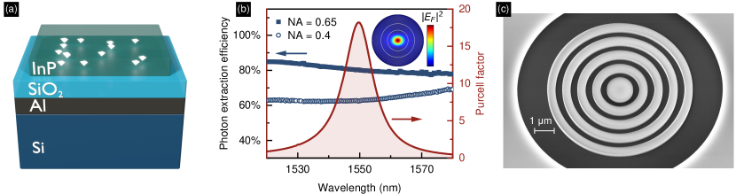
The planar QD structure consists of an epitaxially grown -thick InP slab containing a single layer of InAs QDs. The InP slab is atop a -thick SiO2 layer with a bottom Al mirror bonded to a Si wafer carrier (Fig. 1a, see Methods) [10]. Overall, this geometry enhances the QD emission in the out-of-plane direction by a factor as compared to bulk InP samples, reaching a total photon extraction efficiency of from a single QD for . For QD localization later in the experiment, we structure the top InP layer in a mesh with fields of size separated by -wide ridges (see Methods), where the field edges are used as alignment marks (AMs) for imaging. The fields are furthermore organized in blocks accompanied by InP crosses that allow us to align the electron beam to specific target QDs during the EBL process (see Supplemental Material for the optical microscope image of the sample surface with fabricated cavities).
For the self-assembled Stranski-Krastanov QD epitaxy, we employed the near-critical growth regime in metalorganic vapor-phase epitaxy (MOVPE) [12] (see Supplemental Material) and obtained a QD surface density of corresponding to an average QD separation of . Since QDs exhibit a size, shape, and strain distribution, only a fraction of the QDs have their ground-state optical transition in the C-band. With a bandpass filter, we find on average QDs per field, which translates to an effective QD density of and an average QD separation of .
Design of circular Bragg grating cavities
The CBG geometry is optimized using the modal method (see Supplemental Material) to enhance the cavity figures of merit at , namely the collection efficiency at the first lens and the Purcell factor (). As opposed to other implementations [9], we consider a simplified CBG geometry consisting of a central mesa and only four external rings. According to our calculations, this number is sufficient for high and , providing a smaller footprint and less complexity in the fabrication process. The in-plane cavity dimensions include the central mesa radius of , the grating period of , and the separation between InP rings (air gap) of . For these geometrical parameters, Fig. 1b shows the calculated broadband that amounts to nearly and at for a NA of and , respectively, which is similar to other state-of-the-art CBG designs [13, 14, 15]. The wavelength dependence of the Purcell factor, presented in Fig. 1b, mimics the CBG cavity mode centered at and reaches a maximum value with a quality factor of . The influence of the cavity geometry on the dispersion of and suggests that the cavity grating together with the Al mirror creates a photonic bandgap that governs the -dependence and enhances the emission directionality, while the InP membrane thickness and central mesa diameter crucially affect the center wavelength of the -dependence. A scanning electron microscopy (SEM) image of a fabricated CBG cavity is shown in Fig. 1c.
Optical imaging and QD localization
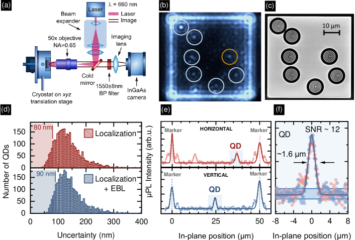
The NIR imaging setup utilizes a wide-field bright microscope configuration as shown in Fig. 2a. The structure with QDs above the Al reflector is mounted in an optical cryostat at movable by a x-y-z stage for targeting fabricated fields that are imaged consecutively. For sample illumination, we use a continuous-wave semiconductor laser diode, spatially shaped with a beam expander, and focused on the backside of a commercially-available microscope objective () with magnification, transmission in the NIR, and working distance. This configuration provides nearly homogeneous surface illumination across a field and high photon collection efficiency. The spatially-distributed QD microphotoluminescence (PL) and scattered light from the field edges (here used as AMs) are collected by the same objective and pass through a cold mirror cutting off the laser light. Finally, the emission is projected onto a thermo-electrically cooled InGaAs-based camera with a chip and a pixel size of . With the magnification lens in front of the camera, the setup has a magnification, enabling the optimal filling of the entire camera chip with a single field (Fig. 2b). The band-pass filter with full-width half-maximum (FWHM) placed in front of the imaging lens selects QDs with emission in the C-band.
Figure 2b shows a representative image of a field recorded with a camera integration time of . The QDs can clearly be recognized as individual bright spots with FWHM (see Fig. 2f and Supplemental Material) and Airy rings around. The square-shaped outline of the field scatters light and is used as AM for QD localization.
The localization of QDs is performed by taking vertical and horizontal cross-sections both crossing at a QD emission spot in the PL intensity map. Each cross-section thus contains the position of the target QD relative to two AMs (Fig. 2e). Gaussian profiles fitted to the QD and the AM signals are subsequently used to determine the QD peak position relative to the AMs. The average signal-to-noise ratio for QD emission spots is , emphasizing the importance of the emission enhancement in the planar structure as compared to bulk InP. We find that for the brightest of all QDs with SNR, the position is fitted with an uncertainty of in 1D and with an uncertainty of the AM position of , resulting in a total uncertainty of QD position in 1D of . In 2D, this translates to accuracy for the QD localization. Finally, taking into account the EBL alignment accuracy of as measured in our previous work [16], we estimate the overall accuracy of 2D CBG placement to . The histograms of QD localization accuracy and overall cavity placement accuracy for all detected spots are shown in Fig. 2d in the upper and lower panel, respectively, and the and levels are marked for reference. Medians for the distributions are slightly larger, and , due to processing of all detected spots, irrespective of their brightness and expected cavity fabrication precision. Details on the localization algorithm, derivation and discussion of the uncertainties, and data on the accuracy of cavity positioning are given in the Supplemental Material. Following the localization of suitable QDs, CBGs are fabricated using EBL with proximity error correction and an optimized inductively coupled plasma-reactive ion etching (ICP-RIE) process (see Methods). The SEM image presented in Fig. 2c is taken from the same field after fabricating the CBG cavities around pre-selected QDs indicated by the circles in Fig. 2b.
Characteristics of the fabricated devices
Process yield
We use a PL setup to quantify the process yield that we define as the ratio between the number of QD-CBG devices with QD emission spectra matching the CBG mode and the number of all CBGs investigated, and we obtain . This value should be compared with the yield that would be obtained in a statistical QD-CBG fabrication process. As we estimate the average number of QDs per field of size to , the probability of covering one of them with the central mesa of diameter is . Some of the QD (inside a CBG) emission spectra are significantly broadened (median linewidth of , see Supplemental Material) as compared to the narrowest recorded linewidth of (identical to the spectrometer resolution). We attribute the broadening to the impact of surface states and point defects caused by the cavity fabrication, effectively resulting in the spectral wandering of the QD emission line [17]. Such defects can as well introduce non-radiative recombination centers in the close vicinity of or even into the QD, quench the optical emission, and effectively reduce the process yield. Using the temperature-dependent PL studies, we make sure that even the broadened emission lines follow the expected Varshni trend, ensuring that these spectral lines can indeed be associated with the QD emission as the temperature dependence of the cavity mode energy is much weaker.
Purcell enhancement
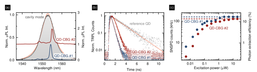
In the following, we discuss the optical properties of two exemplary devices, QD-CBG #1 and QD-CBG #2, each containing a single pre-selected QD coupled to the CBG cavity mode (see Supplemental Material for the properties of a third device QD-CBG #3). Figure 3a shows the narrow QD emission lines overlaid on the cavity mode with , the latter obtained under high power cavity excitation, evidencing good spectral overlap between the cavity mode and the QD emission. We interpret the dominant QD emission lines in both devices as trions (CX), due to their linear intensity dependence on excitation power, and the lack of fine-structure splitting. This is in line with typical spectra for our InAs/InP QDs with preferential CX recombination where the average CX binding energy was measured to be [10].
The coupling between the QD and the CBG cavity is evidenced by the observation of a reduced emission decay time as compared to the decay of QDs in the planar reference structure. For the CX line in QD-CBG #1 and #2 we record decay times of and , respectively (Fig. 3b). To take statistical QD-to-QD fluctuations for the reference decay time into account, we estimate the average decay time of 8 uncoupled QD CX lines and obtain , while the single reference shown in Fig. 3b has a decay time of . Therefore, the measured Purcell factor for QD-CBG #1 is and for QD-CBG #2. Although the obtained Purcell factors are comparable with obtained in the non-deterministic fabrication approach [9], we expect it to be much higher if the QD would perfectly match the cavity mode both spectrally and spatially. However, the expected Purcell factor decays rapidly with the dipole displacement from the cavity center (decreases by half for ), as the fabricated CBG is optimized for a higher-order mode that exhibits electric field minima along the cavity radial direction (see Supplemental Material). Hence, the relatively large total positioning uncertainty for QD-CBGs #1-#3 () and the non-ideal spectral emitter-cavity overlap explain the reduced as compared to the model.
Photon extraction efficiency
We evaluate the photon extraction efficiency by recording the power-dependent PL signal with a superconducting nanowire single-photon detector (SNSPD) in a calibrated optical setup (see Fig. 3c). The setup has a total transmission of (see Supplemental Material). The measured values are corrected by the factor , to account for the detection of secondary photons due to the refilling of QD states [18, 19]. Here, the value is obtained under the excitation power corresponding to saturation of the CX line. Evaluating the CX emission, we obtain an extraction efficiency for QD-CBG #1 and for QD-CBG #2 using an objective with .
Single-photon emission purity
The photon statistics of a quantum light source are of fundamental importance for applications in photonic quantum technologies. In the following, we investigate the single-photon purity of the emission from QD-CBG #2 by analyzing the photon autocorrelation function (cf. Supplemental Material for details on the data analysis and complementary measurements).
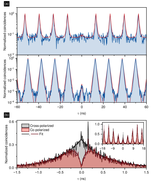
Fig. 4a depicts the measured histograms obtained under pulsed off-resonant excitation at a power and LO-phonon-assisted, quasi-resonant excitation at in the upper and lower panel, respectively. Under off-resonant excitation, the single-photon purity is limited by recapture processes resulting in , where the uncertainty is mainly determined by the background level . From the fit, we determine a decay time of , in good agreement with the spontaneous emission decay time observed in Fig. 3b ().
Under weak quasi-resonant excitation at , the probability for charge-carrier recapture is strongly reduced, resulting in almost negligible background contributions () (Fig. 4a, lower panel) and a fitted value of at . Additionally, we evaluated the raw antibunching value by integrating the raw coincidences around over a full repetition period normalized by the Poisson level of the side peaks. This results in , with the error deduced from the standard deviation of the distribution of counts in the side peaks. As discussed later, this result compares favorably with previous reports on non-deterministically fabricated QD-CBGs.
Photon indistinguishability
Finally, we explore the photon indistinguishability of QD-CBG #2 by Hong-Ou-Mandel (HOM)-type two-photon interference (TPI) experiments [20] (see Methods and Supplemental Material for details on the experimental setup, data analysis, and complementary TPI measurements). The HOM histograms recorded for co- and cross-polarized measurement configurations are presented in Fig. 4b, and were obtained under pulsed quasi-resonant excitation with identical experimental conditions as the measurement presented in the previous section (at ). The data shown in Fig. 4b is not corrected for multi-photon events or contributions from residual laser light.
The HOM histograms feature a characteristic pattern that we analyze following the methodology described in Ref. 21. The reduced area of the central peak in the co-polarized measurement as compared to the maximally distinguishable cross-polarized measurement is a distinct signature of the two-photon coalescence due to a significant degree of photon-indistinguishability. From the width of the central dip we extract a photon coherence time of . The visibility of the TPI is calculated from the ratio of the fitted central peak area in the co- and cross-polarized measurements as . We obtain a TPI visibility of with the accuracy being the propagated fitting errors reflecting the statistics of the experimental data. The temporally post-selected visibility at zero delay time () is , limited only by the system temporal response.
Discussion
The scalable fabrication of active quantum photonic devices operating in the telecom C-band has been a long-standing challenge. This is mainly due to the random size and strain distribution of epitaxially grown QDs causing an inhomogeneous broadening of the emission and difficulties in localizing suitable QDs due to the high electronic noise level of detector arrays sensitive around wavelength. In this work, we present a solution to this problem based on a hybrid sample design. We fabricate an InP layer containing epitaxial QDs on top of a Al reflector placed on a Si wafer carrier. This geometry significantly enhances the photon extraction efficiency from the QDs by a factor enabling the localization of single QDs in a wide-field imaging setup with a thermo-electrically cooled InGaAs camera. For the brightest QDs our setup achieves an imaging SNR and a localization uncertainty of with respect to alignment marks. After final EBL processing, we achieve an overall uncertainty of for fabricating a nano-photonic device around pre-selected QDs. The localization accuracy of our setup is comparable to setups operating in the range ( [22], [23]) where Si-based sensors with four orders of magnitude lower electronic noise can be used. The accuracy in our setup can be further improved by using higher-NA objectives inside the cryostat together with an overall increased microscope magnification, which was reported to reduce the localization accuracy down to [24]. Alternatively, in-situ EBL [25] or photolithography [26] scanning techniques provide a similar accuracy down to , but are comparably slow, require cathodoluminescence signal for QD localization or, in case of photolithography, are not suitable to define reliably sub- features.
To exemplify our approach, we fabricate CBG cavities with a resonance wavelength of around some of the pre-selected QDs. The QD-to-CBG coupling is evidenced by a Purcell factor of , further increasing the single-photon emission rate and final source brightness. Using our approach, we obtain a total process yield of for finding a pre-selected QD spectrally matching the CBG cavity, which is a significant improvement compared to the yield achievable with a random placement approach (). For our QD-CBG device, we measure a photon extraction efficiency of with a objective, which is comparable to previously reported devices probabilistically-fabricated and operating at C-band wavelengths [9].
Our QD-CBG devices feature excellent single-photon emission purities with raw values down to , beating previous records for non-deterministically fabricated QD-CBGs [9], as well as most QDs operating in the C-band [27, 28], while being not yet competitive with the state-of-the-art [29].
Importantly, we report for the first time triggered TPI experiments for InP-based cavity-coupled QDs with emission wavelengths in the telecom C-band, which is crucial for applications in quantum information processing (QIP). We generate indistinguishable photons with a TPI visibility up to and a post-selected value of at zero time delay, setting a new record for QDs emitting in the C-band. Previous results in the C-band were based either on droplet epitaxy InAs/InP QDs in planar structures [30, 31] or InAs QDs grown on GaAs followed by an InGaAs metamorphic buffer, also located in planar structures [32, 33] or embedded in randomly placed CBGs [9].
Further improvement in the photon indistinguishability is of utmost importance for applications in QIP. This is challenged by the strong coupling of QDs to their semiconductor environment via charge and spin noise, both causing QD decoherence [34, 21]. It is thus important to stabilize the QD environment, e. g. via electrical gates. In combination with coherent pumping schemes, such as two-photon resonant excitation, we expect a further improvement of the photon coherence time and hence indistinguishability [35].
Moreover, the InP material system used in our work appears to be advantageous for QD-based quantum photonic devices operating in the C-band and compared to GaAs-based devices. Despite the careful strain engineering involved in the epitaxy of QDs on GaAs [36], the metamorphic buffer complicates the device engineering and QD growth. In contrast, an unstrained InP system is free from threading dislocations that would be a source of dangling bonds causing non-radiative recombination, thus lowering the efficiency [37].
In conclusion, our work opens the route for the scalable fabrication of telecom C-band wavelength quantum photonic devices with QDs delivering flying qubits, i.e. single or entangled photons [38], or acting as a non-linear element for QIP [39].
Improvements in our optical imaging setup will further increase the device yield and positioning accuracy, while the electric control and coherent excitation of QD emitters will further push the achievable photon-indistinguishability.
Methods
Epitaxial growth and fabrication of planar structure with QDs–
The fabrication of the QD-CBG devices starts with the MOVPE growth of low-density Stranski-Krastanov InAs/InP QDs emitting in the C-band [12].
Then, the applied process analogous to the one described in Ref. 10 results in the structure consisting of a thin InP layer with QDs over SiO2 and Al, heterogeneously integrated with a Si carrier wafer using BCB and ready for imaging.
Further details are given in Supplemental Material.
Modeling of the CBG– The QD is modeled as a classical dipole [40], and the numerical simulations of the CBG geometry are performed using a modal method employing a true open boundary condition [41].
See the Supplemental Material for further details.
Deterministic fabrication of QD-CBG devices–
After the PL imaging step, introduced in the Results section and elaborated in Supplemental Material, the CBG cavities are fabricated via e-beam lithography using high-precision alignment based on the InP mark detection in JEOL JBX-9500FSZ e-beam writer.
This step is followed by HBr-based ICP-RIE etching, using CSAR resist and a PECVD-deposited SiNx hard mask.
The calculated design is first scaled and fabricated using a nominally identical heterostructure to investigate the mode energy vs. size dependence and to account for the fabrication imperfections.
Additionally, we experimentally determine the temperature-induced blueshift of the mode energy between a room and low temperature resulting from the contraction of the structure (introducing size and strain changes), as well as from the change of the refractive indices of the layers.
Optical characterization of devices– The structure with QD-CBG devices is held in a helium-flow cryostat allowing for control of the sample temperature in the range of . For our standard PL studies, the structures are optically excited through a microscope objective with or and magnification using or light generated with semiconductor laser diodes. The same objective is used to collect the PL signal and to direct it for spectral analysis into a -focal-length monochromator equipped with a liquid-nitrogen-cooled InGaAs multichannel array detector, providing spatial and spectral resolution of and , respectively.
The photon extraction efficiency and time-resolved PL are measured in the same setup.
Here, QDs are excited by -long pulses with a repetition rate of and a central wavelength of .
At the same time, the second monochromator output port is equipped with the fiber coupling system, transmitting the signal to an NbN-based SNSPD (Scontel) with quantum efficiency in the range and dark counts per second.
A multichannel picosecond event timer (PicoHarp 300 by PicoQuant GmbH) analyzes the single photon counts as a time-to-amplitude converter.
The overall time resolution of the setup is .
Experimental setups, and data on the setup transmission efficiency used for determining the photon extraction efficiency are given in Supplemental Material.
Photon autocorrelation measurements–
For the photon-autocorrelation measurements, QD-CBG devices were optically excited using a Ti:Sapphire (Ti:Sa) laser (Coherent Mira-HP) or a widely tunable ps-pulsed laser system based on an optical parametric oscillator (OPO) (picoEmerald by APE GmbH) with repetition rates of and , respectively.
We use a fiber-coupled bandpass filter () for spectrally selecting the QD emission, followed by a 50:50 fiber beam splitter.
For the off-resonant excitation, we use a microscope objective with and magnification and excite the QD emission with -long pulses at from the Ti:Sa.
The signal is detected with a pair of SNSPDs with and quantum efficiency at .
For the quasi-resonant excitation, we use an aspheric lens () mounted inside a low-vibration closed-cycle cryostat (attoDRY800 by Attocube Systems AG) cooled to .
Here, the OPO-laser is used and adjusted to a pulse length of .
Single photons are detected via SNSPDs with detection efficiency at and timing jitter (complete system temporal response).
The excitation energy was determined in photoluminescence excitation experiments to be ( above the QD emission energy, cf. Supplemental Material), which was also used for following TPI experiments.
Photon-indistinguishability measurements–
In the TPI experiments, an additional delay was introduced between consecutive laser pulses by adding an imbalanced free-space Mach-Zehnder interferometer (MZI) in the excitation path, which was compensated in the HOM setup on the detection side.
Hence, the excitation sequence is composed of pairs of pulses separated by , every corresponding to laser repetition rate.
Free-space waveplates were used to match the polarization for the TPI inside the fiber beam splitter.
The exact polarization was set by using a polarimeter at the beam splitter output in combination with a laser tuned to the QD emission wavelength.
Fine-tuning the relative delay between both MZI arms was used to precisely match the detection and excitation delay, respectively. The contrast of classical Michelson interference of the laser with itself was used for optimization.
See Supplemental Material for the scheme of the experimental setup and the details of the HOM data analysis.
Acknowledgements
The authors acknowledge financial support from the Danish National Research Foundation via the Research Centers of Excellence NanoPhoton (DNRF147) and the Center for Macroscopic Quantum States bigQ (DNRF142).
P. H. was funded by the Polish National Science Center within the Etiuda 8 scholarship (Grant No. 2020/36/T/ST5/00511) and by the European Union under the European Social Fund.
D. A. V. and T. H. acknowledge financial support by the German Federal Ministry of Education and Research (BMBF) via the project “QuSecure” (Grant No. 13N14876) within the funding program Photonic Research Germany, the BMBF joint project “tubLAN Q.0” (Grant No. 16KISQ087K), and by the Einstein Foundation via the Einstein Research Unit “Quantum Devices”.
P. M. acknowledges the financial support from the Polish National Science Center (Grant No. 2020/39/D/ST5/02952).
N. G. acknowledges support from the European Research Council (ERC-CoG “UNITY”, Grant No. 865230), and from the Independent Research Fund Denmark (Grant No. DFF-9041-00046B).
Funding Sources
Danish National Research Foundation: DNRF147, DNRF142;
Polish National Science Center: 2020/36/T/ST5/00511; 2020/39/D/ST5/02952
European Union: European Social Fund;
European Research Council: 865230;
Independent Research Fund Denmark: DFF-9041-00046B
German Federal Ministry of Education and Research: 13N14876, 16KISQ087K;
Einstein Foundation: Einstein Research Unit “Quantum Devices”.
Supplemental Material
The description of device fabrication, numerical simulations, extended data for QD localization algorithm and uncertainty analysis, optical characterization of the devices, evaluation of single-photon purity, and the analysis of the two-photon-interference measurements.
References
- Kimble [2008] H. J. Kimble, “The quantum internet,” Nature 453, 1023–1030 (2008).
- Gisin et al. [2002] N. Gisin, G. Ribordy, W. Tittel, and H. Zbinden, “Quantum cryptography,” Rev. Modern Phys. 74, 145–195 (2002).
- Vajner et al. [2022] D. A. Vajner, L. Rickert, T. Gao, K. Kaymazlar, and T. Heindel, “Quantum communication using semiconductor quantum dots,” Adv. Quantum Technol. 5, 2100116 (2022).
- Serafini, Mancini, and Bose [2006] A. Serafini, S. Mancini, and S. Bose, “Distributed quantum computation via optical fibers,” Phys. Rev. Lett. 96, 010503 (2006).
- Cao et al. [2022] Y. Cao, Y. Zhao, Q. Wang, J. Zhang, S. X. Ng, and L. Hanzo, “The Evolution of Quantum Key Distribution Networks: On the Road to the Qinternet,” IEEE Communications Surveys & Tutorials 24, 839–894 (2022).
- Gazzano et al. [2013] O. Gazzano, S. M. de Vasconcellos, C. Arnold, A. Nowak, E. Galopin, I. Sagnes, L. Lanco, A. Lemaître, and P. Senellart, “Bright solid-state sources of indistinguishable single photons,” Nat. Commun. 4, 1425 (2013).
- Tomm et al. [2021] N. Tomm, A. Javadi, N. O. Antoniadis, D. Najer, M. C. Löbl, A. R. Korsch, R. Schott, S. R. Valentin, A. D. Wieck, A. Ludwig, and R. J. Warburton, “A bright and fast source of coherent single photons,” Nat. Nanotechnol. 16, 399–403 (2021).
- Wang et al. [2016] H. Wang, Z.-C. Duan, Y.-H. Li, S. Chen, J.-P. Li, Y.-M. He, M.-C. Chen, Y. He, X. Ding, C.-Z. Peng, C. Schneider, M. Kamp, S. Höfling, C.-Y. Lu, and J.-W. Pan, “Near-transform-limited single photons from an efficient solid-state quantum emitter,” Phys. Rev. Lett. 116, 213601 (2016).
- Nawrath et al. [2022] C. Nawrath, R. Joos, S. Kolatschek, S. Bauer, P. Pruy, F. Hornung, J. Fischer, J. Huang, P. Vijayan, R. Sittig, M. Jetter, S. L. Portalupi, and P. Michler, “High emission rate from a Purcell-enhanced, triggered source of pure single photons in the telecom C-band,” (2022), arXiv:2207.12898 [quant-ph] .
- Holewa et al. [2022] P. Holewa, A. Sakanas, U. M. Gür, P. Mrowiński, A. Huck, B.-Y. Wang, A. Musiał, K. Yvind, N. Gregersen, M. Syperek, and E. Semenova, “Bright Quantum Dot Single-Photon Emitters at Telecom Bands Heterogeneously Integrated on Si,” ACS Photonics 9, 2273–2279 (2022).
- Liu, Srinivasan, and Liu [2021] S. Liu, K. Srinivasan, and J. Liu, “Nanoscale positioning approaches for integrating single solid-state quantum emitters with photonic nanostructures,” Laser Photonics Rev. 15, 2100223 (2021).
- Berdnikov et al. [2023] Y. Berdnikov, P. Holewa, S. Kadkhodazadeh, J. M. Śmigiel, A. Frąckowiak, A. Sakanas, K. Yvind, M. Syperek, and E. Semenova, “Fine-tunable near-critical Stranski-Krastanov growth of InAs/InP quantum dots,” (2023), arXiv:2301.11008 [cond-mat.mes-hall] .
- Barbiero et al. [2022] A. Barbiero, J. Huwer, J. Skiba-Szymanska, T. Müller, R. M. Stevenson, and A. J. Shields, “Design study for an efficient semiconductor quantum light source operating in the telecom C-band based on an electrically-driven circular Bragg grating,” Opt. Express 30, 10919 (2022).
- Bremer et al. [2022] L. Bremer, C. Jimenez, S. Thiele, K. Weber, T. Huber, S. Rodt, A. Herkommer, S. Burger, S. Höfling, H. Giessen, and S. Reitzenstein, “Numerical optimization of single-mode fiber-coupled single-photon sources based on semiconductor quantum dots,” Opt. Express 30, 15913 (2022).
- Rickert et al. [2023] L. Rickert, F. Betz, M. Plock, S. Burger, and T. Heindel, “High-performance designs for fiber-pigtailed quantum-light sources based on quantum dots in electrically-controlled circular Bragg gratings,” Opt. Express (2023), 10.1364/oe.486060.
- Sakanas et al. [2019] A. Sakanas, E. Semenova, L. Ottaviano, J. Mørk, and K. Yvind, “Comparison of processing-induced deformations of InP bonded to Si determined by e-beam metrology: Direct vs. adhesive bonding,” Microelectron. Eng. 214, 93–99 (2019).
- Liu et al. [2018] J. Liu, K. Konthasinghe, M. Davanço, J. Lawall, V. Anant, V. Verma, R. Mirin, S. W. Nam, J. D. Song, B. Ma, Z. S. Chen, H. Q. Ni, Z. C. Niu, and K. Srinivasan, “Single self-assembled quantum dots in photonic nanostructures: The role of nanofabrication,” Phys. Rev. Applied 9, 064019 (2018).
- Yang et al. [2020] J. Yang, C. Nawrath, R. Keil, R. Joos, X. Zhang, B. Höfer, Y. Chen, M. Zopf, M. Jetter, S. L. Portalupi, F. Ding, P. Michler, and O. G. Schmidt, “Quantum dot-based broadband optical antenna for efficient extraction of single photons in the telecom O-band,” Opt. Express 28, 19457 (2020).
- Kumano et al. [2016] H. Kumano, T. Harada, I. Suemune, H. Nakajima, T. Kuroda, T. Mano, K. Sakoda, S. Odashima, and H. Sasakura, “Stable and efficient collection of single photons emitted from a semiconductor quantum dot into a single-mode optical fiber,” Appl. Phys. Express 9, 032801 (2016).
- Hong, Ou, and Mandel [1987] C. K. Hong, Z. Y. Ou, and L. Mandel, “Measurement of subpicosecond time intervals between two photons by interference,” Phys. Rev. Lett. 59, 2044–2046 (1987).
- Thoma et al. [2016] A. Thoma, P. Schnauber, M. Gschrey, M. Seifried, J. Wolters, J. H. Schulze, A. Strittmatter, S. Rodt, A. Carmele, A. Knorr, T. Heindel, and S. Reitzenstein, “Exploring dephasing of a solid-state quantum emitter via time- and temperature-dependent Hong-Ou-Mandel experiments,” Phys. Rev. Lett. 116, 1–5 (2016).
- Kojima et al. [2013] T. Kojima, K. Kojima, T. Asano, and S. Noda, “Accurate alignment of a photonic crystal nanocavity with an embedded quantum dot based on optical microscopic photoluminescence imaging,” Appl. Phys. Lett. 102, 011110 (2013).
- Sapienza et al. [2015] L. Sapienza, M. Davanço, A. Badolato, and K. Srinivasan, “Nanoscale optical positioning of single quantum dots for bright and pure single-photon emission,” Nat. Commun. 6, 7833 (2015).
- Liu et al. [2017] J. Liu, M. I. Davanço, L. Sapienza, K. Konthasinghe, J. V. D. M. Cardoso, J. D. Song, A. Badolato, and K. Srinivasan, “Cryogenic photoluminescence imaging system for nanoscale positioning of single quantum emitters,” Rev. Sci. Instrum. 88, 023116 (2017).
- Gschrey et al. [2015] M. Gschrey, A. Thoma, P. Schnauber, M. Seifried, R. Schmidt, B. Wohlfeil, L. Krüger, J.-H. Schulze, T. Heindel, S. Burger, F. Schmidt, A. Strittmatter, S. Rodt, and S. Reitzenstein, “Highly indistinguishable photons from deterministic quantum-dot microlenses utilizing three-dimensional in situ electron-beam lithography,” Nat. Commun. 6, 7662 (2015).
- Dousse et al. [2008] A. Dousse, L. Lanco, J. Suffczyński, E. Semenova, A. Miard, A. Lemaître, I. Sagnes, C. Roblin, J. Bloch, and P. Senellart, “Controlled light-matter coupling for a single quantum dot embedded in a pillar microcavity using far-field optical lithography,” Phys. Rev. Lett. 101, 30–33 (2008).
- Takemoto et al. [2015] K. Takemoto, Y. Nambu, T. Miyazawa, Y. Sakuma, T. Yamamoto, S. Yorozu, and Y. Arakawa, “Quantum key distribution over 120 km using ultrahigh purity single-photon source and superconducting single-photon detectors,” Sci. Rep. 5, 14383 (2015).
- Zeuner et al. [2021] K. D. Zeuner, K. D. Jöns, L. Schweickert, C. R. Hedlund, C. N. Lobato, T. Lettner, K. Wang, S. Gyger, E. Schöll, S. Steinhauer, M. Hammar, and V. Zwiller, “On-Demand Generation of Entangled Photon Pairs in the Telecom C-Band with InAs Quantum Dots,” ACS Photonics 8, 2337–2344 (2021).
- Miyazawa et al. [2016] T. Miyazawa, K. Takemoto, Y. Nambu, S. Miki, T. Yamashita, H. Terai, M. Fujiwara, M. Sasaki, Y. Sakuma, M. Takatsu, T. Yamamoto, and Y. Arakawa, “Single-photon emission at 1.5 m from an InAs/InP quantum dot with highly suppressed multi-photon emission probabilities,” Appl. Phys. Lett. 109, 132106 (2016).
- Anderson et al. [2021] M. Anderson, T. Müller, J. Skiba-Szymanska, A. B. Krysa, J. Huwer, R. M. Stevenson, J. Heffernan, D. A. Ritchie, and A. J. Shields, “Coherence in single photon emission from droplet epitaxy and Stranski–Krastanov quantum dots in the telecom C-band,” Appl. Phys. Lett. 118, 014003 (2021).
- Wells et al. [2022] L. Wells, T. Müller, R. M. Stevenson, J. Skiba-Szymanska, D. A. Ritchie, and A. J. Shields, “Coherent light scattering from a telecom C-band quantum dot,” (2022), arXiv:2205.07997 [quant-ph] .
- Nawrath et al. [2019] C. Nawrath, F. Olbrich, M. Paul, S. L. Portalupi, M. Jetter, and P. Michler, “Coherence and indistinguishability of highly pure single photons from non-resonantly and resonantly excited telecom C-band quantum dots,” Appl. Phys. Lett. 115, 023103 (2019).
- Nawrath et al. [2021] C. Nawrath, H. Vural, J. Fischer, R. Schaber, S. L. Portalupi, M. Jetter, and P. Michler, “Resonance fluorescence of single In(Ga)As quantum dots emitting in the telecom C-band,” Appl. Phys. Lett. 118, 244002 (2021).
- Kuhlmann et al. [2013] A. V. Kuhlmann, J. Houel, A. Ludwig, L. Greuter, D. Reuter, A. D. Wieck, M. Poggio, and R. J. Warburton, “Charge noise and spin noise in a semiconductor quantum device,” Nature Physics 9, 570–575 (2013).
- Reigue, Hostein, and Voliotis [2019] A. Reigue, R. Hostein, and V. Voliotis, “Resonance fluorescence of a single semiconductor quantum dot: the impact of a fluctuating electrostatic environment,” Semicond. Sci. Technol. 34, 113001 (2019).
- Sittig et al. [2022] R. Sittig, C. Nawrath, S. Kolatschek, S. Bauer, R. Schaber, J. Huang, P. Vijayan, P. Pruy, S. L. Portalupi, M. Jetter, and P. Michler, “Thin-film InGaAs metamorphic buffer for telecom C-band InAs quantum dots and optical resonators on GaAs platform,” Nanophotonics 11, 1109–1116 (2022).
- Seravalli et al. [2011] L. Seravalli, G. Trevisi, P. Frigeri, D. Rivas, G. Muñoz-Matutano, I. Suárez, B. Alén, J. Canet-Ferrer, and J. P. Martínez-Pastor, “Single quantum dot emission at telecom wavelengths from metamorphic InAs/InGaAs nanostructures grown on GaAs substrates,” Appl. Phys. Lett. 98, 173112 (2011).
- Lu and Pan [2021] C.-Y. Lu and J.-W. Pan, “Quantum-dot single-photon sources for the quantum internet,” Nat. Nanotechnol. 16, 1294–1296 (2021).
- Javadi et al. [2015] A. Javadi, I. Söllner, M. Arcari, S. L. Hansen, L. Midolo, S. Mahmoodian, G. Kiršanskė, T. Pregnolato, E. H. Lee, J. D. Song, S. Stobbe, and P. Lodahl, “Single-photon non-linear optics with a quantum dot in a waveguide,” Nat. Commun. 6, 8655 (2015).
- Novotny and Hecht [2012] L. Novotny and B. Hecht, Principles of Nano-Optics, 2nd ed. (Cambridge University Press, 2012).
- Gür et al. [2021] U. M. Gür, S. Arslanagić, M. Mattes, and N. Gregersen, “Open-geometry modal method based on transverse electric and transverse magnetic mode expansion for orthogonal curvilinear coordinates,” Phys. Rev. E 103, 033301 (2021).