Robustness of momentum-indirect interlayer excitons in MoS2/WSe2 heterostructure against charge carrier doping
ICFO-Institut de Ciencies Fotoniques, The Barcelona Institute of Science and Technology, Castelldefels (Barcelona) 08860, Spain
School of Physics and Engineering, ITMO University, 197101 Saint Petersburg, Russia
Department Physik, Friedrich-Alexander-Universität Erlangen-Nürnberg, Staudtstraße 7, 91058 Erlangen, Germany
II. Physikalisches Institut, Universität zu Köln, Zülpicher Straße 77, 50937 Köln, Germany
Institut für Festkörperelektronik, Technische Universität Wien, Gußhausstraße 25-25a, 1040 Wien, Austria
Faculty of Physics, Warsaw University of Technology, 00-662 Warsaw, Poland
Elettra-Sincrotrone Trieste S.C.p.A., Basovizza, 34149 Trieste, Italy
Department of Chemical Sciences, University of Padova, Via F. Marzolo 1, 35131 Padova, Italy
Synchrotron SOLEIL, Université Paris-Saclay, L’Orme des Merisiers Saint-Aubin, Gif sur Yvette, France
Abstract
Monolayer transition-metal dichalcogenide (TMD) semiconductors exhibit strong excitonic effects and hold promise for optical and optoelectronic applications. Yet, electron doping of TMDs leads to the conversion of neutral excitons into negative trions, which recombine predominantly non-radiatively at room temperature. As a result, the photoluminescence (PL) intensity is quenched. Here we study the optical and electronic properties of a MoS2/WSe2 heterostructure as a function of chemical doping by Cs atoms performed under ultra-high vacuum conditions. By PL measurements we identify two interlayer excitons and assign them to the momentum-indirect Q- and K- transitions. The energies of these excitons are in a very good agreement with ab initio calculations. We find that the Q- interlayer exciton is robust to the electron doping and is present at room temperature even at a high charge carrier concentration ( 1013 cm-2). Submicrometer angle-resolved photoemission spectroscopy (-ARPES) reveals charge transfer from deposited Cs adatoms to both the upper MoS2 and the lower WSe2 monolayer without changing the band alignment. This leads to a small ( 10 meV) energy shift of interlayer excitons. Robustness of the momentum-indirect interlayer exciton to charge doping opens up an opportunity of using TMD heterostructures in light-emitting devices that can work at room temperature at high densities of charge carriers.
Introduction
Monolayer transition metal dichalcogenides (TMDs) are direct band gap semiconductors with multi-valley electronic band structure and strong light-matter coupling. These properties give rise to a variety of electron-hole pair excitations (excitons) that are stable at room temperature. [1] When monolayer TMDs are stacked in van der Waals heterostructures with type-II band alignment, electrons and holes reside in different layers and interlayer excitons (ILEs) emerge. Such ILEs demonstrate extremely long lifetime, large valley polarization and coherence, necessary for valleytronics applications. [2, 3, 4] It was demonstrated that application of external electric fields provides control over properties of ILEs: their intensity and photon energy, [2] valley polarisation, [3, 5] and flux. [6] Such versatile tunability of ILEs makes TMDs heterostructures promising for designing optoelectronic devices such as light-emitting diodes (LEDs), solar cells, photodetectors, energy conversion and storage devices. First, an ILE in MoS2/WSe2 heterostructures fabricated on SiO2 substrates was observed with light emission at around 1.6 eV, [7, 8, 6] and the electrical control of its diffusion in a sample encapsulated between hexagonal boron nitride (hBN) layers was also demonstrated. [6] Experimental data and calculations suggest that this ILE is momentum-indirect, i.e. an electron in MoS2 and a hole in WSe2 have different wavevectors. [8] It was proposed that this ILE consists of an electron residing in the K valley of MoS2 and a hole residing in the valley of WSe2. [8] Further, a momentum-direct ILE, coupling the K valleys of MoS2 and WSe2, was found in MoS2/WSe2 heterostructure at around 1 eV. [9] Interestingly, in a very similar system – hBN-encapsulated MoS2/WS2, two momentum-indirect ILEs were observed. [10] These ILEs are associated with two conduction band (CB) valleys of MoS2 located in the K and Q points and the valence band (VB) valley of WS2 at the point. [10] The hBN encapsulation plays an important role in this finding. For example, for a non-encapsulated MoS2/WS2 heterostructure on SiO2, the contribution of two momentum-indirect ILEs cannot be well resolved. [11] These results suggest further investigation of the MoS2/WSe2 system, in which two types of momentum-indirect ILEs can be also present.
Besides the origin of ILEs in TMD heterostructures, another open question is the impact of charge doping on the ILE emission. This is an important question not only from a fundamental but also from an applied point of view. For devices that require both light emission and charge transport, it is important to maintain the radiative efficiency at an increased charge carrier densities. For example, conductivity and the charge carrier mobility in TMDs can be increased by charge doping. [12] However, increased charge carrier concentration in TMD monolayers leads to the conversion of neutral excitons into trions, which have long radiative and short non-radiative lifetimes. [13] In the case of electron doping, negative trions, composed of two electrons and one hole, will appear. Here, the main mechanism responsible for non-radiative recombination is the Auger process, where the energy of electron–hole recombination is transferred to the third particle (i.e. an electron in negative trions). [14, 13, 15] Thus, Auger recombination dramatically decreases the PL quantum yield, which complicates the use of TMDs as optical active elements at a high concentration of charge carriers. Nevertheless, the impact of electron doping on PL of momentum-indirect ILEs involving different valleys in CB might be different. To answer these questions, we explore a high-quality MoS2/WSe2/hBN van der Waals heterostructure and find two momentum-indirect ILEs. To understand the origin of these ILEs, we perform ab initio calculations of optical transitions in MoS2/WSe2 system. We investigate the effect of electron doping on the electronic and optical properties of the MoS2/WSe2 heterostructure using the deposition of Cs atoms in situ. Ultra-high-vacuum (UHV) PL spectroscopy reveals that the Q- exciton is robust to the electron doping and is emitting light even at high charge carrier concentration ( 1013 cm-2) at room temperature. Using the spatially-resolved angle-resolved photoemission spectroscopy with sub-micron spot (-ARPES), we find that the deposition of Cs has a minor impact on the VB alignment in MoS2/WSe2 heterostructure. This is due to the intercalation of Cs in the van der Waals gap, which leads to equal charge distribution between the TMD monolayers. This explains the minor shift of ILEs in the MoS2/WSe2 system upon Cs doping. The robustness of momentum-indirect ILEs to the charge doping paves the way towards the design of novel optoelectronic devices based on TMD heterostructures with combined effective light emission and improved charge transport properties at high charge carrier concentrations.
Sample fabrication and characterization
PL and -ARPES studies were performed on similar samples fabricated by the deterministic transfer technique. [16] The MoS2/WSe2 heterobilayers were assembled layer by layer on hBN flakes placed on epitaxial bilayer graphene grown on SiC. The advantage of such a substrate is that hBN is an atomically flat and pure insulator (in contrast to SiO2), while graphene provides the electrical conductivity (through the TMD edges lying outside the hBN flake), necessary for -ARPES measurements. The hBN flake also ensures the absence of charge transfer between the TMD heterostructure and graphene in PL measurements. To minimize organic residues, we exfoliated monolayer TMDs on ultraviolet-ozone cleaned polydimethylsiloxane (PDMS) stamps. [17] Post-transfer thermal annealing of the TMDs heterostructure is an important step to provide strong interlayer coupling. [18] Our samples were annealed in UHV at 250 ∘C for 3 hours.For further details see Supplementary Information S1.
1.0
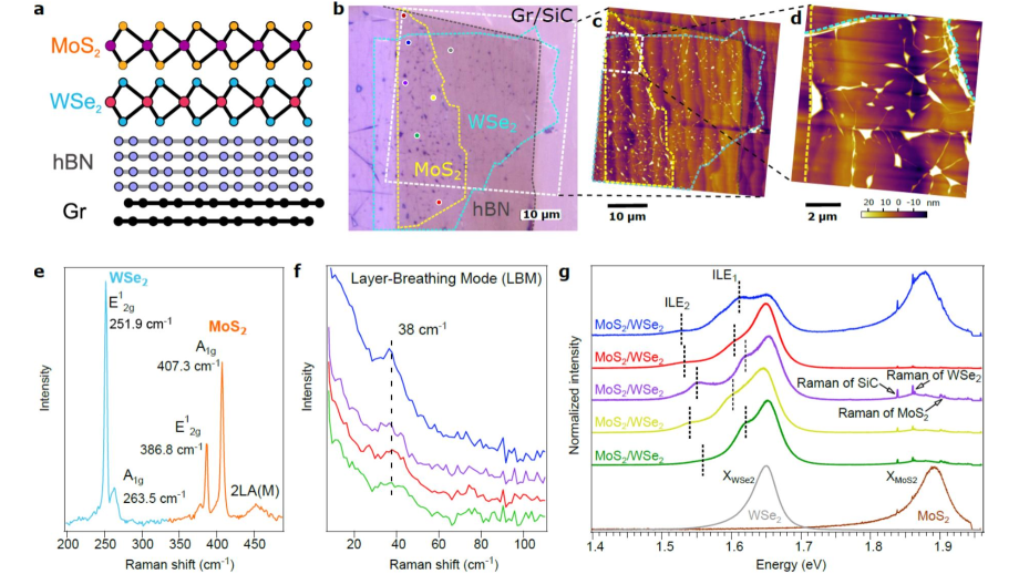
Fig. 1 (a) illustrates the MoS2/WSe2 heterostructure on hBN on bilayer graphene/SiC. The optical image of the sample with indicated edges of the MoS2 and WSe2 monolayers is shown in Fig. 1 (b). The monolayers were not perfectly aligned. The twist angle between TMD monolayers was varying within 5∘ as determined using the second-harmonic generation (SHG) measurements (see Supplementary Information, Fig. S2). Our heterostructures are quite large – several tens of microns, which allows us to probe and compare different points on the sample. The atomic force microscopy (AFM) measurements shown in Fig. 1 (c, d) reveal the surface topography. The exfoliated flakes follow the characteristic atomically flat terraces of hexagonal SiC(0001) with epitaxial bilayer graphene. UHV annealing leads to the aggregation of contaminants trapped between the layers into the bubbles (or blisters). These bubbles are also visible in optical microscope and we select the bubble-free regions to measure Raman and PL spectra with the laser spot of 1 m. AFM reveals the height of MoS2/WSe2 heterobilayer of 1.5 nm (Supplementary information, Fig. S3), indicating the absence of organic residues at the interface and the surface. [17]
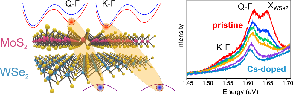
Fig. 1 (e) shows the typical Raman modes of MoS2 and WSe2 in the heterostructure region (532 nm laser). The clean interface provides strong interaction between TMD monolayers. Indeed, in Raman spectra measured with a low wavenumber filter (633 nm laser) we observe layer-breathing mode (LBM), Fig. 1 (f). This mode arises from the out-of-plane vibration of two monolayers when they are in close proximity. The frequency of the LBM mode (38 cm-1) is comparable to that measured on a heterostructure fabricated from chemically grown TMDs on SiO2 (35 cm-1). [19] The small difference in frequency might be related to the different substrates or slightly different twist angles. When the laser spot is directed into the bubble, the LBM mode is absent due to weak interlayer coupling in these areas, the signal from the individual monolayers dominates the PL spectra and the ILE peaks, discussed below, are vanishing. These facts allow us to exclude the contribution of bubbles to the PL spectra. Fig. 1 (g) shows the PL spectra measured at room temperature in air in different bubble-free regions of the sample. One can identify the PL peak of MoS2 at 1.88 eV. This peak is composed of intralayer neutral exciton and negatively charged trion (which manifests itself in the asymmetry of the PL peak towards lower energies). [20, 21] The PL of MoS2 is suppressed in most of the assessed points due to the interlayer charge transfer in a type-II TMD heterostructure. [22, 7, 2] The PL peak at 1.65 eV is the intralayer exciton of WSe2, later referred to as XWSe2. The energy of the momentum-direct K-K exciton in MoS2/WSe2 system is in the infrared range. [9] Other multi-particle exciton complexes, which may appear energetically below the XWSe2, such as trions, biexcitons, defect bound excitons, moiré excitons can be observed only at cryogenic temperatures. [23, 24, 25, 26, 27, 28, 29] Consequently, the PL peaks that are observed only in the heterostructure region at room temperature and whose energy is just below the XWSe2 peak should be attributed to the momentum-indirect ILEs. In contrast to the previous studies, revealing a single ILE peak at 1.6 eV in the MoS2/WSe2 heterostructures on SiO2, [8, 6, 30] we clearly observe two peaks – at 1.61 eV and at 1.55 eV, and denote them as ILE1 and ILE2, respectively. The energies and intensities of the two ILEs peaks slightly vary from point to point and from sample to sample (see Supplementary Information, Fig. S1). This can be attributed to the variations of interlayer twist angle, interlayer spacing and doping.
In situ chemical doping and UHV PL studies
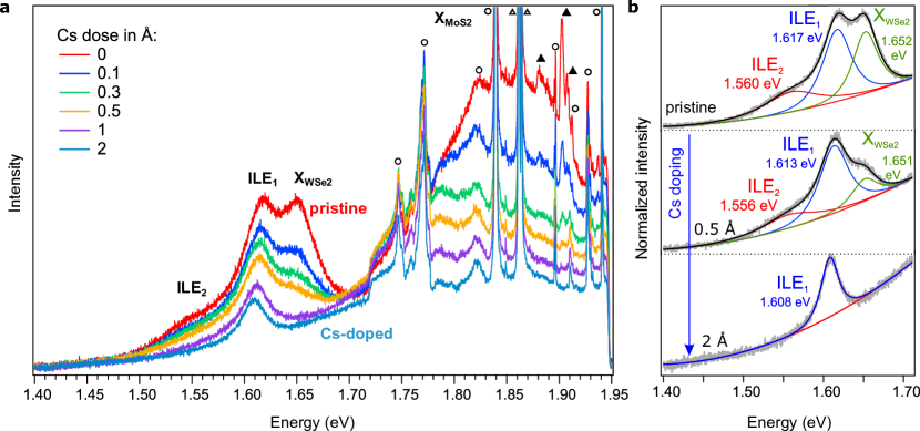
To avoid the effect of air adsorbates (e.g. water molecules, oxygen, hydrocarbons) and to investigate the impact of chemical doping on intrinsic optical properties of MoS2/WSe2 system, we performed PL studies in UHV conditions. For this we used a unique UHV optical setup for PL and Raman studies. [31, 32, 33, 34] Fig. 2 (a) shows the evolution of the UHV PL spectra of the sample upon deposition of Cs. The Cs dose was calibrated using a quartz crystal microbalance. The measurements show that intralayer excitons (XMoS2 and XWSe2) and the interlayer exciton ILE2 are suppressed as the Cs dose increases. The PL of excitons is mainly suppressed due to their conversion to negative trions [20, 35] via electron donation by Cs atoms with the subsequent non-radiative recombination of trions through Auger processes. [14, 13, 15] Moreover, doping increases the dielectric screening of electron-hole Coulomb interaction, and hence reduces the binding energy and the oscillator strength of excitons, [36] which in turn lowers the radiative decay rate. In addition, in case of intercalation of Cs into the van der Waals gap, the interlayer distance will be increased and, consequently, the PL intensity will be reduced. After deposition of 1 Å of Cs one can see almost no signal from XMoS2, XWSe2 and ILE2 peaks (purple spectrum in Fig. 2 (a)). At the same time, the intensity of the ILE1 peak is relatively large. Even after increasing the Cs dose to 2 Å, the ILE1 peak remains clearly visible, while its intensity is reduced by a factor of 3 (light blue spectrum in Fig. 2(a)). blue The Cs dosage above 2 Å has much less effect on PL spectra, and we did not observe complete suppression of the ILE1 peak. Fig. 2 (b) shows the fits of the PL spectra in the pristine and Cs-doped heterostructure. The energies of PL peaks are identified. The full width at half-maximum (FWHM) of these peaks are 19, 21 and 40 meV for XWSe2, ILE1 and ILE2, correspondingly. Such narrow emission lines at room temperature indicate the high quality of our samples. [37] This is due to the atomically flat hBN substrate without charge impurities and the absence of unintended functionalization by air adsorbates in UHV conditions. Further evidence of high-quality samples comes from the well-resolved electronic bands in -ARPES spectra shown below, since ARPES is a surface-sensitive technique requiring atomically-clean surfaces and interfaces. Interestingly, upon doping, the ILE1 peak becomes even narrower (lower spectrum in Fig. 2 (b)). The FWHM of ILE1 is 13 meV at the maximum doping level. This suggests that there is no broadening of ILEs due to the inhomogeneous doping or exciton scattering.
1.0
Energies of interlayer excitons
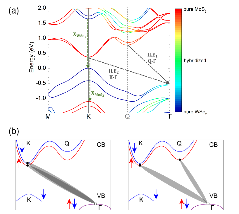
To understand the nature of the observed ILEs, we compare the energy position of PL peaks with calculations. The energies of the XMoS2, XWSe2 and ILE2 peaks (1.9 eV and 1.65 eV, and 1.55 eV, correspondingly) agree very well with the reported ab initio calculations of intralayer MoS2 and WSe2 K-K transitions and interlayer K- transition, respectively. [9] Previously, [8] for the heterostructures on SiO2 substrate, the ILE2 peak was not observed, and the K- transition was assigned to the peak at 1.6 eV, which we designated as ILE1.
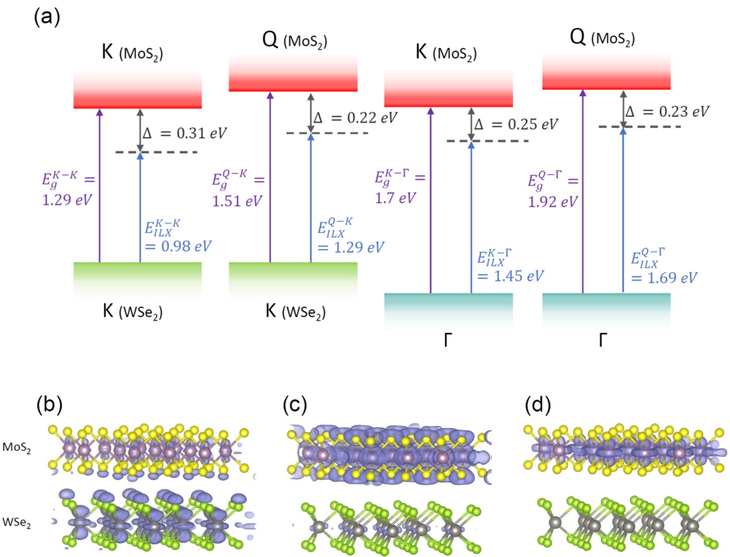
To shed further light on the nature of ILE1 and ILE2, we performed additional theoretical calculations to estimate the binding energies of the momentum-indirect K-, Q- and Q-K excitons combining the solution of the Bethe-Salpeter Equation (BSE) with density functional theory calculations. We refer to the method section and the Supplementary Information for details on the computational approach. Figure 3 (a) shows the obtained electronic band gaps, exciton binding energies and predicted excitonic peak positions of the direct K-K and the three candidate indirect transitions.
For the interlayer K-K transitions, we predict a binding energy and a peak position of 310 meV and 1 eV, respectively, in good agreement with experiments [9] and previous theoretical works. [38, 39] According to our calculations, a Q-K exciton with binding energy 220 meV should appear at an energy of about 1.3 eV, however, to the best of our knowledge, it has not been observed experimentally so far. K- and Q- excitons involve the same hole valley at , but different electronic valleys with different corresponding effective masses. Therefore, the binding energies for the K- and Q- excitons may also be different. Nevertheless, we find very similar binding energies for these excitons (Fig. 3 (a)), and the difference in PL peak positions is determined by the difference in electronic band gaps, such that . This would suggest that ILE2 indeed should be assigned to a K- exciton, while ILE1 is the Q- transition. The energies of the ILE1 and ILE2 peaks (1.61 eV and 1.55 eV) are very close to the calculated values of = 1.69 eV and = 1.45 eV, correspondingly. We note that our DFT calculations likely overestimate the energy difference between the K and Q conduction band minima compared to more sophisticated GW calculations, as observed in lattice-matched MoSe2/WSe2 heterostructures. [39]
According to Fermi’s golden rule, the exciton PL intensity is proportional to the square of the transition matrix element, which, in turn, depends on the overlap between electron and hole wave functions. Momentum-indirect ILEs in type-II TMD heterostructures involve strongly hybridized valleys with large interlayer orbital overlap, and therefore, have significant PL intensity. [8, 10, 11] To compare the Q- and K- ILEs, we should have to look at the wavefunctions of electrons in Q and K valleys of MoS2 and a hole in valley of WSe2. Fig. 3 (b)-(d) demonstrates a certain delocalization of an electron in Q (panel (c)) and a hole in (panel (b)), while this delocalization is completely absent for electrons in the K points of the sublayers (panel (d) for the MoS2 K point). The reason for this is that both Q and valleys in the MoS2/WSe2 heterostructure are hybridized, as shown by the color code in Fig. 4 (a). This hybridization is possible thanks to the energy overlap of MoS2 and WSe2 orbitals in the valley of VB and the Q valley of CB (see Supplementary Information, Fig. S5 (b)). Moreover, the corresponding MoS2 and WSe2 orbitals have similar character – predominantly out-of-plane (d) in VB -valley and mixed in-plane (d and dxy) and out-of-plane in CB Q-valley .[40, 41, 42, 43] The increased electron-hole wavefunction overlap for the Q- transition might explain the brightness of the ILE1 peak in PL spectra compared to the weaker intensity of ILE2 (corresponding electron-hole wavefunction overlap for the K- transition).
1.0
Let us discuss the difference between two momentum-indirect interlayer exciton Q- and K- with respect to the response to electron doping. Upon doping, donated electrons first populate the CB minimum, which is located in the K valley of MoS2. The Q valley gets populated only at charge carrier density larger than 2 – 6 1013 cm-2. [44, 45] As will be seen from our -ARPES data shown below, we reach the electron densities when only the K valley gets populated. Additional charge carriers at the K valley lead to the conversion of K- interlayer excitons (ILE2) into the trions with two electrons in the K (and/or K’) valley and a hole in the valley. Let us denote them as KK- trions. As discussed above, the exciton-to-trion conversion and subsequent non-radiative recombination of trions is the most common mechanism of exciton suppression in TMDs upon charge carrier doping. Fig. 4 (b) illustrates the formation of KK- and QK- trions upon electron doping. For simplicity, we show only the KK- singlet trion, but there also should be a KK’- trion and the respective triplet variants with very similar energies, which might appear upon doping. A negative trion can be considered as two excitons sharing the same hole. That is, the QK- trion having two electrons in the Q and K valleys is the combination of Q- and K- excitons. Our calculations demonstrate that the K- ILE has a lower energy than the Q- ILE. Therefore, the KK- trion should also have a lower energy than the QK- trion. Since trions are fermionic states following the Pauli exclusion principle, the lowest energy ground state corresponding to the KK- trion will be populated first. As a result, the Q- excitons are more stable to the conversion into trions than the K- excitons, and, therefore, are more resistant to electron doping. This confirms the experimentally observed stability of the ILE1 peak in the Fig. 2.
1.0
The band alignment and -ARPES studies
An important question is the change of ILEs energy upon doping. Deposition of alkali metals on the surface of van der Waals layered materials usually leads to the strong out-of-plane potential difference (Stark effect), with the topmost layers being much more heavily doped than the bottom layers. [46, 47, 48] If Cs atoms were resting on top of the MoS2/WSe2 heterostructure, the top MoS2 monolayer would be much more doped than the bottom WSe2 monolayer. This would lead to a strong modification of the band alignment, which, in turn, would result in a significant change of the ILEs energy. Our data in Fig. 2 show that the final doping level causes a shift of the ILE1 peak by only 10 meV. The change in carrier concentration also affects the exciton binding energy and the quasiparticle band gap. Nevertheless, these two renormalization effects usually counteract each other, and the total change in optical band gap is minor. [49, 50] Therefore, small changes in the ILEs energy suggest that the band alignment in the MoS2/WSe2 heterostructure should not be strongly affected by Cs doping. To understand this behaviour, we investigate our system by -ARPES.
1.0
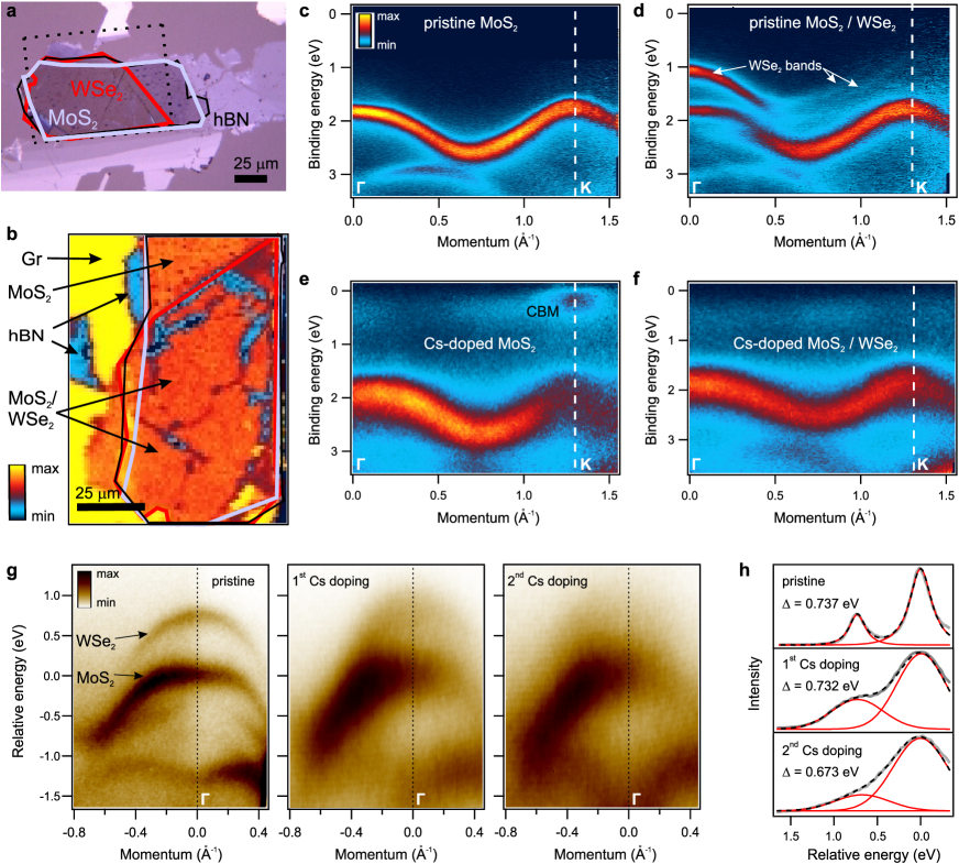
In our experiments we compare MoS2 monolayer and MoS2/WSe2 heterostructure doped by an identical amount of Cs. Fig. 5 summarizes the -ARPES data. The optical image of aligned MoS2/WSe2 heterostructure on an hBN flake on bilayer graphene/SiC used for the -ARPES studies is shown in Fig. 5 (a). The scanning photoemission microscopy (SPEM) image allows identification of the sample location, see Fig. 5 (b). The SPEM image visualizes the integrated photoemission intensity around the K point of MoS2 and WSe2. Figs. 5 (c) and (d) show the energy band structure of the monolayer MoS2 and the MoS2/WSe2 heterostructure measured by -ARPES on the corresponding sample regions. In the heterostructure region (Fig. 5 (d)), in addition to the MoS2 bands one can see bands of WSe2 indicated by the arrows. Specifically, a WSe2 band appears around the point and two spin-split bands appear with vanishing intensities as the K point is approached. In the heterostructure, the WSe2 states at the point are more dispersing as compared to the states in monolayer WSe2, where the topmost band at the point is almost flat (see Supplementary Information, Fig. S3). This is the result of interlayer hybridization with MoS2 states, also predicted by our calculations (Fig. 3 (b)). Figs. 5 (e) and (f) demonstrate corresponding spectra after deposition of 2 Å of Cs adatoms on the sample. The monolayer MoS2 becomes degenerately doped, as we observe the CB states corresponding to the K valley below the Fermi level, Fig. 5 (e). This suggests a doping level of 1013 electrons per cm2. [34] Further deposition of Cs did not result in the appearance of a Q point below the Fermi level, supporting the fact that the PL signal from the Q- ILE was not completely suppressed (Fig. 2), and we are close the maximum possible Cs doping of our system. At the same time, the MoS2/WSe2 heterostructure is not turned into a metal, since its CB does not cross the Fermi level, Fig. 5 (f). This implies that in the heterostructure the upper MoS2 layer is less doped compared to the monolayer sample, and a significant amount of charge is transferred to the lower WSe2 layer. We then performed an experiment with step-by-step deposition of Cs. The obtained high-resolution -ARPES spectra are shown in Fig. 5 (g), and the corresponding energy distribution curves (EDCs) at the point are shown in Fig. 5 (h). After the first Cs dose ( 1 Å), the MoS2 and WSe2 bands have large energy broadening, but the energy distance between them (indicated as in Fig. 5 h) is not changed. The second deposition of the same Cs dose leads to the minor reduction of the . Therefore, we can conclude that the Cs doping has a minor impact on the relative energy positions of MoS2 and WSe2 bands in the heterostructure. This suggests an equal charge doping of MoS2 and WSe2 monolayers, which can occur when Cs atoms are intercalated into the interlayer van der Waals gap. This is also supported by our X-ray photoemission spectroscopy (XPS) data (see Supplementary Information, Fig. S6). A similar behaviour was previously observed by ARPES during the deposition of potassium onto the surface of a bulk MoS2 crystal. [51] Previous DFT calculations also supported that intercalation of deposited alkali metals into the van der Waals gap between the topmost TMD monolayers is much more energetically favorable than the adsorbtion on the surface. [51]
It should be noted that in addition to electron doping, which can be implemented in devices, other effects also take place during chemical doping. First, the presence of positive Cs ions can contribute to exciton scattering. [52] Second, intercalation of alkali metals leads to an increased interlayer distance. Nevertheless, our experimental data suggest that Cs intercalation does not completely suppress the Q- exciton (as occurs in the case of other excitons): its intensity is reduced by 3 times at largest Cs dose of 2 Å (Fig. 2). Concerning the energy position of Q- exciton peak, theory predicts that the increase of interlayer distance from 0.6 nm to 1 nm should reduce the ILE binding energy in MoS2/WSe2 heterostructure by about 15 meV. [53] This is a small change compared to the two competing factors – the band gap renormalization and the reduction in exciton binding energy due to doping, [34] and is comparable with changes that we observe in our data, were the final doping level causes a shift of the ILE1 peak by only 10 meV.
Conclusions
In conclusion, we fabricated high-quality MoS2/WSe2 heterostructures on hBN/graphene/SiC, and characterize their optoelectronic properties and the effect of chemical doping using combination of UHV PL and -ARPES techniques. Our PL spectra revealed two interlayer excitons, the energies of which agree very well with our ab initio calculations of momentum-indirect K- and Q- optical transitions. The relatively high intensity of the Q- ILE is ascribed to the significan overlap of both electron and hole wave-functions of the hybridized Q and valleys. To investigate the effect of chemical doping on the ILEs, we performed deposition of Cs atoms onto the MoS2/WSe2 system. Room-temperature UHV PL measurements reveal that electron doping induced by Cs leads to the suppression of the emission from both WSe2 and MoS2 intralayer excitons and the K- interlayer exciton. In contrast, PL from Q- interlayer exciton is robust to chemical doping, and is preserved even at high electron concentration ( 1013 cm-2). We attribute this to the stability of Q- ILE to the conversion into trions, which recombine non-radiatively at room temperature. Further insight into the interplay between radiative and non-radiative relaxation channels in chemically doped TMD heterostructures can be provided by time-resolved PL measurements. With -ARPES we found that upon Cs doping the electronic band alignment is almost not changed. This suggests equal charge doping of both monolayers and intercalation of Cs in the interlayer gap. Two doping-induced effects, quasiparticle band gap renormalization and the reduction of exciton binding energy due to the increased screening, counteract each other. As a result, the energy shift of Q- interlayer exciton upon doping is only 10 meV. The robustness of momentum-indirect interlayer excitons creates a new playground for optical studies of doped TMD heterostructures. This also opens an opportunity to use TMDs in light-emitting devices at a high concentration of charge carriers at room temperature.
Methods
0.1 Fabrication of heterostructures
MoS2/WSe2/hBN heterostructures were fabricated on epitaxial bilayer graphene on silicon carbide (SiC). Using bilayer graphene on SiC as a substrate allows us to perform both UHV PL and -ARPES studies. We exfoliated MoS2 and WSe2 monolayers and hBN flakes onto viscoelastic PDMS stamps. [16] The PDMS stamps prior to exfoliation were cleaned with a UV-lamp to minimize organic residues from polymers. [17] The whole cleaning process took 15 minutes. The crystallographic axis (zigzag or armchair) of TMD monolayers on PDMS stamps was determined using the SHG measurements. Then we used a transfer system to create heterostructures layer by layer. First, we’ve transferred a thin (few tens of nm) hBN flake to the substrate by a PDMS clean stamp. Next, a WSe2 monolayer was placed on hBN at a temperature of 60∘C. After that, we align the bottom WSe2 layer on substrate with the PDMS stamp on which MoS2 is located. After alignment, the MoS2 was transferred on top of WSe2. Finally, we annealed the samples in high vacuum at 250∘C for 3 hours.
0.2 PL and Raman measurements
PL and Raman characterisation of MoS2/WSe2 samples was performed at room temperature in the back-scattering geometry using Renishaw inVia setup with 633 nm and 532 nm lasers. We adjust the laser power below 1 mW to not induce degradation of samples during the measurements. The laser spot size was about 1 m. The low wavenumber Raman data were acquired using the Eclipse filter from Renishaw. UHV PL experiments during Cs doping were performed at room temperature using the same commercial setup with the laser light aligning in a home-built optical chamber. [54, 31] In our UHV PL setup we installed a motorized beam splitter with a mini camera and a light source. This allowed us to focus the laser onto the interesting sample area and accumulate PL spectra from the same sample spot after each Cs dose. Cs deposition was performed in the same chamber using a SAES getter. The Cs dose was controlled by a quartz crystal microbalance sensor.
0.3 -ARPES experiments
-ARPES experiments were performed using synchrotron radiation facilities – Spectromicroscopy beamline at ELETTRA (data presented in Fig. 5 c-f) and ANTARES beamline at SOLEIL (Fig. 5 g,h). In all experiments Cs was deposited on the sample at room temperature. The samples were aligned using the ARPES band dispersion maps to measure along the -K direction. The data from the Spectromicroscopy beamline were measured with the photon energy of 27 eV at 40 K and a beam size of 0.6 m. The data from the ANTARES beamline were measured with the photon energy of 100 eV at 80 K and a beam size of 0.7 m. Before the measurements the samples were annealed at 250∘C – 300∘C for 3 – 6 hours. The Cs deposition was also controlled by a quartz crystal microbalance sensor.
0.4 Computational methods
To predict exciton peak energies despite the large lattice mismatch, we followed the two-pronged approach previously reported in Ref. [9]: To obtain the relevant electronic band energies and band gaps, we built an nearly strain-free supercell (<0.05% strain) with a 16.1∘ twist angle between the MoS2 and the WSe2 layers. We used the QUANTUM Espresso suite [55] and the PBE+D3 exchange-correlation (XC) approximation to optimize the atomic positions and interlayer distances, while keeping the lattice constant fixed at the average of the lattice constants of the isolated systems. The HSE12 XC functional [56] was then used to derive the electronic band energies of interest. Spin-orbit interaction was fully included in the calculation of the electronic structure. The exciton binding energies were calculated using a minimal unit cell containing one formula unit of both MoS2 and WSe2, where the individual layers were strained by about 2. Based on the electronic structure obtained from DFT calculations, we used a modified version of the YAMBO code [57, 58] to calculate the binding energies of direct and indirect excitons of interest from solution of the excitonic Bethe-Salpeter Equation. The excitonic transition energies were then estimated from a combination of the electronic band gaps from HSE12 calculations and the exciton binding energies. We refer to section 4 of the Supplementary Information for details on the computational parameters used for the DFT and BSE calculations.
Data availability
The datasets generated during and/or analysed during the current study are available from the corresponding authors on reasonable request.
Supplementary information
Supplementary Information: Additional experimental details, including sample preparation and characterization methods; Computation methods and details.
The authors declare no competing interests.
B.V.S. acknowledges DFG project SE2575/4-1 ’Engineering the electronic band structure of transition metal dichalcogenide heterostructures in device geometries’. A.D., O.N.G.L., B.V.S. and A.G. acknowledge support through the CRC 1238 within project A01 and the ERC grant no. 648589 ’SUPER-2D’.
Correspondence and requests for materials should be addressed to EK and BS (email: e.khestanova@gmail.com, senkovskiy@ph2.uni-koeln.de).
References
- [1] Mak, K. F. & Shan, J. Photonics and optoelectronics of 2D semiconductor transition metal dichalcogenides. Nat. Photonics 10, 216–226 (2016).
- [2] Rivera, P. et al. Observation of long-lived interlayer excitons in monolayer MoSe2–WSe2 heterostructures. Nat. Commun. 6, 6242 (2015).
- [3] Rivera, P. et al. Valley-polarized exciton dynamics in a 2D semiconductor heterostructure. Science 351, 688 LP – 691 (2016).
- [4] Miller, B. et al. Long-Lived Direct and Indirect Interlayer Excitons in van der Waals Heterostructures. Nano Lett. 17, 5229–5237 (2017).
- [5] Ciarrocchi, A. et al. Polarization switching and electrical control of interlayer excitons in two-dimensional van der Waals heterostructures. Nat. Photonics 13, 131–136 (2019).
- [6] Unuchek, D. et al. Room-temperature electrical control of exciton flux in a van der Waals heterostructure. Nature 560, 340–344 (2018).
- [7] Fang, H. et al. Strong interlayer coupling in van der Waals heterostructures built from single-layer chalcogenides. Proc. Natl. Acad. Sci. U.S.A. 111, 6198–202 (2014).
- [8] Kunstmann, J. et al. Momentum-space indirect interlayer excitons in transition-metal dichalcogenide van der Waals heterostructures. Nat. Phys. 14, 801–805 (2018).
- [9] Karni, O. et al. Infrared Interlayer Exciton Emission in Heterostructures. Phys. Rev. Lett. 123, 247402 (2019).
- [10] Okada, M. et al. Direct and Indirect Interlayer Excitons in a van der Waals Heterostructure of . ACS Nano 12, 2498–2505 (2018).
- [11] Kiemle, J. et al. Control of the orbital character of indirect excitons in heterobilayers. Phys. Rev. B 101, 121404 (2020).
- [12] Baugher, B. W. H., Churchill, H. O. H., Yang, Y. & Jarillo-Herrero, P. Intrinsic Electronic Transport Properties of High-Quality Monolayer and Bilayer . Nano Lett. 13, 4212–4216 (2013).
- [13] Lien, D.-H. et al. Electrical suppression of all nonradiative recombination pathways in monolayer semiconductors. Science 364, 468–471 (2019).
- [14] Kurzmann, A., Ludwig, A., Wieck, A. D., Lorke, A. & Geller, M. Auger Recombination in Self-Assembled Quantum Dots: Quenching and Broadening of the Charged Exciton Transition. Nano Lett. 16, 3367–3372 (2016).
- [15] Carmiggelt, J. J., Borst, M. & van der Sar, T. Exciton-to-trion conversion as a control mechanism for valley polarization in room-temperature monolayer . Sci. Rep. 10, 17389 (2020).
- [16] Castellanos-Gomez, A. et al. Deterministic transfer of two-dimensional materials by all-dry viscoelastic stamping. 2D Mater. 1, 011002—- (2014).
- [17] Jain, A. et al. Minimizing residues and strain in 2D materials transferred from PDMS. Nanotechnology 29, 265203 (2018).
- [18] Tongay, S. et al. Tuning Interlayer Coupling in Large-Area Heterostructures with CVD-Grown and Monolayers. Nano Lett. 14, 3185–3190 (2014).
- [19] Lui, C. H. et al. Observation of interlayer phonon modes in van der Waals heterostructures. Phys. Rev. B 91, 165403 (2015).
- [20] Mak, K. F. et al. Tightly bound trions in monolayer . Nat. Mater. 12, 207–211 (2013).
- [21] Christopher, J. W., Goldberg, B. B. & Swan, A. K. Long tailed trions in monolayer : Temperature dependent asymmetry and resulting red-shift of trion photoluminescence spectra. Sci. Rep. 7, 14062 (2017).
- [22] Hong, X. et al. Ultrafast charge transfer in atomically thin / heterostructures. Nat. Nanotechnol. 9, 682–686 (2014).
- [23] Wang, G. et al. Valley dynamics probed through charged and neutral exciton emission in monolayer . Phys. Rev. B 90, 075413 (2014).
- [24] You, Y. et al. Observation of biexcitons in monolayer . Nat. Phys. 11, 477–481 (2015).
- [25] Clark, G. et al. Single Defect Light-Emitting Diode in a van der Waals Heterostructure. Nano Lett. 16, 3944–3948 (2016).
- [26] Li, Z. et al. Revealing the biexciton and trion-exciton complexes in BN encapsulated WSe2. Nat. Commun. 9, 3719 (2018).
- [27] Paur, M. et al. Electroluminescence from multi-particle exciton complexes in transition metal dichalcogenide semiconductors. at. Commun. 10, 1709 (2019).
- [28] Seyler, K. L. et al. Signatures of moiré-trapped valley excitons in / heterobilayers. Nature 567, 66–70 (2019).
- [29] Tran, K. et al. Evidence for moiré excitons in van der Waals heterostructures. Nature 567, 71–75 (2019).
- [30] Nagler, P. et al. Interlayer Excitons in Transition-Metal Dichalcogenide Heterobilayers. Phys. Status Solidi B Basic Res. 256, 1900308 (2019).
- [31] Senkovskiy, B. V. et al. Making Graphene Nanoribbons Photoluminescent. Nano Lett. 17, 4029–4037 (2017).
- [32] Hell, M. G. et al. Resonance raman spectrum of doped epitaxial graphene at the lifshitz transition. Nano Lett. 18, 6045–6056 (2018).
- [33] Senkovskiy, B. V. et al. Boron-Doped Graphene Nanoribbons: Electronic Structure and Raman Fingerprint. ACS Nano 12, 7571–7582 (2018).
- [34] Ehlen, N. et al. Narrow photoluminescence and raman peaks of epitaxial MoS2 on graphene/Ir(1 1 1). 2D Mater. 6, 011006 (2018).
- [35] Mouri, S., Miyauchi, Y. & Matsuda, K. Tunable Photoluminescence of Monolayer via Chemical Doping. Nano Lett. 13, 5944–5948 (2013).
- [36] Chernikov, A. et al. Electrical Tuning of Exciton Binding Energies in Monolayer . Phys. Rev. Lett. 115, 126802 (2015).
- [37] Cadiz, F. et al. Excitonic Linewidth Approaching the Homogeneous Limit in -Based van der Waals Heterostructures. Phys. Rev. X 7, 021026 (2017).
- [38] Latini, S., Winther, K. T., Olsen, T. & Thygesen, K. S. Interlayer Excitons and Band Alignment in MoS2/hBN/WSe2 van der Waals Heterostructures. Nano Lett. 17, 938–945 (2017).
- [39] Gillen, R. & Maultzsch, J. Interlayer excitons in / heterostructures from first principles. Phys. Rev. B 97, 165306 (2018).
- [40] Liu, G.-B., Shan, W.-Y., Yao, Y., Yao, W. & Xiao, D. Three-band tight-binding model for monolayers of group-vib transition metal dichalcogenides. Phys. Rev. B 88, 085433 (2013).
- [41] Kang, J., Tongay, S., Zhou, J., Li, J. & Wu, J. Band offsets and heterostructures of two-dimensional semiconductors. Applied Physics Letters 102, 012111 (2013).
- [42] Shanavas, K. V. & Satpathy, S. Effective tight-binding model for under electric and magnetic fields. Phys. Rev. B 91, 235145 (2015).
- [43] Kormányos, A. et al. k p theory for two-dimensional transition metal dichalcogenide semiconductors. 2D Materials 2, 022001 (2015).
- [44] Piatti, E. et al. Multi-Valley Superconductivity in Ion-Gated MoS2 Layers. Nano Lett. 18, 4821–4830 (2018).
- [45] Zhao, P. et al. Electronic and optical properties of transition metal dichalcogenides under symmetric and asymmetric field-effect doping. New J. Phys. 22, 083072 (2020).
- [46] Kang, M. et al. Universal Mechanism of Band-Gap Engineering in Transition-Metal Dichalcogenides. Nano Lett. 17, 1610–1615 (2017).
- [47] Kim, B. S. et al. Possible electric field induced indirect to direct band gap transition in MoSe2. Sci. Rep. 7, 5206 (2017).
- [48] Ehlen, N. et al. Direct observation of a surface resonance state and surface band inversion control in black phosphorus. Phys. Rev. B 97, 045143 (2018).
- [49] Ugeda, M. M. et al. Giant bandgap renormalization and excitonic effects in a monolayer transition metal dichalcogenide semiconductor. Nat. Mater. 13, 1091–1095 (2014).
- [50] Gao, S., Liang, Y., Spataru, C. D. & Yang, L. Dynamical Excitonic Effects in Doped Two-Dimensional Semiconductors. Nano Lett. 16, 5568–5573 (2016).
- [51] Eknapakul, T. et al. Electronic Structure of a Quasi-Freestanding MoS2 Monolayer. Nano Lett. 14, 1312–1316 (2014).
- [52] Wang, H. et al. Fast exciton annihilation by capture of electrons or holes by defects via Auger scattering in monolayer metal dichalcogenides. Phys. Rev. B 91, 165411 (2015).
- [53] Van der Donck, M. & Peeters, F. M. Interlayer excitons in transition metal dichalcogenide heterostructures. Phys. Rev. B 98, 115104 (2018).
- [54] Senkovskiy, B. et al. Semiconductor-to-Metal Transition and Quasiparticle Renormalization in Doped Graphene Nanoribbons. Adv. Electron. Mater. 3, 1600490 (2017).
- [55] Giannozzi, P. et al. QUANTUM ESPRESSO: a modular and open-source software project for quantum simulations of materials. J. Phys. Condens. Matter 21, 395502 (2009).
- [56] Moussa, J. E., Schultz, P. A. & Chelikowsky, J. R. Analysis of the Heyd-Scuseria-Ernzerhof density functional parameter space. J. Chem. Phys 136, 204117 (2012).
- [57] Marini, A., Hogan, C., Grüning, M. & Varsano, D. yambo: An ab initio tool for excited state calculations. Comp. Phys. Comm. 180, 1392 (2009).
- [58] Gillen, R. Interlayer Excitonic Spectra of Vertically Stacked / Heterobilayers. Phys. Status Solidi B Basic Res. 258, 2000614 (2021).