ARPES signatures of few-layer twistronic graphenes
Abstract
Diverse emergent correlated electron phenomena have been observed in twisted graphene layers due to electronic interactions with the moiré superlattice potential. Many electronic structure predictions have been reported exploring this new field, but with few momentum-resolved electronic structure measurements to test them. Here we use angle-resolved photoemission spectroscopy (ARPES) to study the twist-dependent () electronic band structure of few-layer graphenes, including twisted bilayer, monolayer-on-bilayer, and double-bilayer graphene (tDBG). Direct comparison is made between experiment and theory, using a hybrid model for interlayer coupling and implementing photon-energy-dependent phase shifts for photo-electrons from consecutive layers to simulate ARPES spectra. Quantitative agreement between experiment and theory is found across twist angles, stacking geometries, and back-gate voltages, validating the models and revealing displacement field induced gap openings in twisted graphenes. However, for tDBG at , close to the predicted magic-angle of , a flat band is found near the Fermi-level with measured bandwidth of meV. Analysis of the gap between the flat band and the next valence band shows significant deviations between experiment ( meV) and the theoretical model ( meV), indicative of the importance of lattice relaxation in this regime.
Introduction
Reports of anomalous superconductivity [1] and correlated insulating behaviour [2] in magic angle twisted bilayer graphene (MATBG) sparked an avalanche of research into magic-angle effects in two-dimensional materials (2DMs) and into 2D twistronics more generally. Overlapping two identical 2D crystal lattices with a small angular rotation (twist angle, ) between them creates a long-range moiré superlattice. For MATBG, moiré interactions between the layers create a flat band near the Fermi level [3] whose filling can be electrostatically controlled by gate electrodes. The high density of states within this flat band results in strong, and gate-tunable, electron correlation effects [1, 2, 4] as also observed in twisted bilayer transition metal dichalcogenides [5, 6] and in twisted few-layer graphenes [7, 8, 9, 10, 11, 12]. However, there are challenges to modelling these systems. The large number of atoms in a moiré cell complicate the application of ab initio approaches, leading to the development of various multiscale approaches [13] such as large-scale density functional theory [14, 15, 16], tight-binding and continuum models [17, 3, 18]. Although these give qualitatively similar predictions, the details of the dispersions, and hence their properties, depend on the simulation methodology and parameter set used. Experimental studies are therefore vital to validate and refine the theoretical models and to understand the electronic band structure changes which underlie the emergent twistronic effects.
Angle-resolved photoemission spectroscopy (ARPES) gives unique insight into the momentum-resolved electronic band structure of 2DMs and 2D heterostructures [19, 20, 21, 22, 23, 24, 25]. Due to the short mean-free path of the photo-excited electrons, ARPES is sensitive to the top few atomic layers, enabling the study of layer-dependent effects, while in-situ back gating of 2D heterostructures during ARPES allows the study of band structure changes with carrier concentration [26, 27, 28] and with transverse displacement fields [29, 30]. ARPES has previously been applied to the study of twisted graphenes, initially studying multi-layer graphene grown on SiC or copper where twisted regions can be found by chance [31, 32, 33, 34, 35]. However, interactions with the substrate cause complications such as inhomogeneous doping, increased screening, and additional moiré periodicities. Instead, mechanical exfoliation and stacking on boron nitride can be used to fabricate twisted graphene samples at defined twist angles for ARPES, for example, showing that moiré superlattice effects persist even in large-angle twisted bilayer graphene where the moiré period is short [36]. Also using this approach, recent reports of ARPES on MATBG detected a flat band at the Fermi-level [37, 38], although neither the flat band dispersion nor the Fermi surface topology could be resolved.
Here, we use direct comparison between simulated and measured ARPES spectra to test electronic band structure predictions for few-layer graphene samples with different stacking geometries and over a range of (small) twist angles. Our measurements visualise the twist-dependent electronic band structure, giving a quantitative test of the validity of the hybrid model and the corresponding choice of empirical parameters. We measure the dispersion of the flat valence band near the Fermi-level in twisted double bilayer graphene, finding small but significant differences between the experimental results and the hybrid model simulations. Extending this, using ARPES with in-situ gating we show that, away from this magic angle regime, the model accurately describes the gate-dependent behaviour: applying a back-gate voltage results in both electrostatic doping of the graphene layers and a displacement field across them, that opens a field-dependent gap at the Dirac point of bilayer graphene.
Results and discussion
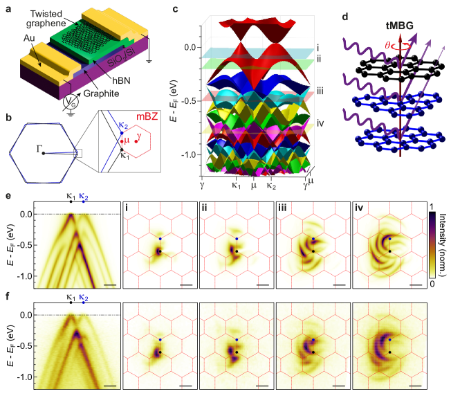
Twisted few layer graphene samples were fabricated on hexagonal boron nitride (hBN) by a modified tear-and-stack approach [39, 40], as described in detail in Supplementary Information (SI) section 1 and Methods. A graphite back gate electrode was incorporated into some of the devices, shown schematically in Fig. 1a. Scanning probe microscopy and scanning photoemission microscopy showed homogeneous regions a few micrometres across in the twisted graphenes. Spatially resolved ARPES spectra were acquired from within these regions at the nanoARPES branch of the I05 beamline at Diamond Light Source, as described in Methods and SI section 2. Energies are measured relative to the Fermi energy, , determined by fitting the drop in photoemission intensity at on a metal electrode connected to the graphene stack.
A hybrid theory-tight-binding model was used to calculate the electronic structure of twisted few layer graphenes, using a full set of Slonczewski-Weiss-McClure (SWMcC) parameters for the aligned multi-layer graphenes [41, 42, 43]. The values of the SWMcC parameters, as given in Table 1 of Methods, were established by earlier transport studies [44] and are used here without fitting to the experimental data. Details of the calculations are given in Methods and SI section 3. We focus on the electronic band structure across the moiré Brillouin zones (mBZs), at the graphene Brillouin zone corners, Fig. 1b. Band-folding results in a rich electronic band structure, as shown in Fig. 1c for twisted monolayer-on-bilayer graphene (tMBG) at a twist angle of .
Not all of these bands are apparent in ARPES spectra and their relative intensities change with measurement conditions. The photoemission intensity depends on matrix elements for the photoexcitation process, resonance and interference effects, and attenuation of the photo-emitted electrons [45]. For complex systems, this can lead to confusion over the interpretation of the ARPES spectra and their relation to electronic band structure calculations, necessitating simulation of the ARPES intensity. To do this, the probability of a photo-stimulated transition from an initial band state in graphene to a hybrid state in vacuum was calculated using Fermi’s Golden Rule [46, 34], as described in Methods and SI section 4. The final state () was assumed to be a plane wave in the vacuum. Travel of the photoelectron to the surface, and escape and detection, were included by accounting for an increased path length for emission from the lower layers, resulting in a phase difference in the plane waves and an attenuation in intensity as shown schematically in Fig. 1d. This phase difference was determined from the out-of-plane component of the final state momentum, ; the validity of this approach was tested by comparison of simulation to measurement for photon energy dependent spectra of bilayer graphene (see SI section 4). Finally, the simulated spectra were convoluted by a Lorentzian peak of width 60 meV to account for experimental broadening [47] due to sample quality, intrinsic linewidth and measurement resolution.
Simulated ARPES spectra for tMBG at , are given in Fig. 1e and compared to the corresponding experimental spectra in Fig. 1f, for which the measured twist angle is . The twist-angle was determined from constant energy maps near , using the replica bands to determine the mBZ and hence . Energy-momentum slices through the corners of the mBZ show the Dirac cones of the primary bands, moiré replica bands, and hybridisation gaps where bands from the rotated monolayer anti-cross with those of the bilayer. Photoemission from bands in the upper monolayer graphene (MLG) is more intense than from those in the bilayer graphene (BLG) underneath, with the replica bands lower in intensity than the corresponding primary bands.
In the ARPES constant energy maps, plotted over the mBZs (shown in red) in Fig. 1e, the primary and replica bands are readily identified near , with the Dirac cones at the mBZ points. However, at deeper energy cuts, interactions between bands make it harder to assign the origin of the photoemission intensity to a specific band in a given layer. The band decomposition at these constant energy slices, determined from the electronic band structure calculations, is shown for comparison in SI section 5. Despite this complexity, it is clear that the model accurately captures both the relative spectral intensities and band positions of the experimental spectra, enabling the electronic structure to be probed in greater detail.
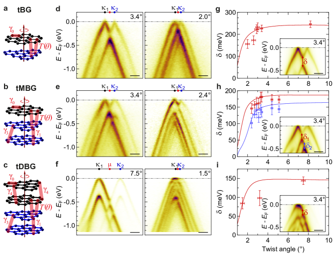
Twist-angle and layer-number dependent spectra. Comparison of spectra acquired from different twist-angles and stacking orders allows a quantitative test of band structure predictions from the ARPES data. In Fig. 2, ARPES energy-momentum slices are presented for twisted bilayer graphene (tBG), twisted monolayer-on-bilayer graphene and twisted double bilayer graphene (tDBG). The twist angle is defined relative to Bernal stacking.
For larger twist angles, , the primary bands are readily resolved in the ARPES spectra with only faint replica bands, whilst at smaller twist angles the intensities of the replica bands increase and the electronic band structure becomes more complex. Quantitative analysis of the replica band intensities near is given in SI section 6 for tBG at different twist angles, showing good agreement between the experimental data and the simulations. In general, the intensity of the replicas decreases in successive mBZs away from the primary bands, as expected due to the lower probability of scattering further in reciprocal space.
Where the bands meet, hybridisation between them results in anti-crossings, with the gaps most obvious at or near the point in the slices shown here. The size of the gaps () at the anti-crossings of the primary bands are plotted in Figs. 2g-i as a function of the twist angle. These were determined by fitting of energy distribution curves (EDCs), as illustrated in the insets of Fig. 2 and described in detail in SI section 7. depends on both the interlayer and intralayer coupling parameters, hence the agreement between experiment (data points) and theory (solid lines) across all twist angles and stacking arrangements demonstrates the accuracy of the theoretical approach for describing the twisted interface. Note that the same SWMcC parameters were used for each structure, without fitting to the experimental data.
At larger twist angles, , the simulations predict that is roughly constant with twist angle, verified by the agreement to the experimental results. In this regime, the anti-crossings occur at energies at which the bands are well described by a linear dispersion and hence scales only with the strength of the potential that couples the states in the different layers. In these simulations, the magnitude of variation of the moiré potential is a constant factor independent of twist angle, related to the interlayer coupling parameters. However, at smaller , the magnitude of the hybridization gap depends sensitively on twist angle and changes subtly with stacking geometry, Figs. 2g-i. At these small twist angles, the anti-crossings lie close to the Dirac points and distort the linear dispersion, as can be seen in the ARPES spectra, forming a band whose bandwidth decreases with twist angle.
Flat band analysis in tDBG. In the smallest twist angle sample measured here, tDBG at 1.5 0.2∘, an almost flat valence band is observed at (Fig. 2f, right-hand panel). A more detailed analysis of this band is shown in Fig. 3. Energy-momentum cuts through the high symmetry points (Figs. 3a-c with their directions indicated on the constant energy plot in Figs. 3d) show ARPES intensity near in all directions, corresponding to the flat band, with a clear gap to the lower lying valence band states.
The band dispersion across the first few mBZs was found from the experimental spectra by fitting EDCs and is shown by the black lines in the right-hand panels of Figs. 3a-c, with the predicted band structure in red. Fig. 3e shows the energy of this valence band edge as a plot; the corresponding plot from the simulations is shown in SI section 8. Although it is at the limit of the experimental resolution here, the flat band has a weak dispersion, periodic across the mBZ as required, with the band minimum at , and is clearly gapped from the lower lying valence bands across all of the mBZ.
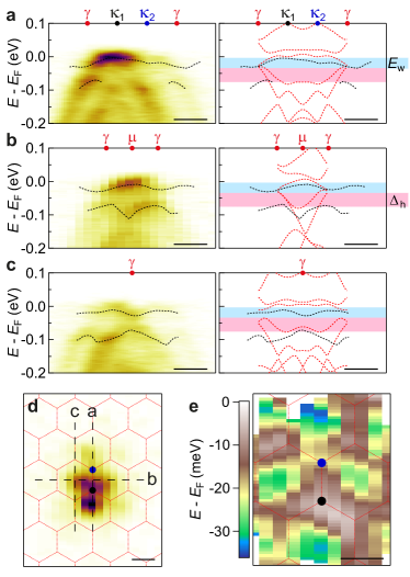
The key band parameters can be determined from this data. The band-width of the flat valence band at is measured to be meV, in good agreement with the predicted value from the electronic structure calculations of meV. The band gap to the next occupied valence band state is smallest at , where it is measured to be meV, significantly greater than the predicted value of meV. Note that the electronic structure calculations here do not incorporate the effects of lattice relaxation which are expected to be significant in determining the low-energy electronic structure in twisted graphenes for small , close to or below the magic-angle [13, 46]. For tDBG at , Haddadi et al. found that the gap at increased by roughly an order of magnitude from meV to meV when lattice relaxation was included [48], consistent with our experimentally determined value. The bandwidth is predicted to decrease further to meV at the magic-angle of , with the gap staying roughly similar in magnitude. A spectrally isolated flatband such as this has been proposed to be favorable for the emergence of correlated insulators [49] and these results prove that, despite previous reports [50, 51], a vertical displacement field is not required to produce such a band in tDBG.
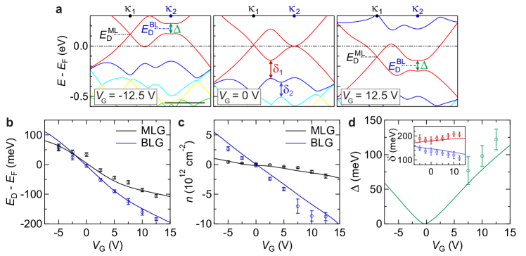
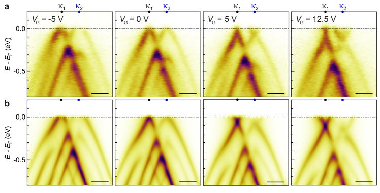
Back-gate-dependent electronic structure. Integrating a back-gate electrode into the tMBG heterostructure, as shown schematically in Fig. 1a, allows the gate dependence of the electronic band structure to be investigated. ARPES spectra at varying for a 3.4 0.1∘ tMBG sample, with hBN dielectric thickness of nm, are shown in Fig. 4a. For positive applied back-gate voltage, , the Dirac point energies move below , corresponding to -doping. There is no apparent broadening of the spectra, indicating a uniform applied field. Consistent with it being the lower layer, closer to the gate electrode, the Dirac point of the BLG, at momentum and energy , shifts more than that of the MLG, at momentum and energy . This indicates partial screening of the back gate [52] and a displacement field across the twisted graphene layers which also opens an energy gap, , at the Dirac point of the BLG [53, 54]. The shift of the BLG bands relative to those of the MLG means that the band anti-crossings occur at slightly different energy and momenta, subtly changing the interactions between bands and hybridisation between layers.
We incorporate the effect of electrostatic gating into the simulations using a self-consistent analysis of on-layer potentials [52]. Starting from the band structure without applied field, potential differences between the layers are added that are proportional to the applied field. The charge redistribution across the layers is determined and the charge density in each layer is used to calculate the screening fields and the resultant modified interlayer potentials. The band structure is recalculated using these modified interlayer potentials and the process iterated to convergence to give a self-consistent response to the applied (see SI section 9 for further details). Simulated ARPES spectra at varying are shown in Fig. 4b, for the same sample geometry as the experimental data (tMBG at with a hBN dielectric thickness of nm, and hBN dielectric constant [55]).
Changes to the band dispersion with are shown in Fig. 5a, emphasising the dominant effects of the applied field: and shift relative to , indicating electrostatic doping in both layers; shifts relative to , consistent with a field transverse to the layers; this field opens a gap, , at the Dirac point of the bilayer graphene [54, 53]. These key parameters were determined by fitting of the spectra. The change in Dirac point energies is plotted in Fig. 5b (solid line from the simulations, data points from the experiment, blue corresponds to BLG and black to MLG). For , , corresponding to electron-doping, while for , corresponding to hole-doping. The resultant charge density, , is plotted in Fig. 5c. For the simulations, is calculated directly from the electronic band structure models by counting the charge in each layer, the experimental data are calculated from and as described in SI section 10.
The charge densities in the bilayer, , and the monolayer, , both scale roughly linearly with , but at a lower rate in the monolayer, , such that most of the charge is localised in the BLG, screening the MLG from the gate. At V there is almost 100 meV difference between and , corresponding to a strong Stark shift due to the displacement field. This changes the BLG dispersion, opening a band gap that scales roughly linearly with the magnitude of and at V is again of order 100 meV. Finally, we note that the shift of the BLG bands relative to those of the MLG results in subtle changes to the interlayer coupling, as can be seen through analysis of the hybridisation gaps. For example, the gaps at the anti-crossings of the primary bands, and as labelled on the band dispersion in Fig. 5a central panel, change in opposite direction with , as shown in the inset of Fig. 5d. For all band parameters, there is good agreement between the experimental measurements and the simulations, confirming the validity of the model used.
We note that our results illustrate a challenge to applying ARPES with in-situ gating to the study of, for example, filling-factor dependent band renormalization in MATBG: a back-gate does not just tune the Fermi level, it also applies a transverse field that subtly changes the hybridisation between layers and hence the Fermi surface. Despite this, ARPES offers a unique capability for resolving the layer-dependent electronic band structure in 2D heterostructures and the evolution of this structure with applied electric field, a crucial control parameter for 2D devices.
Conclusions. Through comparison between measured and simulated ARPES spectra, we have tested the validity of the hybrid theory-tight-binding model for predicting the electronic band structure of twisted few layer graphenes in the small twist angle regime. The simulated spectra quantitatively agree with the measurements, not only from their band dispersions but also their spectral weights, across a range of twist angles () and numbers of layers (tBG, tMBG, tDBG) with a single set of empirically derived parameters describing the inter and intra-layer coupling for twisted and aligned layers. Detailed analysis of the flat band dispersion in twisted double bilayer graphene at , close to the magic angle of [48], shows that although there is close agreement between the hybrid model and the experimental data for the width of the valence band at the Fermi energy, at meV, the gap to the lower lying valence band states is larger than predicted, 46 5 meV, consistent with the importance of lattice relaxation effects at twist angles close to the magic angle. ARPES with in-situ gating reveals the evolution of the electronic band structure with the application of a back gate electrode, demonstrating the importance of both doping and transverse electric field, with quantitative agreement to predicted spectra achieved through a self-consistent approach to modelling the electronic band structure changes with gating. The results reinforce the importance of Stark shifts in 2D heterostructures, even for metallic 2D materials. With this validation, the models can be used with confidence to explore the electronic band structure and emergent transport and optical properties of twisted few-layer graphenes.
Acknowledgements We thank Diamond Light Source for beamtime (proposals SI20573, SI28919 and SI32737).RG acknowledges support from the Royal Society, ERC Consolidator grant QTWIST (101001515) and EPSRC grants EP/V007033/1, EP/S030719/1 and EP/V026496/1. NW acknowledges support from EPSRC grant EP/T027207/1. VF acknowledges support from European Graphene Flagship Core3 Project and EPSRC Grants P/W006502/1 and EP/S030719/1. AM was supported by the EPSRC CDT Graphene-NOWNANO and JN by the University of Warwick and Diamond Light Source.
Methods
Sample fabrication
Samples were fabricated in an argon atmosphere using a modified PMMA-based tear-and-stack technique [39], controlled by a remote micromanipulation rig. Pre-prepared hBN on graphite flakes (on SiO2 substrates) were used as an adhesive layer to tear the graphene flakes supported on a PMMA membrane, allowing accurate control over the twist angle. Samples were annealed in UHV at 300∘C for several hours prior to measurement. For further details see SI section 1.
Angle resolved photoemission spectroscopy
ARPES experiments were performed at the nanoARPES branch of the I05 beamline of Diamond Light Source. A choice of two focusing optics are available to perform spatially resolved ARPES: a Fresnel zone plate for submicrometre spatial resolution, and a capillary mirror for improved flux and energy resolution ( spatial resolution). All photoemission spectra in the main text were measured using the capillary mirror, apart from the tMBG data in the second panel of Fig. 2e which was measured with the zone plate, with a 90 eV photon energy and linearly polarised light, at a sample temperature of K. Experimental constant energy cuts were averaged over 5 meV of the stated energy. For further details see SI section 2.
Tight-binding modelling of electronic structure A hybrid theory-tight-binding Hamiltonian was used for the twisted structures, as previously reported [3, 18, 8]. The SWMcC parameters used for this description are shown in Table 1 and are taken from [44]. Further details are given in SI section 3.
| (eV) | (eV) | (eV) | (eV) | |
|---|---|---|---|---|
| 3.16 | 0.39 | 0.315 | 0.07 | 0.025 |
ARPES simulations. The general form of the ARPES intensity in the central mBZ is written as:
| (1) |
where is the twisted graphene Hamiltonian [56] (see SI section 3).The initial state, , is the wavefunction of the graphene electron, written as a linear combination of Bloch functions at a given point in momentum space, comprised of layer and sublattice components that are coupled using SWMcC parameters as well as mixed by the moiré [57]. The components are solved by diagonalising the respective system Hamiltonian and solving for its wavefunctions. From this, the weights () are computed for each lattice site, where is the layer number and is the sub-lattice index. The final state, , is assumed to be a plane wave in the vacuum. The interaction term adds a small phase shift to the ARPES spectra. Attenuation and interference after photoemission are accounted for by the term: , where per graphene layer was determined by comparison to experiment. Å is the distance between adjacent layers and is the out-of-plane component of the final state momentum, calculated by determining from the conservation of energy () and the kinetic energy of an emitted photoelectron (). The Lorentzian factor broadens the spectra to match the experimental broadening of 60 meV. Further details are given in SI section 4.
References
- [1] Yuan Cao et al. “Unconventional superconductivity in magic-angle graphene superlattices” In Nature 556.7699 Nature Publishing Group, 2018, pp. 43–50 DOI: 10.1038/nature26160
- [2] Yuan Cao et al. “Correlated insulator behaviour at half-filling in magic-angle graphene superlattices” In Nature 556.7699 Nature Publishing Group, 2018, pp. 80–84 DOI: 10.1038/nature26154
- [3] R. Bistritzer and A.. MacDonald “Moire bands in twisted double-layer graphene” In Proceedings of the National Academy of Sciences 108.30 Proc. Natl. Acad. Sci. USA, 2011, pp. 12233–12237 DOI: 10.1073/pnas.1108174108
- [4] Youngjoon Choi et al. “Electronic correlations in twisted bilayer graphene near the magic angle” In Nat. Phys. 15.11 Nature Publishing Group, 2019, pp. 1174–1180 DOI: 10.1038/s41567-019-0606-5
- [5] Lei Wang et al. “Correlated electronic phases in twisted bilayer transition metal dichalcogenides” In Nat. Mater. 19.8 Nature Publishing Group, 2020, pp. 861–866 DOI: 10.1038/s41563-020-0708-6
- [6] Zhiming Zhang et al. “Flat bands in twisted bilayer transition metal dichalcogenides” In Nat. Phys. 16.11 Nature Publishing Group, 2020, pp. 1093–1096 DOI: 10.1038/s41567-020-0958-x
- [7] Shaowen Chen et al. “Electrically tunable correlated and topological states in twisted monolayer–bilayer graphene” In Nat. Phys. 17.3 Nature Publishing Group, 2021, pp. 374–380 DOI: 10.1038/s41567-020-01062-6
- [8] Shuigang Xu et al. “Tunable van Hove singularities and correlated states in twisted monolayer–bilayer graphene” In Nat. Phys. 17.5 Springer ScienceBusiness Media LLC, 2021, pp. 619–626 DOI: 10.1038/s41567-021-01172-9
- [9] Yuan Cao et al. “Tunable correlated states and spin-polarized phases in twisted bilayer–bilayer graphene” In Nature 583.7815 Nature Publishing Group, 2020, pp. 215–220 DOI: 10.1038/s41586-020-2260-6
- [10] Cheng Shen et al. “Correlated states in twisted double bilayer graphene” In Nature Physics 16.5 Nature Publishing Group, 2020, pp. 520–525 DOI: 10.1038/s41567-020-0825-9
- [11] Canxun Zhang et al. “Visualizing delocalized correlated electronic states in twisted double bilayer graphene” In Nat. Commun. 12.1 Nature Publishing Group, 2021, pp. 2516 DOI: 10.1038/s41467-021-22711-1
- [12] Xiaomeng Liu et al. “Spectroscopy of a tunable moiré system with a correlated and topological flat band” In Nat. Commun. 12.1 Nature Publishing Group, 2021, pp. 2732 DOI: 10.1038/s41467-021-23031-0
- [13] Stephen Carr, Shiang Fang and Efthimios Kaxiras “Electronic-structure methods for twisted moiré layers” In Nat. Rev. Mater. 5.10 Springer US, 2020, pp. 748–763 DOI: 10.1038/s41578-020-0214-0
- [14] G. Laissardière, D. Mayou and L. Magaud “Localization of Dirac Electrons in Rotated Graphene Bilayers” In Nano Letters 10.3 American Chemical Society (ACS), 2010, pp. 804–808 DOI: 10.1021/nl902948m
- [15] G. Trambly de Laissardière, D. Mayou and L. Magaud “Numerical studies of confined states in rotated bilayers of graphene” In Phys. Rev. B 86 American Physical Society, 2012, pp. 125413 DOI: 10.1103/PhysRevB.86.125413
- [16] Procolo Lucignano et al. “Crucial role of atomic corrugation on the flat bands and energy gaps of twisted bilayer graphene at the magic angle ” In Phys. Rev. B 99 American Physical Society, 2019, pp. 195419 DOI: 10.1103/PhysRevB.99.195419
- [17] J… Lopes dos Santos, N… Peres and A.. Castro Neto “Graphene Bilayer with a Twist: Electronic Structure” In Phys. Rev. Lett. 99 American Physical Society, 2007, pp. 256802 DOI: 10.1103/PhysRevLett.99.256802
- [18] Aitor Garcia-Ruiz, Hai-Yao Deng, Vladimir V. Enaldiev and Vladimir I. Fal’ko “Full Slonczewski-Weiss-McClure parametrization of few-layer twistronic graphene” In Phys. Rev. B 104.8 American Physical Society (APS), 2021, pp. 085402 DOI: 10.1103/physrevb.104.085402
- [19] Aaron Bostwick et al. “Quasiparticle dynamics in graphene” In Nat. Phys. 3.1, 2007, pp. 36–40 DOI: 10.1038/nphys477
- [20] J M Riley et al. “Negative electronic compressibility and tunable spin splitting in WSe2” In Nat. Nanotechnol. 10.12 Nature Publishing Group, 2015, pp. 1043–1047 DOI: 10.1038/nnano.2015.217
- [21] J. Kim et al. “Observation of tunable band gap and anisotropic Dirac semimetal state in black phosphorus” In Science 349.6249 American Association for the Advancement of Science, 2015, pp. 723–726 DOI: 10.1126/science.aaa6486
- [22] Shujie Tang et al. “Quantum spin Hall state in monolayer 1T’-WTe2” In Nat. Phys. 13.7, 2017, pp. 683–687 DOI: 10.1038/nphys4174
- [23] Neil R. Wilson et al. “Determination of band offsets, hybridization, and exciton binding in 2D semiconductor heterostructures” In Sci. Adv. 3.2, 2017, pp. e1601832 DOI: 10.1126/sciadv.1601832
- [24] Jyoti Katoch et al. “Giant spin-splitting and gap renormalization driven by trions in single-layer WS2/h-BN heterostructures” In Nat. Phys. 14.4, 2018, pp. 355–359 DOI: 10.1038/s41567-017-0033-4
- [25] Wencan Jin et al. “Tuning the electronic structure of monolayer graphene/ Mo S2 van der Waals heterostructures via interlayer twist” In Phys. Rev. B 92.20, 2015, pp. 201409 DOI: 10.1103/PhysRevB.92.201409
- [26] Paul V. Nguyen et al. “Visualizing electrostatic gating effects in two-dimensional heterostructures” In Nature 572.7768 Springer US, 2019, pp. 220–223 DOI: 10.1038/s41586-019-1402-1
- [27] Frédéric Joucken et al. “Visualizing the Effect of an Electrostatic Gate with Angle-Resolved Photoemission Spectroscopy” In Nano Lett. 19.4, 2019, pp. 2682–2687 DOI: 10.1021/acs.nanolett.9b00649
- [28] Ryan Muzzio et al. “Momentum-resolved view of highly tunable many-body effects in a graphene/hBN field-effect device” In Phys. Rev. B 101.20 American Physical Society, 2020, pp. 201409 DOI: 10.1103/PhysRevB.101.201409
- [29] Alfred JH Jones et al. “Observation of electrically tunable van Hove singularities in twisted bilayer graphene from NanoARPES” In Adv. Mater. 32.31 Wiley Online Library, 2020, pp. 2001656 DOI: 10.1002/adma.202001656
- [30] Paul V. Nguyen et al. “Field-Dependent Band Structure Measurements in Two-Dimensional Heterostructures” In Nano Lett. 21.24, 2021, pp. 10532–10537 DOI: 10.1021/acs.nanolett.1c04172
- [31] Viktor Kandyba, Mikhail Yablonskikh and Alexei Barinov “Spectroscopic characterization of charge carrier anisotropic motion in twisted few-layer graphene” In Sci. Rep. 5.1 Nature Publishing Group, 2015, pp. 16388 DOI: 10.1038/srep16388
- [32] I Razado-Colambo et al. “NanoARPES of twisted bilayer graphene on SiC: absence of velocity renormalization for small angles” In Sci. Rep. 6.1 Nature Publishing Group, 2016, pp. 27261 DOI: 10.1038/srep27261
- [33] Han Peng et al. “Substrate doping effect and unusually large angle van Hove singularity evolution in twisted bi-and multilayer graphene” In Adv. Mater. 29.27 Wiley Online Library, 2017, pp. 1606741 DOI: 10.1002/adma.201606741
- [34] J… Thompson et al. “Determination of interatomic coupling between two-dimensional crystals using angle-resolved photoemission spectroscopy” In Nat. Commun. 11.1 Springer ScienceBusiness Media LLC, 2020, pp. 3582 DOI: 10.1038/s41467-020-17412-0
- [35] Takushi Iimori et al. “Electronic structure of 3-twisted bilayer graphene on 4H-SiC (0001)” In Phys. Rev. Mater. 5.5 APS, 2021, pp. L051001 DOI: 10.1103/PhysRevMaterials.5.L051001
- [36] Matthew J Hamer et al. “Moiré superlattice effects and band structure evolution in near-30-degree twisted bilayer graphene” In ACS Nano 16.2 ACS Publications, 2022, pp. 1954–1962 DOI: 10.1021/acsnano.1c06439
- [37] M Utama et al. “Visualization of the flat electronic band in twisted bilayer graphene near the magic angle twist” In Nat. Phys. 17.2 Nature Publishing Group, 2021, pp. 184–188 DOI: 10.1038/s41567-020-0974-x
- [38] Simone Lisi et al. “Observation of flat bands in twisted bilayer graphene” In Nat. Phys. 17.2 Nature Publishing Group, 2021, pp. 189–193 DOI: 10.1038/s41567-020-01041-x
- [39] Riccardo Frisenda et al. “Recent progress in the assembly of nanodevices and van der Waals heterostructures by deterministic placement of 2D materials” In Chem. Soc. Rev. 47.1 Royal Society of Chemistry, 2018, pp. 53–68 DOI: 10.1039/C7CS00556C
- [40] Kyounghwan Kim et al. “Van der Waals heterostructures with high accuracy rotational alignment” In Nano Lett. 16.3 American Chemical Society (ACS), 2016, pp. 1989–1995 DOI: 10.1021/acs.nanolett.5b05263
- [41] J.. Slonczewski and P.. Weiss “Band Structure of Graphite” In Phys. Rev. 109 American Physical Society, 1958, pp. 272–279 DOI: 10.1103/PhysRev.109.272
- [42] J.. McClure “Band Structure of Graphite and de Haas-van Alphen Effect” In Phys. Rev. 108 American Physical Society, 1957, pp. 612–618 DOI: 10.1103/PhysRev.108.612
- [43] J.. McClure “Theory of Diamagnetism of Graphite” In Phys. Rev. 119 American Physical Society, 1960, pp. 606–613 DOI: 10.1103/PhysRev.119.606
- [44] Jun Yin et al. “Dimensional reduction, quantum Hall effect and layer parity in graphite films” In Nat. Phys. 15.5 Springer ScienceBusiness Media LLC, 2019, pp. 437–442 DOI: 10.1038/s41567-019-0427-6
- [45] Andrea Damascelli “Probing the Electronic Structure of Complex Systems by ARPES” In Phys. Scr. T109, 2004, pp. 61–74 DOI: 10.1238/Physica.Topical.109a00061
- [46] Jihang Zhu, Jingtian Shi and Allan H. MacDonald “Theory of angle-resolved photoemission spectroscopy in graphene-based moiré superlattices” In Phys. Rev. B 103 American Physical Society, 2021, pp. 235146 DOI: 10.1103/PhysRevB.103.235146
- [47] M. Mucha-Kruczyński et al. “Characterization of graphene through anisotropy of constant-energy maps in angle-resolved photoemission” In Phys. Rev. B 77.19 American Physical Society (APS), 2008, pp. 195403 DOI: 10.1103/physrevb.77.195403
- [48] Fatemeh Haddadi, QuanSheng Wu, Alex J. Kruchkov and Oleg V. Yazyev “Moiré Flat Bands in Twisted Double Bilayer Graphene” In Nano Lett. 20.4, 2020, pp. 2410–2415 DOI: 10.1021/acs.nanolett.9b05117
- [49] G. Burg et al. “Correlated Insulating States in Twisted Double Bilayer Graphene” In Phys. Rev. Lett. 123.19 American Physical Society, 2019, pp. 197702 DOI: 10.1103/PhysRevLett.123.197702
- [50] Jong Yeon Lee et al. “Theory of correlated insulating behaviour and spin-triplet superconductivity in twisted double bilayer graphene” In Nat. Commun. 10.1 Springer US, 2019, pp. 5333 DOI: 10.1038/s41467-019-12981-1
- [51] Mikito Koshino “Band structure and topological properties of twisted double bilayer graphene” In Phys. Rev. B 99 American Physical Society, 2019, pp. 235406 DOI: 10.1103/PhysRevB.99.235406
- [52] Sergey Slizovskiy et al. “Out-of-Plane Dielectric Susceptibility of Graphene in Twistronic and Bernal Bilayers” In Nano Lett. 21.15 American Chemical Society (ACS), 2021, pp. 6678–6683 DOI: 10.1021/acs.nanolett.1c02211
- [53] Yuanbo Zhang et al. “Direct observation of a widely tunable bandgap in bilayer graphene” In Nature 459.7248 Nature Publishing Group, 2009, pp. 820–823 DOI: 10.1038/nature08105
- [54] Edward McCann “Asymmetry gap in the electronic band structure of bilayer graphene” In Phys. Rev. B 74.16, 2006, pp. 161403 DOI: 10.1103/PhysRevB.74.161403
- [55] Akash Laturia, Maarten L Van de Put and William G Vandenberghe “Dielectric properties of hexagonal boron nitride and transition metal dichalcogenides: from monolayer to bulk” In NPJ 2D Mater. Appl. 2.1 Springer ScienceBusiness Media LLC, 2018, pp. 6 DOI: 10.1038/s41699-018-0050-x
- [56] Eric L. Shirley, L.. Terminello, A. Santoni and F.. Himpsel “Brillouin-zone-selection effects in graphite photoelectron angular distributions” In Phys. Rev. B 51 American Physical Society, 1995, pp. 13614–13622 DOI: 10.1103/PhysRevB.51.13614
- [57] M. Mucha-Kruczynski, J.. Wallbank and V.. Fal’ko “Moiré miniband features in the angle-resolved photoemission spectra of graphene/ heterostructures” In Phys. Rev. B 93 American Physical Society, 2016, pp. 085409 DOI: 10.1103/PhysRevB.93.085409