Wide-field quantitative magnetic imaging of superconducting vortices using perfectly aligned quantum sensors
Abstract
Various techniques have been applied to visualize superconducting vortices, providing clues to their electromagnetic response. Here, we present a wide-field, quantitative imaging of the stray field of the vortices in a superconducting thin film using perfectly aligned diamond quantum sensors. Our analysis, which mitigates the influence of the sensor inhomogeneities, visualizes the magnetic flux of single vortices in YBa2Cu3O7-δ with an accuracy of %. The obtained vortex shape is consistent with the theoretical model, and penetration depth and its temperature dependence agree with previous studies, proving our technique’s accuracy and broad applicability. This wide-field imaging, which in principle works even under extreme conditions, allows the characterization of various superconductors.
Superconducting vortex, as a manifestation of macroscopic quantum effects, is one of the central subjects in the physics of superconductivity. Diverse vortex phases such as vortex lattice, vortex liquid, and Bragg glass appear in type-II superconductors’ mixed state [1, 2, 3]. Those phases and vortex dynamics lead to bulk electromagnetic responses of superconductors and thus have been under vigorous investigation. Besides, since the flux quantization in superconducting vortices originates from the gap symmetry, anomalous quantization such as a half-quantum vortex in –wave superconductors [4, 5] is proposed to emerge as a signature of unconventional pairing symmetry. Therefore, techniques that can quantitatively image quantum vortices under various temperatures, pressures, and magnetic fields would help probe a wide variety of superconductivity with open questions.
Several techniques are available to visualize local magnetic fields [6, 7, 8, 9]. In particular, scanning techniques using sensor chips are widely used for quantitative measurements of magnetic flux density [10, 11, 12, 8]. In such scanning techniques, superconducting quantum interference devices (SQUIDs) [10, 11] and nitrogen-vacancy (NV) centers in diamonds [13, 14] are prominent as sensors. While SQUIDs have excellent sensitivity, NV centers operate under severe environments such as high temperatures and high magnetic fields [15, 16]. Scanning microscopy provides nanoscale spatial resolution and high accuracy [12]. As for the NV-center technique, alternatively, imaging with a wide field of view exceeding is possible with a camera and NV ensemble sensors [17, 9]. This technique is beneficial in terms of high throughput [9]. Furthermore, it can be introduced into extreme environments such as ultrahigh pressure [18, 19, 20], which are not accessible by the scanning technique. Thus, it aids in researching novel superconductors at high temperatures and pressures [21, 22]. Using this technique, efforts have been made particularly to image the stray magnetic fields of superconducting quantum vortices [23, 24], but achieving magnetic accuracy close to the scanning technique [13] has been challenging. The issue arises primarily due to the fact that the measurement of superconductors is conducted in a low magnetic field, where the inhomogeneity of the sensor’s strain parameter [25] and the signal overlap resulting from a diamond sensor ensemble with four NV axes render quantitative analysis to extract field component perpendicular to the superconductors’ surface practically impossible.
Here, we address these issues by utilizing a perfectly aligned NV ensemble sensor [26, 27, 28, 29, 30] and implementing an analysis that eliminates sensor inhomogeneities resulting from strain distribution, complemented by reference measurements in a zero magnetic field. Consequently, we report a quantitative wide-field magnetic imaging of superconducting vortices in a thin film of a typical high- superconductor YBa2Cu3O7-δ (YBCO). The combination of the inherent high throughput of widefield NV microscopy and achieved quantitativeness enables statistical analysis. The obtained statistics is consistent with the single quantization of vortices. Moreover, the stray magnetic field distribution aligns well with theoretical models, offering an alternative method for estimating the magnetic field penetration depth. Our technique, which combines high throughput and accuracy, is helpful for comprehensive characterization, including exploring unconventional superconductors [31, 32, 33].
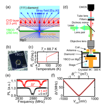
We use NV ensemble sensors at the diamond surface to visualize vortex stray magnetic fields. Figure 1(a) is the measurement schematic. The sensors are located in a thin film grown on a (111) Ib diamond substrate ( mm3) using a chemical vapor deposition (CVD) technique [26, 27, 28, 29, 30]. The symmetry axis of the NV center (NV axis) is perfectly aligned perpendicular to the diamond surface. The CVD-grown NV layer thickness is [Fig. 1(a)], measured by secondary ion mass spectroscopy. The areal density of NV centers and the density of nitrogen atoms are estimated to be and , respectively. We adhere the diamond chip to a YBCO thin film by varnish [Fig. 1(b)]. The stray field from the vortices is detected at the NV centers in the CVD layer at a distance away [Fig. 1(a)]. The YBCO sample is a (100) thin film (S-type) on a MgO substrate purchased from Ceraco Ceramic Coating GmbH. The nominal YBCO thickness is . The critical temperature is estimated to be from the temperature-dependent sheet resistance shown in Fig. 1(c).
Our microscope system is shown in Fig. 1(d). The sample is fixed with vacuum grease to a stage in an optical cryostat (Montana Instruments Cryostation s50). The sample temperature is controlled by a heater and monitored by a thermometer of the stage. Hereafter, we use the stage thermometer value as the temperature. We expand a green laser (532 nm, 120 mW) onto the diamond to image the photoluminescence (PL) of the NV centers. We image the wavelength range of the NV center (– nm) with a CMOS camera and optical filters. The optical diffraction limit is estimated to be nm. Since we acquire the images through the diamond, the optical resolution becomes due to optical aberration [34]. We use a loop microwave antenna [35] fixed on the optical window of the cryostat to manipulate the NV centers. A coil applies a spatially uniform static magnetic field in the direction perpendicular to the YBCO surface, parallel to the NV axis. We perform field-cooling (FC) to generate the vortices by cooling down the stage temperature from to the desired temperature. At the same time, we modulate their density by tuning the field generated by the coil.
Magnetic flux density is obtained using optically detected magnetic resonance (ODMR) in the NV centers [25]. Figure 1(e) shows typical ODMR spectra, where the vertical axis is the relative PL intensity with and without microwave irradiation, and the horizontal axis is microwave frequency. There are two dips in each spectrum, which correspond to electron spin resonances of the NV centers. The splitting between the resonance frequencies is larger at 1 mT (red squares) than at 0 mT (black circles), reflecting the Zeeman effect. The splitting is given by [25],
| (1) |
where is the magnetic flux density in the direction of the NV axis, MHz/mT is the gyromagnetic ratio of an electron spin, and is a strain parameter, which is position-dependent in the crystals. We fit the ODMR spectrum by two Lorentzian to determine and at each position and convert to using Eq. 1 (described later). Note that such a simple analysis is possible thanks to the perfectly aligned NV centers; ordinary ensemble centers have up to eight resonance signals, complicating the investigation. In addition, the absence of the sensors oriented to other symmetric axes is beneficial for the high sensitivity because it prevents contrast reduction [28, 36]. We analyze the data of whole CMOS pixels (1536 pixel 2048 pixel) to obtain the magnetic field distribution. To mitigate the failure of the Lorentzian fitting, we reduce shot noise by smoothing the PL image with a Gaussian filter smaller than the optical resolution (whose decay length is pixels of the camera)(see supplemantal materials for details.)
We calibrate the magnetic field of the system. Figure 1(f) shows the dependence of the splitting on the coil voltage . We obtain this data at a temperature well above to avoid the diamagnetism of superconductivity. increases with increasing the absolute value of the coil voltage, as expected from Ampere’s law. The total magnetic field is obtained as,
| (2) |
where is at the temperature , is the linear coefficient between coil voltage and magnetic field, and is a residual magnetic field, including geomagnetism. The solid black line in Fig. 1(f) is the fitting using Eqs. 1 and 2. It agrees well with our experimental result. We obtain the fitting parameters , and . The calibration accuracy of is (95 % confidence interval).
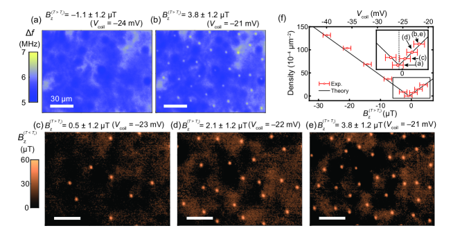
Figures 2(a) and (b) show the distributions of obtained under FC conditions of and , respectively. We obtain these images at 40 K. There are multiple point-shaped magnetic field distributions at the larger field [Fig. 2(b)], while no such distributions at the smaller field [Fig. 2(a)]. Each of these points is a superconducting vortex. Later we prove that they are genuinely single vortices. The absence of such a feature in Fig. 2(a) indicates no vortices in this view, implying minuscule magnetic fields are realized in the cool-down process. We define this condition as zero-field cooling.
Although there is no apparent vortex-like distribution in Fig. 2(a), there is a fluctuating distribution of . The primary cause of this phenomenon is the position-dependent strain in the diamond crystal. We also observe that depends on the excitation light intensity, which can lead to such a distribution [37, 38](see supplemantal materials for details). We find that the latter effect, which is smaller than that of the strain, can be efficiently removed by phenomenologically including it in strain in the following analysis. We calculate the magnetic field density at each pixel using
| (3) |
where is the at zero magnetic fields [Fig. 2(a)]. Figures 2(c), (d), and (e) present the resulting magnetic field distributions obtained under FC of , , and , respectively. Our analysis successfully subtracts the inhomogeneities due to the strain and excitation light intensity, and now vortices are visible more clearly.
We examine the relation between the number of vortices and the magnetic flux density during FC. We count the number of the vortices in the field of view to obtain vortex areal density, as shown in Fig. 2(f). The vortex density increases linearly with the absolute value of the magnetic field. A superconducting vortex has a single flux quantum (where is Planck’s constant and is the elementary charge). The vortex density corresponds to the magnetic flux density. Thus, in Fig. 2(f), the proportionality coefficient should be . The solid black line is the theoretical fitting based on the calibration in Fig. 1(f), consistent with the experimental result within the error bars. As shown by the vertical dashed line in the inset of Fig. 2(f), the zero field calibration is carried out within , corresponding to the exact residual field of , including geomagnetism. These results prove that the observed vortices have a single flux quantum.
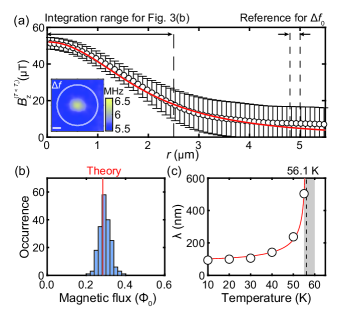
The present method, which observes many vortices in a wide field of view quantitatively and simultaneously, enables us to make a statistical analysis. The inset of Fig. 3(a) depicts the distribution of for a typical vortex. Thus, the magnetic field is isotropically distributed concerning the distance from the vortex center. We rely on Eq. 3 to extract the field, where we define as an average of far away from the vortex center (specifically, ) to avoid the effect of drift during FC cycles. There are 290 vortices in the results obtained under FC of several between and . We estimate the center-of-mass positions of these vortices by Gaussian fitting. Among them, we extract 190 vortices, located away from large inhomogeneity and separated by more than 8 to avoid the effect of drift and the influence of stray fields from neighboring vortices.
Figure 3(a) shows the obtained distribution of the magnetic field of a vortex as a function of . The error bar reflects the standard deviation concerning the 190 vortices used in the analysis. The magnetic field just above the vortex center is , while the error bars are kept as small as .
Figure 3(b) shows the magnetic flux projection obtained by integrating each vortex field over the region of , as indicated by the arrow in the top left of Fig. 3(a). The histogram forms a Gaussian distribution, meaning that all the single vortices are accurately captured as having the same flux. The magnetic flux’s average and standard deviation is and , respectively, showing that the present technique has a precision of 10 %. The statistical uniformity also guarantees that our analysis has successfully removed the observed inhomogeneities. is smaller than because the integration range is limited to and only the field component parallel to the NV axis is detected, as schematically shown in Fig. 1(a).
Next, we quantitatively compare the distribution of the stray field with theory. The stray field from a quantum vortex exhibits different characteristic lengths in bulk [39, 40, 41] and thin-film[40, 41, 42] cases, dictated by the London penetration depth and the Pearl length[43] , respectively. Given that the thickness is nm in our case, comparable to the penetration length (a few hundred nm [44, 45, 46]), we analyze our results using the model derived from Carneiro and Brandt [40], which is applicable to both bulk and thin-film cases(see supplemantal materials for details):
| (4) |
where is 0-th order Bessel function of the first kind, , and is the London penetration depth, which depends on temperature. Our method is subject to the influence of the thickness of the CVD layer and the optical resolution. The solid red line in Fig. 3(a) results from the fitting using a spatially integrated form of Eq. 4 to include these effects, reproducing the experimental result well within the error bars. The calculated flux is also consistent with the statistical results of the magnetic flux shown by the red vertical line in Fig. 3(b). We obtain when we fix . Since we repeat thermal cycles several times and confirm that two-parameter estimation from fitting both and always yields a value of around , we fix hereafter. The vortex size in a superconducting thin film, i.e., the Pearl length, is estimated to be nm, smaller than the optical resolution. The stray field distribution from the vortex appears larger than because the sensor ensemble is located away by from the YBCO film, which disperses the magnetic flux, as shown in Fig. 1(a).
We investigate the temperature dependence of . Figure 3(c) shows the from fitting the experimental result at each temperature obtained by raising temperature after FC of .(see supplemantal materials for full data) The resulting remains at nm from to but dramatically increases above , reaching at . The vortex disappears at between and [a gray area in Fig. 3(c)], lower than the original K, due to the local heating by laser irradiation.
Previous studies report that varies from a minimum of 130 nm to a maximum of 810 nm [44, 45, 46]. The observed behavior of is consistent with them. We fit the temperature dependence of using the following empirical model for a -wave superconductor [47, 48, 49],
| (5) |
We obtain and ; the fitted curve agrees well with the obtained . In some models [43, 50, 51], the covariance of and is large, meaning that might vary depending on (and vise versa), and they might not be well determined by two-parameter fitting. Nevertheless, estimating the scaling behavior of one parameter from the fitting with the other parameter fixed is still meaningful in such a situation. The penetration depth is an essential phenomenological parameter in describing superconductivity, and various methods have studied its behavior. Although the present method is not immune from the effect of laser heating, it provides an important alternative to systematically address this parameter under a wide range of experimental conditions.
To conclude, we have quantitatively established the wide-field imaging of superconducting vortices using a perfectly aligned diamond quantum sensor. By eliminating the effect of inhomogeneity, the magnetic flux of a single vortex in a YBCO thin film was visualized with an accuracy of %. In addition, we demonstrate the quantitative method to examine the penetration depth. We can further improve sensitivity and accuracy by combining techniques such as multi-frequency magnetic resonance [52] and thinner CVD layers [28]. The demonstrated precise high throughput method, applicable over a wide temperature range, helps explore various superconducting properties and statistical evaluation, including their MHz - GHz dynamics [53]. For example, it could apply to investigating an anomalous quantum vortex, such as a half-integer one, and to the high-pressure superconductivity in diamond anvil cells [18, 19, 20].
See the supplemental materials for all the magnetic imaging data in the present experiment, details of the numerics employed for the analysis, descriptions of the fitting methods, and information regarding the sensitivity.
We appreciate K. M. Itoh (Keio University) for providing the cryostat. The authors acknowledge the support of Grant-in-Aid for Scientific Research (Nos. JP22K03524, JP19H00656, JP19H05826, and JP22H04962) and of the MEXT Quantum Leap Flagship Program (Grant No.JPMXS0118067395). Some parts of this work were conducted at (Takeda Clean Room, Univ. Tokyo and Nanofab, Tokyo Tech), supported by Advanced Research Infrastructure for Materials and Nanotechnology in Japan (ARIM), Grant Number JPMXP1222UT1131 and JPMXP1222IT0058. SN is supported by the Forefront Physics and Mathematics Program to Drive Transformation (FoPM), WINGS Program, The University of Tokyo, and JSR fellowship.
References
- Fisher et al. [1991] D. S. Fisher, M. P. A. Fisher, and D. A. Huse, Phys. Rev. B 43, 130 (1991).
- Blatter et al. [1994] G. Blatter, M. V. Feigel’man, V. B. Geshkenbein, A. I. Larkin, and V. M. Vinokur, Rev. Mod. Phys. 66, 1125 (1994).
- Shibata et al. [2002] K. Shibata, T. Nishizaki, T. Sasaki, and N. Kobayashi, Phys. Rev. B 66, 214518 (2002).
- Salomaa and Volovik [1987] M. M. Salomaa and G. E. Volovik, Rev. Mod. Phys. 59, 533 (1987).
- Volovik [1999] G. E. Volovik, J. Exp. Theor. Phys. Lett. 70, 792 (1999).
- Bending [1999] S. J. Bending, Adv. Phys. 48, 449 (1999).
- Celotta et al. [2012] R. J. Celotta, J. Unguris, M. H. Kelley, and D. T. Pierce, Techniques to measure magnetic domain structures, in Characterization of Materials (John Wiley & Sons, Ltd, 2012) pp. 1–15.
- Marchiori et al. [2022] E. Marchiori, L. Ceccarelli, N. Rossi, L. Lorenzelli, C. L. Degen, and M. Poggio, Nat. Rev. Phys. 4, 49 (2022).
- Scholten et al. [2021] S. C. Scholten, A. J. Healey, I. O. Robertson, G. J. Abrahams, D. A. Broadway, and J.-P. Tetienne, J. Appl. Phys. 130, 150902 (2021).
- Kirtley and Wikswo Jr [1999] J. R. Kirtley and J. P. Wikswo Jr, Annu. Rev. Mater. Sci. 29, 117 (1999).
- Finkler et al. [2012] A. Finkler, D. Vasyukov, Y. Segev, L. Ne'eman, E. O. Lachman, M. L. Rappaport, Y. Myasoedov, E. Zeldov, and M. E. Huber, Rev. Sci. Instr. 83, 073702 (2012).
- Kirtley [2010] J. R. Kirtley, Rep. Prog. Phys. 73, 126501 (2010).
- Thiel et al. [2016] L. Thiel, D. Rohner, M. Ganzhorn, P. Appel, E. Neu, B. Müller, R. Kleiner, D. Koelle, and P. Maletinsky, Nat. Nanotechnol. 11, 677 (2016).
- Pelliccione et al. [2016] M. Pelliccione, A. Jenkins, P. Ovartchaiyapong, C. Reetz, E. Emmanouilidou, N. Ni, and A. C. Bleszynski Jayich, Nat. Nanotechnol. 11, 700 (2016).
- Schirhagl et al. [2014] R. Schirhagl, K. Chang, M. Loretz, and C. L. Degen, Annu. Rev. Phys. Chem. 65, 83 (2014).
- Fu et al. [2020] K.-M. C. Fu, G. Z. Iwata, A. Wickenbrock, and D. Budker, AVS Quantum Science 2, 044702 (2020).
- Levine et al. [2019] E. V. Levine, M. J. Turner, P. Kehayias, C. A. Hart, N. Langellier, R. Trubko, D. R. Glenn, R. R. Fu, and R. L. Walsworth, Nanophotonics 8, 1945 (2019).
- Hsieh et al. [2019] S. Hsieh, P. Bhattacharyya, C. Zu, T. Mittiga, T. J. Smart, F. Machado, B. Kobrin, T. O. Höhn, N. Z. Rui, M. Kamrani, S. Chatterjee, S. Choi, M. Zaletel, V. V. Struzhkin, J. E. Moore, V. I. Levitas, R. Jeanloz, and N. Y. Yao, Science 366, 1349 (2019).
- Lesik et al. [2019] M. Lesik, T. Plisson, L. Toraille, J. Renaud, F. Occelli, M. Schmidt, O. Salord, A. Delobbe, T. Debuisschert, L. Rondin, P. Loubeyre, and J.-F. Roch, Science 366, 1359 (2019).
- Toraille et al. [2020] L. Toraille, A. Hilberer, T. Plisson, M. Lesik, M. Chipaux, B. Vindolet, C. Pépin, F. Occelli, M. Schmidt, T. Debuisschert, N. Guignot, J.-P. Itié, P. Loubeyre, and J.-F. Roch, New J. Phys. 22, 103063 (2020).
- Drozdov et al. [2015] A. P. Drozdov, M. I. Eremets, I. A. Troyan, V. Ksenofontov, and S. I. Shylin, Nature 525, 73 (2015).
- Mozaffari et al. [2019] S. Mozaffari, D. Sun, V. S. Minkov, A. P. Drozdov, D. Knyazev, J. B. Betts, M. Einaga, K. Shimizu, M. I. Eremets, L. Balicas, and F. F. Balakirev, Nat. Commn. 10, 2522 (2019).
- Schlussel et al. [2018] Y. Schlussel, T. Lenz, D. Rohner, Y. Bar-Haim, L. Bougas, D. Groswasser, M. Kieschnick, E. Rozenberg, L. Thiel, A. Waxman, J. Meijer, P. Maletinsky, D. Budker, and R. Folman, Phys. Rev. Appl. 10, 034032 (2018).
- Lillie et al. [2020] S. E. Lillie, D. A. Broadway, N. Dontschuk, S. C. Scholten, B. C. Johnson, S. Wolf, S. Rachel, L. C. L. Hollenberg, and J.-P. Tetienne, Nano Letters 20, 1855 (2020).
- Rondin et al. [2014] L. Rondin, J.-P. Tetienne, T. Hingant, J.-F. Roch, P. Maletinsky, and V. Jacques, Rep. Prog. Phys. 77, 056503 (2014).
- Miyazaki et al. [2014] T. Miyazaki, Y. Miyamoto, T. Makino, H. Kato, S. Yamasaki, T. Fukui, Y. Doi, N. Tokuda, M. Hatano, and N. Mizuochi, Appl. Phys. Lett. 105, 261601 (2014).
- Tahara et al. [2015] K. Tahara, H. Ozawa, T. Iwasaki, N. Mizuochi, and M. Hatano, Appl. Phys. Lett. 107, 193110 (2015).
- Ishiwata et al. [2017] H. Ishiwata, M. Nakajima, K. Tahara, H. Ozawa, T. Iwasaki, and M. Hatano, Appl. Phys. Lett. 111, 043103 (2017).
- Ozawa et al. [2017] H. Ozawa, K. Tahara, H. Ishiwata, M. Hatano, and T. Iwasaki, Appl. Phys. Express 10, 045501 (2017).
- Tsuji et al. [2022] T. Tsuji, H. Ishiwata, T. Sekiguchi, T. Iwasaki, and M. Hatano, Diam. Relat. Mater. 123, 108840 (2022).
- Stewart [2017] G. R. Stewart, Adv. Phys. 66, 75 (2017).
- Sarma et al. [2006] S. D. Sarma, C. Nayak, and S. Tewari, Phys. Rev. B 73, 220502 (2006).
- How and Yip [2020] P. T. How and S.-K. Yip, Phys. Rev. Research 2, 043192 (2020).
- [34] S. Nishimura, M. Tsukamoto, K. Sasaki, and K. Kobayashi, In preparation.
- Sasaki et al. [2016] K. Sasaki, Y. Monnai, S. Saijo, R. Fujita, H. Watanabe, J. Ishi-Hayase, K. M. Itoh, and E. Abe, Rev. Sci. Instr. 87, 053904 (2016).
- Tsukamoto et al. [2021] M. Tsukamoto, K. Ogawa, H. Ozawa, T. Iwasaki, M. Hatano, K. Sasaki, and K. Kobayashi, Appl. Phys. Lett. 118, 264002 (2021).
- Fujiwara et al. [2020] M. Fujiwara, A. Dohms, K. Suto, Y. Nishimura, K. Oshimi, Y. Teki, K. Cai, O. Benson, and Y. Shikano, Phys. Rev. Research 2, 043415 (2020).
- Ito et al. [2023] S. Ito, M. Tsukamoto, K. Ogawa, T. Teraji, K. Sasaki, and K. Kobayashi, Journal of the Physical Society of Japan 92, 084701 (2023).
- Clem [1975] J. R. Clem, Journal of Low Temperature Physics 18, 427 (1975).
- Carneiro and Brandt [2000] G. Carneiro and E. H. Brandt, Phys. Rev. B 61, 6370 (2000).
- Kogan [2003] V. G. Kogan, Phys. Rev. B 68, 104511 (2003).
- Kogan et al. [2021] V. G. Kogan, N. Nakagawa, and J. R. Kirtley, Phys. Rev. B 104, 144512 (2021).
- Pearl [1964] J. Pearl, Appl. Phys. Lett. 5, 65 (1964).
- Djordjevic et al. [2002] S. Djordjevic, E. Farber, G. Deutscher, N. Bontemps, O. Durand, and J. Contour, Eur. Phys. J. B 25, 407 (2002).
- Sonier et al. [2007] J. E. Sonier, S. A. Sabok-Sayr, F. D. Callaghan, C. V. Kaiser, V. Pacradouni, J. H. Brewer, S. L. Stubbs, W. N. Hardy, D. A. Bonn, R. Liang, and W. A. Atkinson, Phys. Rev. B 76, 134518 (2007).
- Hassan et al. [2021] A. A. E. Hassan, A. Labrag, A. Taoufik, M. Bghour, H. E. Ouaddi, A. Tirbiyine, B. Lmouden, A. Hafid, and H. E. Hamidi, physica status solidi (b) 258, 2100292 (2021).
- Prohammer and Carbotte [1991] M. Prohammer and J. P. Carbotte, Phys. Rev. B 43, 5370 (1991).
- Basov and Timusk [2005] D. N. Basov and T. Timusk, Rev. Mod. Phys. 77, 721 (2005).
- Stilp et al. [2014] E. Stilp, A. Suter, T. Prokscha, Z. Salman, E. Morenzoni, H. Keller, C. Katzer, F. Schmidl, and M. Döbeli, Phys. Rev. B 89, 020510 (2014).
- Auslaender et al. [2009] O. M. Auslaender, L. Luan, E. W. J. Straver, J. E. Hoffman, N. C. Koshnick, E. Zeldov, D. A. Bonn, R. Liang, W. N. Hardy, and K. A. Moler, Nat. Phys. 5, 35 (2009).
- Acosta et al. [2019] V. M. Acosta, L. S. Bouchard, D. Budker, R. Folman, T. Lenz, P. Maletinsky, D. Rohner, Y. Schlussel, and L. Thiel, J. Supercond. Nov. Magn. 32, 85 (2019).
- Kazi et al. [2021] Z. Kazi, I. M. Shelby, H. Watanabe, K. M. Itoh, V. Shutthanandan, P. A. Wiggins, and K.-M. C. Fu, Phys. Rev. Appl. 15, 054032 (2021).
- Degen et al. [2017] C. L. Degen, F. Reinhard, and P. Cappellaro, Rev. Mod. Phys. 89, 035002 (2017).
Supplemental Information for:
Wide-field quantitative magnetic imaging of superconducting vortices
using perfectly aligned quantum sensors
This Supplemental Material is organized as follows: Section I provides additional information related to the processing of pixel-wise ODMR. Section II describes the evaluation of optical resolution, including the effects of smoothing. Section III shows all the results obtained in this measurement with varying magnetic fields during field cooling (FC). Section IV describes the details of the numerics of the theoretical model and fitting procedures by this model. Section V details the sensor sensitivity.
I Processing of ODMR Spectra
I.1 Strain parameter and optical power intensity
In the main text, we attribute the finite splitting of resonance frequency measured in zero magnetic fields mainly to a local strain distribution. By calibrating relying on Eq. (1) in the main text, we have successfully removed the inhomogeneities.
In the main text, we briefly mention that also depends on the excitation light intensity, which can lead to similar fluctuation. We have found that the distribution of at zero fields depends on the intensity of excitation light, although this effect is much smaller than that of the strain. Figure S1(a) replicates Fig. 2(a) in the main text, which shows the intensity plot of after the zero-field cooling down to . There are no superconducting vortices, which means that average field flux density is extremely low (at least ). However, there exist complex inhomogeneities. Figure S1(b) shows the optical intensity during this measurement without the microwave being applied. The fluctuating patterns in Figs. 1(a) and 1(b) are apparently in a negative correlation.
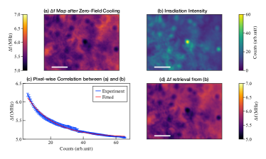
The fact that depends on the optical intensity was reported for the nano-diamond NV center ensemble [1]. We have recently confirmed that a similar phenomenon occurs in a bulk diamond crystal [38]. The present experiment using (111)-oriented bulk diamond also exhibits such a dependence.
We further investigate the optical intensity dependence. Figure S1 (c) shows the correlation between photoluminescence (PL) counts and for each pixel. Here the PL count is rolled into 101 bins, and the scatter plot indicates the mean value of when PL takes a certain value inside the bin. The error bar shows the standard deviation of . shows an exponential decay against the PL intensity. The solid red line is an exponential fit, reproducing well the decaying behavior. Based on this fitting, we can mitigate the effect of due to the optical intensity. Figure S1 (d) shows the distribution calculated from the solid red curve in Fig. S1 (c) and the PL intensity distribution shown in Fig. S1 (b). Figure S1 (d) reproduces Fig. S1 (a) well: the root-mean-squared (RMS) deviation between Figs. 1(a) and (d) is . The splitting in resonance frequency under near zero field is further discussed in [38], where we propose possible mechanisms.
I.2 Pixel-wise ODMR spectrum fitting
In the main text, we perform ODMR measurements in a wide field of view, and we obtain the magnetic flux density by fitting the ODMR spectrum on each pixel of the CMOS camera. The fitting calculations for all pixels of the CMOS censor are executed in parallel using distributed memory multi-process computing implemented in Julia language [3]. It typically takes three minutes to compute using a standard commercial computer.
I.3 Image Smoothing
We apply an image-smoothing technique to improve the signal-to-noise ratio (SNR) [4]. This method interprets the acquired ODMR spectra per pixel as a bundle of images for each applied microwave frequency. Each image of a given frequency is blurred by the optical resolution. Therefore, it is possible to perform image smoothing to the same or less extent as the scale of the optical resolution.
Specifically, we apply Gaussian convolution by a Gaussian kernel whose -width is . The convolution is expressed as follows:
| (S1) |
Here, we denote the PL intensity at the -th pixel as and the kernel function as . We adopt the following Gaussian kernel that takes as the width,
| (S2) |
Equation S1 represents the addition of the counts of surrounding pixels weighted relative to the magnitude of the counts at -th pixel, , set to 1. This sort of convolution increases the total amount of PL counts for each pixel compared to that without the convolution is applied. The PL counts with the convolution is multiplied by a factor of,
| (S3) |
Thus, the SNR of the spectrum improves by about the magnitude of the squared root value .
II Optical resolution
We evaluate the effective optical resolution of our system. Hereafter, we use radii to indicate it.
II.1 Effect of optical aberration
The experimental optical resolution is subject to optical aberration [5, 6]. Specifically, we assume the radius
| (S4) |
for an optical system where the numerical aperture (NA) of the objective lens is , and the measured PL wavelength is . This assumption is based on calculating the point spread function of a single NV center when observed through diamonds with a thickness of around 500 . In addition to optical aberration, the optical resolution is degraded due to image smoothing, described in the following subsection.
II.2 Effect of image smoothing
We evaluate the optical resolution loss due to image smoothing by Gaussian convolution. The actual resolution is given as
| (S5) |
where is the raw optical resolution given in Eq. S4, and is the decay length of the Gaussian kernel. Assuming that the point spread function representing NV centers’ PL intensity distribution can be approximated as a Gaussian function, Eq. S5 is derived as follows. The Gaussian distribution is defined as
| (S6) |
Fourier transformation of this kernel is,
| (S7) |
Therefore, the convolution of two Gaussian functions and with variances of and , respectively, is given by the Fourier transformed form as,
| (S8) |
Thus, we have
| (S9) |
III Full data obtained with varying flux density in Field Cooling
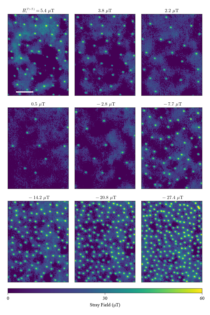
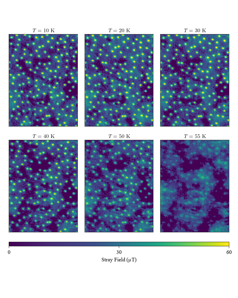
We give all the data used for Fig. 2(f) in the main text here. The results of magnetic field distribution at 40 K for various FC conditions of , are shown in Fig. S3. Furthermore, the results of magnetic field distribution obtained by raising temperature after cooldown in a field of , are shown in Fig. S3.
IV Numerics of the theoretical model and fitting procedures
This section gives the procedure to calculate the theoretical model of vortex stray field distribution [7].
IV.1 Numerics of the theoretical model
The stray field and from a vortex are given as functions of and using the London penetration depth in the cylindrical geometry as [Eq. (8) of Ref. [7]]:
| (S10) | ||||
| (S11) |
Here, the is the first-kind Bessel function of -th order. Also,
| (S12) |
and
| (S13) |
with
| (S14) |
The coefficients are expressed as,
| (S15) |
This model, although not explicitly incorporating the so-called Pearl length , is applicable to both bulk and thin film cases, as stated in [Ref. [7]]. Specifically, in the case of thin films, it can be simplified into the formula [8, 9] that explicitly includes :
| ([Eq. (4)]) | ||||
| ([Eq. (A12,A15) in SI]) | ||||
| ( when ) | ||||
| (Eq. (9) in Ref. [9]) |
In the main text, we calculate Eq. S11, which is expressed in the Fourier-integral form, using adaptive-step numerical integration [10] with a finite cut-off of wavenumber. Next, we calculate the following integral to simulate the experimental result, taking into account the optical resolution and the CVD-grown NV layer thickness ():
| (S16) |
Here, we assume the depth of focus is sufficiently large, which means the kernel of the optical resolution does not depend on the -coordinate. Thus we first execute integral along depth-wise of the NV center layer. Then, we calculate the convolution,
where is the approximated Gaussian kernel corresponding to the optical resolution.
IV.2 Fitting procedures
For the fitting, we minimize the mean squared error (MSE) of the experimental results and the function defined above. This model includes multiple processes of numerical integration and is time-consuming. We thus explore the minimum of MSE by Gradient-less search. In the present result, we start with the 10K data obtained for Fig. 3(c), and we conducted two-parameter fitting as following steps; we first fix and optimize by bounded univariate optimization (Brent’s method [11]). The optimal values for and are then determined by Brute force varying in 0.01 increments. As described in the main text, this model is not highly reliable [12]: it is confirmed that if changing by about 5% () and setting the optimal value of for , the MSE value typically changes by less than only 1%, implying that the best fit might not be so meaningful. However, we also confirmed that changing by 5% with a fixed (or vice versa) increases the MSE by typically about 20%. Thus, fitting with a fixed is still considered to yield more robust information about scaling.
V Sensor Sensitivity
We evaluate the sensitivity of our sensor as follows.
First, we determine the confidence interval of the flux density obtained from fitting the ODMR spectra. An ODMR spectrum consists of Lorentzian forms,
| (S17) |
where corresponds to the resonance frequency, to the resonance linewidth, and to the contrast. The model function of an ODMR spectrum is,
| (S18) |
Here, is the magnetic field, is the strain parameter, and is the zero field splitting. Note that is pre-determined to a fixed value . Consider the case of fitting an experimental ODMR spectrum using this model function. The Jacobian and the residual vector are expressed as,
| (S19) |
The index corresponds to each component of the microwave frequency, and specifies the fitting parameters. We calculate the covariance matrix,
| (S20) |
to obtain the confidence interval, which is defined as the root value of the diagonal components of the covariance matrix Eq. S20, multiplied by Student’s distribution [13].
Next, we evaluate the sensitivity from the obtained confidence interval of the magnetic flux density. We perform fitting using the data with the longest integration time and fix the model function with the parameters obtained at this time. Then, we calculate for each pair of data with varying integration time . The decay rate determines the sensitivity to magnetic flux density in proportion to the square root of the integration time according to shot noise. Precisely, we determine by using the following model,
| (S21) |
Here is determined for each pixel of the camera. Due to the nonlinearity of the model function [Eq. S18] concerning the magnetic field, the sensitivity is also spatially distributed according to the magnetic flux density distribution. Such a distribution is averaged as follows,
| (S22) |
where means pixel-wise average, meaning the inverse of the time to achieve a specific variance on average.
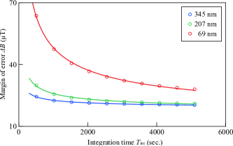
Figure S4 shows the resulting dependence of on the integration time for each size of the convolution range. The legends represent the radii of the Gaussian filter. Both results show squared root decay [Eq. S22]. The respective solid lines represent the fitting. We obtain
| (S23) |
The sensitivity is consistent with the results shown in [14], and is improved by increasing . The gain in SNR by calculating convolution is , as shown in Section I.3. The sensitivity evaluation does not obey a simple linear scaling. The sensitivity has a distribution depending on the magnetic field, and the optimal fitting result should depend on the kernel size . Such an effect is not considered in calculating the margin of error, which possibly explains the absence of linear scaling.
References
- Fujiwara et al. [2020] M. Fujiwara, A. Dohms, K. Suto, Y. Nishimura, K. Oshimi, Y. Teki, K. Cai, O. Benson, and Y. Shikano, Phys. Rev. Research 2, 043415 (2020).
- Ito et al. [2023] S. Ito, M. Tsukamoto, K. Ogawa, T. Teraji, K. Sasaki, and K. Kobayashi, Journal of the Physical Society of Japan 92, 084701 (2023).
- Bezanson et al. [2017] J. Bezanson, A. Edelman, S. Karpinski, and V. B. Shah, SIAM Review 59, 65 (2017).
- Haddad and Akansu [1991] R. Haddad and A. Akansu, IEEE Transactions on Signal Processing 39, 723 (1991).
- Born et al. [1999] M. Born, E. Wolf, A. B. Bhatia, P. C. Clemmow, D. Gabor, A. R. Stokes, A. M. Taylor, P. A. Wayman, and W. L. Wilcock, Principles of Optics: Electromagnetic Theory of Propagation, Interference and Diffraction of Light, 7th ed. (Cambridge University Press, 1999).
- [6] S. Nishimura, M. Tsukamoto, K. Sasaki, and K. Kobayashi, In preparation.
- Carneiro and Brandt [2000] G. Carneiro and E. H. Brandt, Phys. Rev. B 61, 6370 (2000).
- Kogan [2003] V. G. Kogan, Phys. Rev. B 68, 104511 (2003).
- Kogan et al. [2021] V. G. Kogan, N. Nakagawa, and J. R. Kirtley, Phys. Rev. B 104, 144512 (2021).
- Davis and Rabinowitz [2007] P. J. Davis and P. Rabinowitz, Methods of numerical integration (Courier Corporation, 2007).
- Brent [1971] R. Brent, Algorithms for finding zeros and extrema of functions without calculating derivatives, Ph.D. thesis, Stanford University (1971).
- Transtrum et al. [2011] M. K. Transtrum, B. B. Machta, and J. P. Sethna, Phys. Rev. E 83, 036701 (2011).
- Hansen et al. [2013] P. C. Hansen, V. Pereyra, and G. Scherer, Least Squares Data Fitting with Applications (Johns Hopkins University Press, 2013).
- Tsukamoto et al. [2021] M. Tsukamoto, K. Ogawa, H. Ozawa, T. Iwasaki, M. Hatano, K. Sasaki, and K. Kobayashi, Appl. Phys. Lett. 118, 264002 (2021).